1. Introduction
Deep-ultraviolet light (DUV, wavelength < 280 nm) has broad applications in environmental monitoring, food safety, sterilization, non-line-of-sight (NLOS) communication, and analytical science, and has become increasingly important in daily life [
1,
2,
3]. With the implementation of the United Nations’ Minamata Convention on Mercury, mercury-containing ultraviolet sources, represented by mercury lamps, are being phased out worldwide [
4]. This has created an urgent demand for efficient solid-state DUV light sources. Aluminum gallium nitride (AlGaN)-based DUV light-emitting diodes (LEDs), as pollution-free, compact, spectral tunability, and long lifespan solid-state UV sources, have attracted considerable attention, and are expected to gradually replace mercury lamps in the above application scenarios [
5,
6,
7].
Despite significant progress in recent years, the external quantum efficiency (EQE) of AlGaN-based DUV-LED, especially those emitting below 280 nm, generally remains below than 15%, much lower than that of blue and near-ultraviolet LEDs [
8]. The low EQE mainly arises from limited low internal quantum efficiency (IQE) and light extraction efficiency (LEE). For AlGaN epilayers grown on sapphire, the dislocation density can be as high as 10
8 cm
−2, leading to a typical IQE of only about 50% for 275 nm LED devices [
9]. The low LEE is primarily attributed to the increased TM-polarized emission in high-Al-content AlGaN quantum structures [
10], together with severe total internal reflection (TIR) at the sapphire/air or AlGaN/air interface [
11]. Consequently, most of the photons propagate as guided modes within the device and are eventually absorbed or lost in undesired directions. For typical flip-chip DUV LEDs emitting around 275 nm, the critical angle (
θcrit) for TIR is only 33° as calculated from Snell’s law, resulting in an LEE typically below 10% [
12]. Since EQE is determined by the product of IQE, LEE, and injection efficiency, improving LEE is one of the most direct and effective approaches to enhancing the wall-plug efficiency (WPE) of AlGaN-based DUV LEDs.
Extensive efforts have therefore been devoted to improving the LEE of DUV LEDs. Representative strategies include highly reflective electrodes [
13,
14], patterned sapphire substrates (PSS) [
15,
16], and plasmonic scattering nanoparticles [
17,
18], which increase the probability of light extraction from the p-type of flip-chip LEDs. Other approaches, such as micro/nanostructured LEDs [
19], tilted or rough sidewalls [
20,
21], and plasmonic wave-vector-converting structures [
22], have been to developed to redirect TM mode photons and promote their escape. To mitigate TIR loss, refractive-index matching or gradient refractive-index structure have also been explored, including roughened output surfaces [
23], gradient-index encapsulation layers [
24], and micro/nanoscale scattering particles. More recently, metasurfaces composed of subwavelength optical elements have emerged as a versatile platform for controlling photon propagation and enhancing LED light extraction [
25]. By engineering phase gradients and effective refractive-index profiles, metasurfaces can couple guided modes into radiative modes, enabling enhanced and directional emission. Substantial emission enhancement and beam steering have been demonstrated in visible LEDs using disordered silver nanoparticles [
17], structured nanoribbons [
26], symmetry-breaking silicon nanorods [
27], hybrid metallic-Bragg cavity [
28], etc. However, these approaches often require complex nanofabrication or are mainly limited to visible wavelengths. Scalable metasurface designs that are nanofabrication compatible with DUV materials and mass production remain insufficiently explored.
In this study, we propose and demonstrate a dielectric metasurface with surface light outcoupling functionality to enhance the LEE of the flip-chip DUV LEDs, by introducing a novel photon wave-vector modulation mechanism for improving light extraction. The metasurface, consisting of pyramid-shaped nanostructures or void arrays formed in the dielectric layer, was fabricated on the top side of the sapphire substrate via nanoimprinting methods. Theoretical analysis reveals that the nanostructured dielectric interface can break the in-plane translational symmetry of the planar emission surface and provide additional momentum components for photon outcoupling. For the subwavelength pyramid-shaped metasurface, local optical-field modulation and wave-vector redistribution facilitate the coupling of high-angle photons into radiative channels, while for structures with larger feature sizes, geometrical redirection, diffraction, and surface scattering play more dominant roles. As a result, the light output power (LOP) of DUV LEDs emitting near 275 nm is increased by more than 8%. Owing to its process simplicity, scalability, and compatibility with wafer-level fabrication, the proposed dielectric metasurface provides a promising route for improving light extraction in DUV LEDs and other light-emitting devices.
3. Results and Discussion
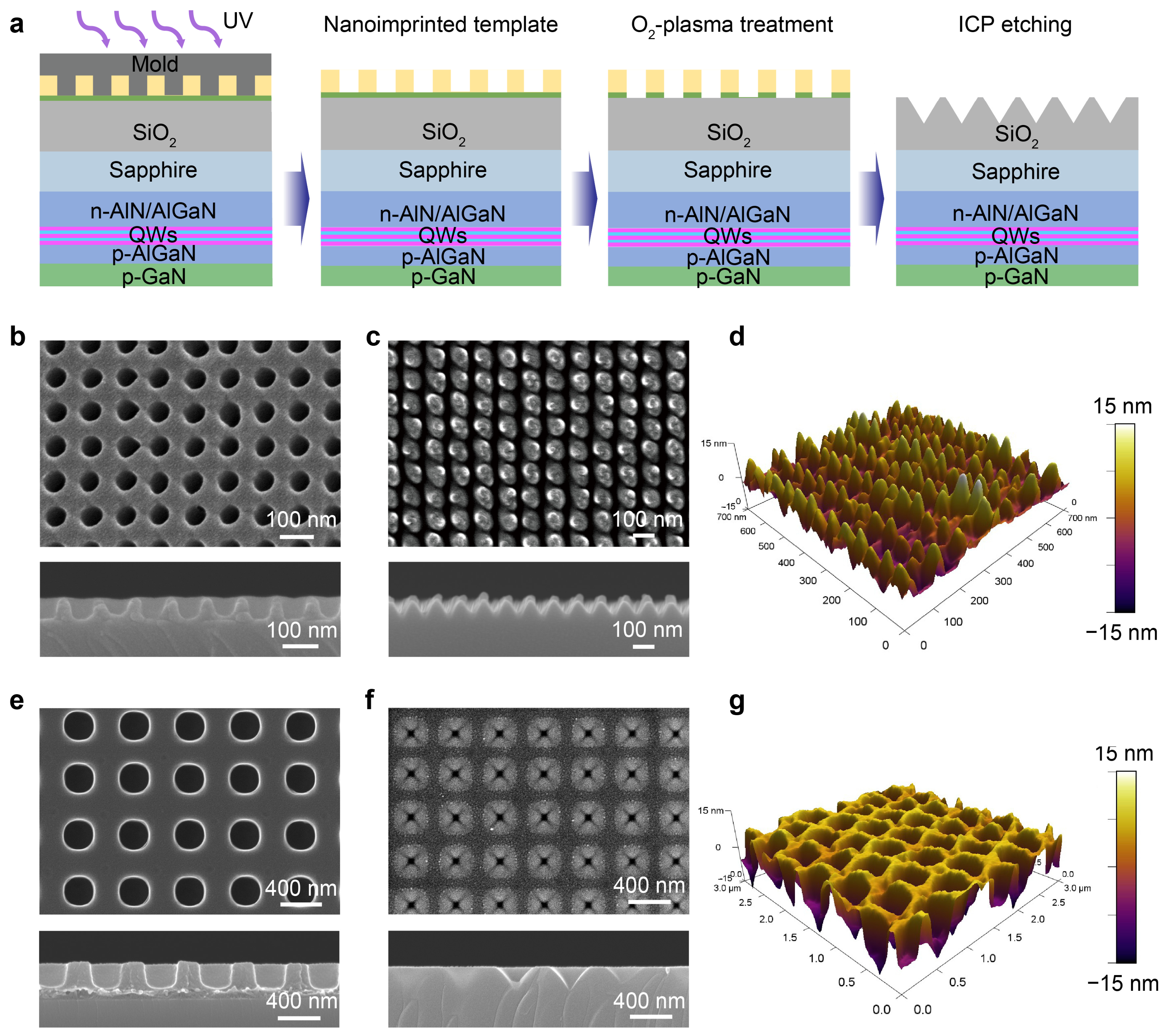
In this work, we designed a dielectric metasurface structure that can be integrated on the light-emitting side of a sapphire substrate of AlGaN DUV LEDs for improving the device’s critical angle of emission, thereby improving the overall LEE. The dielectric matasurface was fabricated using the nanoimprinting method combined with ICP etching, as illustrated in
Figure 1a. A 500 nm thick SiO
2 layer was deposited on the sapphire substrate as the dielectric layer with the function of gradual change in refractive index from sapphire to air. Then, the nanocolumn template structure was transferred onto the deposited double-layer imprinting adhesive using UV nanoimprinting and used as the initial template structure for subsequent nanostructure preparation. ICP etching was subsequently adopted to obtain the final pyramid-shaped nanostructures or voids, due to the thinner imprint mask layer and a certain degree of isotropic etching effect.
Here, two kinds of nanoimprinting templates with different periods, namely the 100 nm period (hole diameter is 50 nm and depth of 50 nm) and the 450 nm period (hole diameter is 250 nm and depth of 200 nm) were used to fabricate the dielectric metasurface.
Figure 1b–g shows the SEM and AFM images of the template and nanoarray and the corresponding cross-section before and after etching, respectively. The results show that the fabricated SiO
2 pyramid structure has a diameter of 90 nm and depth of 60 nm for the 100 nm periodic template after etching, and a diameter of 250 nm and depth of 200 nm for the 450 nm period template.
The light modulation effect of this dielectric nanostructure-based metasurface was first analyzed using classical optical theory, as shown in
Figure 2a. Theoretically, for a planar sapphire/air interface, photons propagating inside the sapphire substrate can escape into air only when their incident angle is smaller than the critical angle (
θcrit), determined by Snell’s law:
where
n1 and
n2 are the refractive indices of the incident and transmitted media, respectively, with
n1 >
n2. At a wavelength of ~275 nm, the refractive indices of the sapphire substrate, SiO
2, and air are 1.82, 1.49, and 1.00, respectively. Therefore, the critical angle for the sapphire/air interface is approximately 33°, while that for the SiO
2/air interface is approximately 42°. For a planar sapphire/SiO
2/air multilayer, however, the insertion of a SiO
2 layer does not intrinsically enlarge the escape-cone angle (
θ1) inside the sapphire substrate. In a planar multilayer system, the in-plane wave vector (
k||) is conserved across the parallel interfaces, which can be expressed in ray optics as the conservation of
n·sin
θ. Equivalently, the in-plane wave-vector component is given by:
where
k0 = 2π/
λ is the wave-vector in free space, and
n is the refractive index of the final light-emitting material. For a flat output interface, photons can be coupled into propagating modes in air only when |
k||| ≤
k0. Otherwise, photons with |
k||| >
k0 cannot satisfy the radiation condition in air and are therefore confined or reflected into the high-index medium. In this sense, the light extraction enhancement cannot be simply attributed to an increased critical angle induced by the SiO
2 layer.
However, the SiO
2 pyramid-shaped nanostructures or void arrays could modify the photon outcoupling process by breaking the translational symmetry of the planar interface. The nanostructured surface provides additional channels for momentum modulation, enabling trapped photons to be scattered, diffracted, or redirected into radiative modes [
29]. For a periodic or quasi-periodic nanostructured interface, this momentum-assisted outcoupling can be qualitatively described as [
30]:
where
G = 2π/
p is the reciprocal-lattice vector associated with the structural period
p, and
m is an integer diffraction or scattering order. Depending on the sign of
m and the direction of
G, the metasurface can either increase or decrease the magnitude of the in-plane wave-vector. When the modified in-plane wave vector satisfies |
k||,out| ≤
k0, photons that would otherwise be trapped can be coupled into radiative modes in air. Therefore, the enhanced light extraction could be interpreted as a result of photon momentum redistribution and propagation-direction modulation. Obviously, unlike conventional surface roughening, which primarily enhances light extraction by introducing random scattering centers to redirect trapped photons, the periodic nanoscale dielectric metasurface provides a deterministic photonic momentum modulation pathway.
For the 100 nm period pyramid array, the feature size is below the DUV wavelength. Such a subwavelength nanostructure can induce local optical-field modulation near the SiO
2/air interface and perturb evanescent or guided optical modes. Although high-order propagating diffraction modes are not expected in air for a strictly periodic 100 nm array at 275 nm, the nanoscale pyramidal morphology can still introduce localized momentum components through near-field scattering at the sharp tips, inclined sidewalls, and spatially varying dielectric boundaries. These effects facilitate the coupling of trapped or high-angle photons into radiative modes. As illustrated in
Figure 2b, the effective outcoupling angular range (
θ2) is thereby broadened. In addition, the densely packed subwavelength nanostructure may also contribute to reduced effective Fresnel reflection at the SiO
2/air interface, owing to the gradual refractive-index transition associated with the pyramidal profile.
For the 450 nm period array, the feature size is comparable to or larger than the emission wavelength, and geometrical redirection and diffractive scattering become more significant. The inclined pyramid facets provide tilted output interfaces that reduce the local incident angle and redirect photon trajectories. Meanwhile, the periodicity of the array can provide additional in-plane momentum for coupling guided photons into free-space radiation, and the roughened surface formed during prolonged ICP etching further enhances light extraction through random scattering. These mechanisms collectively increase the probability that photons trapped by TIR are coupled into the escape cone, leading to enhanced LEE, and enlarged escape angle (
θ3), as illustrated in
Figure 2c.
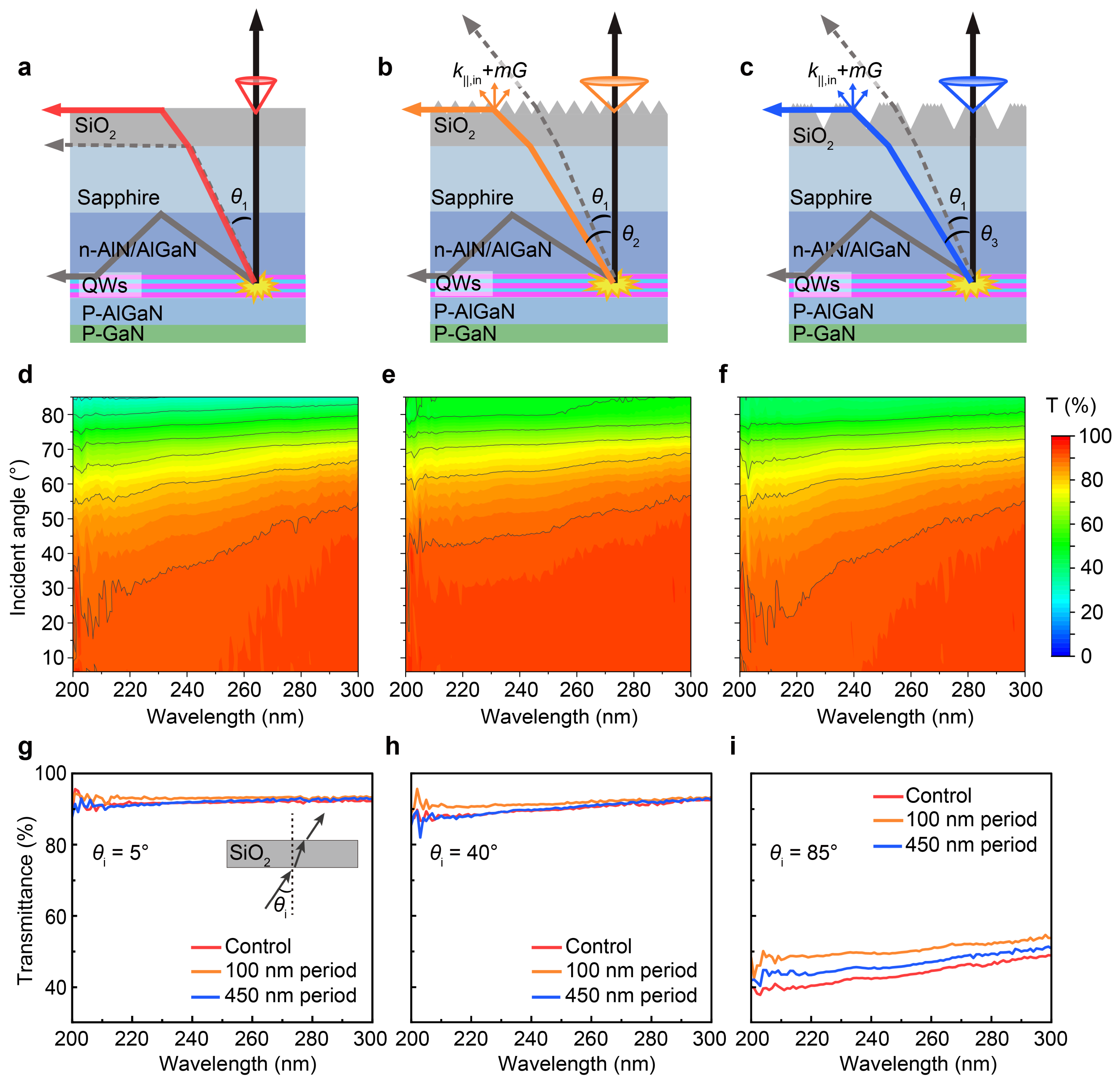
Understandably, with the aid of the dielectric metasurface integrated on the emission side of DUV LED, more photons can be outcoupled smoothly into the air through the additional provided momentum component and local wave-vector redistribution provided by the nanostructured dielectric interface. To experimentally verify the enhanced photon outcoupling induced by the dielectric metasurface, the angle-dependent transmittance (
T) of two nanostructured samples fabricated on quartz substrates was measured and compared with that of a bare quartz substrate (
Figure 2d–f). During the measurement, incident light entered from the flat side of the substrate, propagated through the substrate, and exited from the side containing the nanostructures. The incident angle (
θi) is defined as relative to the surface normal, as illustrated in the inset of
Figure 2g. Therefore, a large incident angle corresponds to a high in-plane wave-vector component inside the substrate, which is analogous to the near TIR condition for photons escaping from the substrate to air.
The results show that at small incident angles, all three samples exhibit extremely high transmittance in the DUV band (200 nm to 300 nm), reaching over 90%. This result can also be seen in the transmission spectrum curve at 5°, as extracted and shown in
Figure 2g. As the incident angle increases (
Figure 2h,i), the transmittance of the bare quartz substrate decreases significantly because of increasing Fresnel reflection and the reduced outcoupling probability near the escape-cone boundary. In contrast, the nanostructured metasurface samples maintain higher transmittance at large incident angles. For example, under 85° incidence at 275 nm, the transmittance of the bare quartz substrate decreases to approximately 30%, whereas the 100 nm period and 450 nm period metasurface samples still exhibit transmittances of 52.2% and 49.2%, respectively.
Obviously, the enhanced broadband transmission near the TIR condition confirms that the dielectric metasurface promotes photon outcoupling by modifying the momentum-matching condition at the output interface. For a flat substrate/air interface, the in-plane wave vector is conserved, and photons with an in-plane wave-vector component exceeding that allowed in air are reflected back into the substrate. In contrast, the pyramid-shaped dielectric metasurface breaks the in-plane translational symmetry and provides additional spatial momentum components. As a result, part of the high-angle photons can be scattered, diffracted, or redirected so that their in-plane wave-vector components are reduced or compensated to satisfy the radiation condition in air. This process increases the photon escape probability, especially when the incident angle approaches the critical angle.
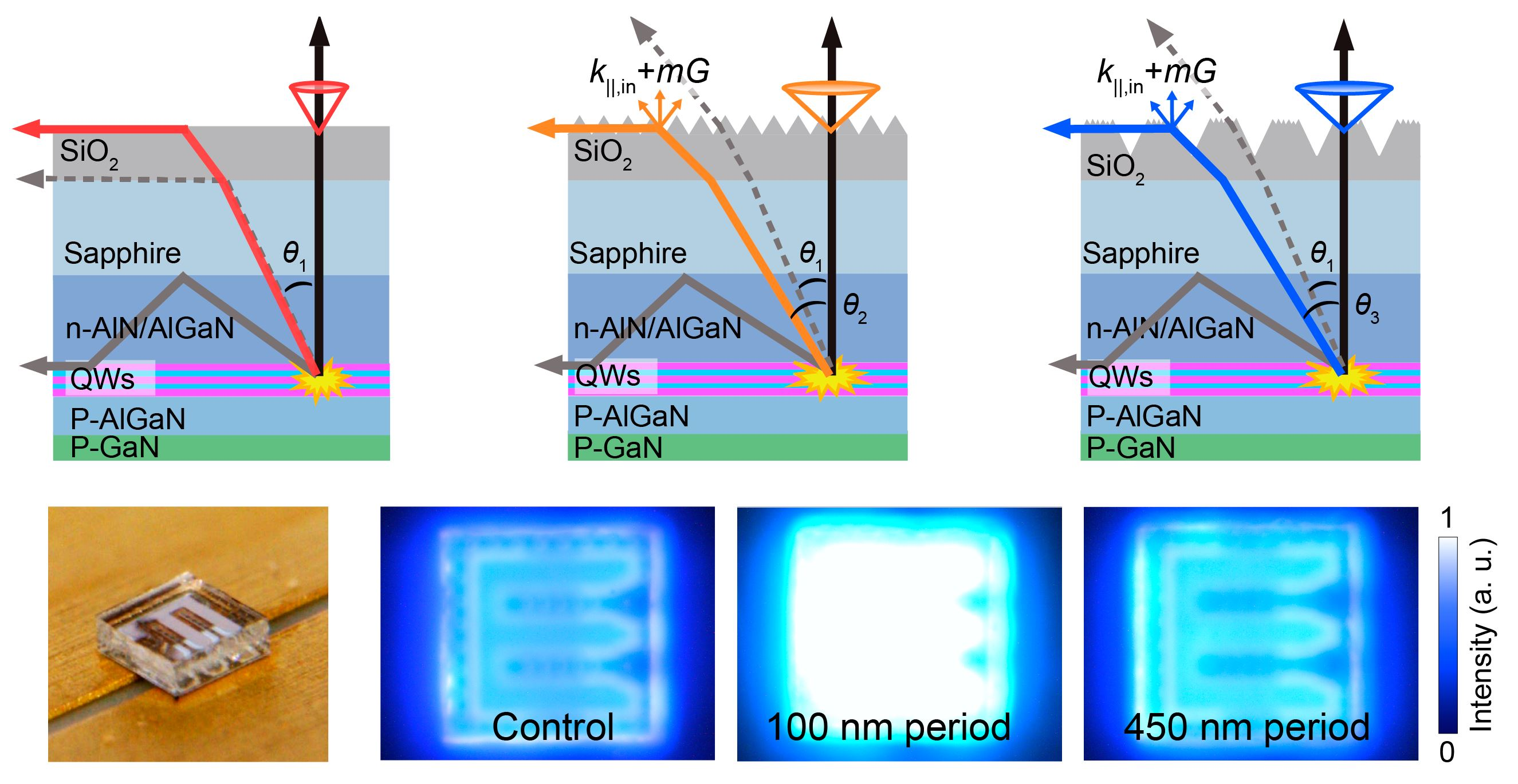
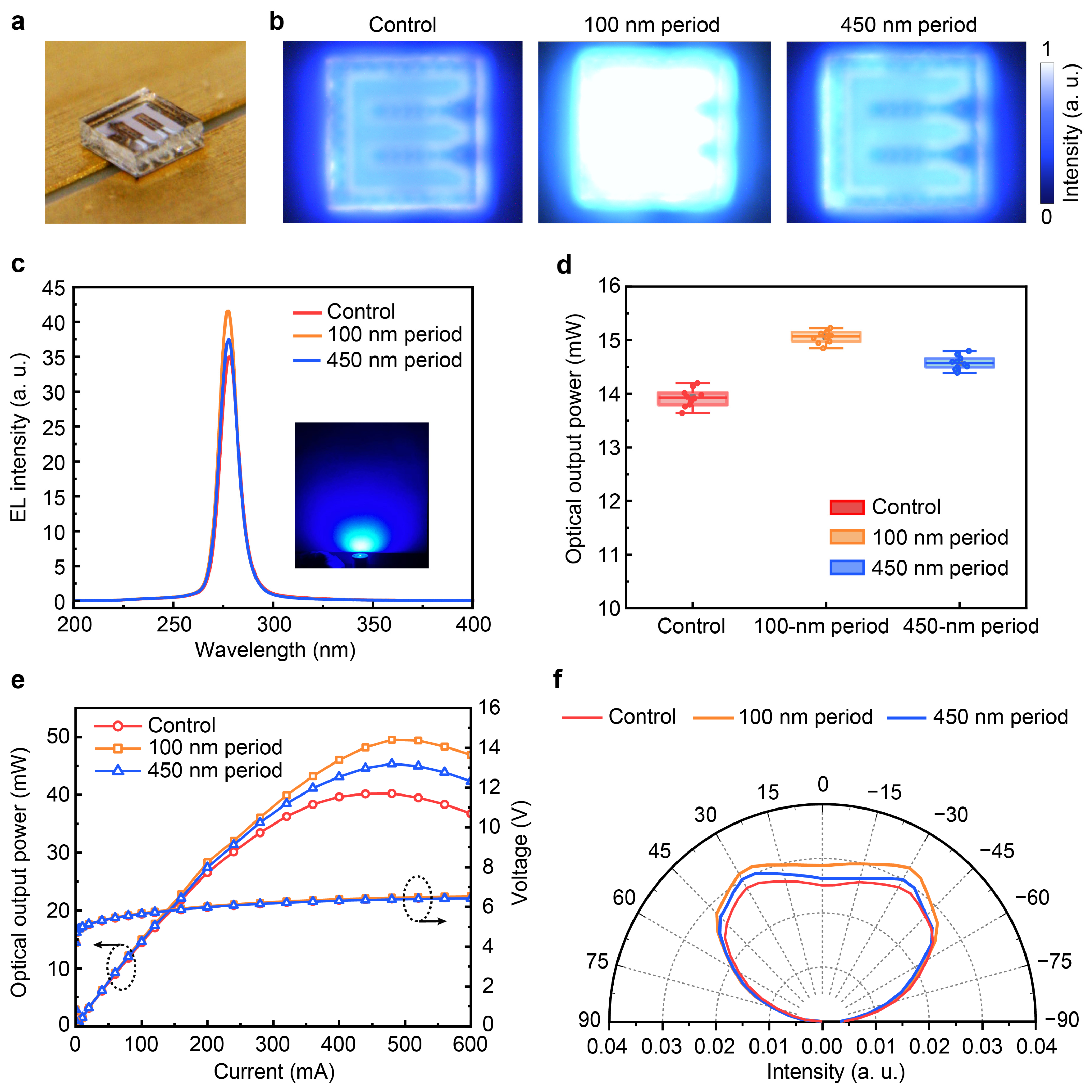
To verify the improved light outcoupling enhancement by the dielectric metasurface, flip-chip AlGaN-based DUV LEDs integrated with the metasurface were fabricated and evaluated by the optoelectronic measurement. A photograph of a representative fabricated flip-chip DUV LED is shown in
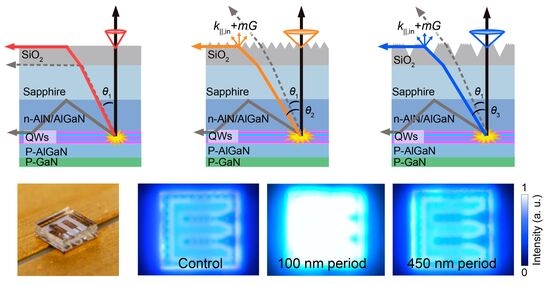
Figure 3a. Driven by a constant current of 100 mA, the near-field emission pattern of the control device and the devices integrated with dielectric metasurface are shown in
Figure 3b. Compared with the control device, the LED integrated with the 100 nm period metasurface achieved a significant improvement in emission intensity, followed by the device with the 450 nm period metasurface, indicating improved photon extraction from the device. The corresponding electroluminescence (EL) spectra are displayed in
Figure 3c. All samples show a similar emission peak located at approximately 277 nm, with no obvious peak wavelength shift after metasurface integration. This indicates that the dielectric metasurface mainly modifies the photon outcoupling process rather than altering the active-region emission characteristics. A representative DUV LED integrated with dielectric metasurface operated at an injection current of 100 mA is shown in the inset of
Figure 3c. A piece of white paper was placed in front of the light-emitting facet to convert the DUV emission into visible blue light, thereby visualizing the device emission. The statistical optical output power of a batch of devices is summarized in
Figure 3d. At an injection current of 100 mA, the corresponding mean ± standard deviation (S. D.) values were 13.92 ± 0.17 mW, 15.06 ± 0.12 mW, and 14.58 ± 0.13 mW for the control, 100 nm period, and 450 nm period devices, respectively. Compared with the control device, the LEDs integrated with the 100 nm periodic dielectric metasurface show an average optical output power enhancement of 8.19%, while those with the 450 nm periodic metasurface exhibited an average enhancement of 4.74%. The larger improvement obtained from the 100 nm period metasurface suggests that the subwavelength dielectric nanostructure is more effective in promoting photon extraction, likely due to its stronger local wave-vector modulation and enhanced outcoupling. The results are consistent with the above classical analysis and angle-dependent transmittance measurements.
The corresponding current-dependent voltage and optical output power characteristics of representative devices are shown in
Figure 3e. The voltage characteristics of the three types of devices are nearly identical, indicating that the integration of the dielectric metasurface does not degrade the electrical injection properties of the DUV LEDs. In contrast, the optical output power follows the same enhancement trend observed above, with the 100 nm period metasurface device showing the highest output power. All devices reach their maximum optical output power at drive currents of approximately 400–500 mA.
Figure 3f compares the far-field radiation patterns of the three type LEDs. Compared with the control device, the DUV LED integrated with dielectric metasurfaces exhibit a pronounced enhancement in far-field intensity over a wide angular range from 0° to ±60°. This broadened and intensified angular emission confirms that the metasurface facilitates the extraction of photons over a wide range of propagation directions, thereby contributing to the overall improvement in optical output power.
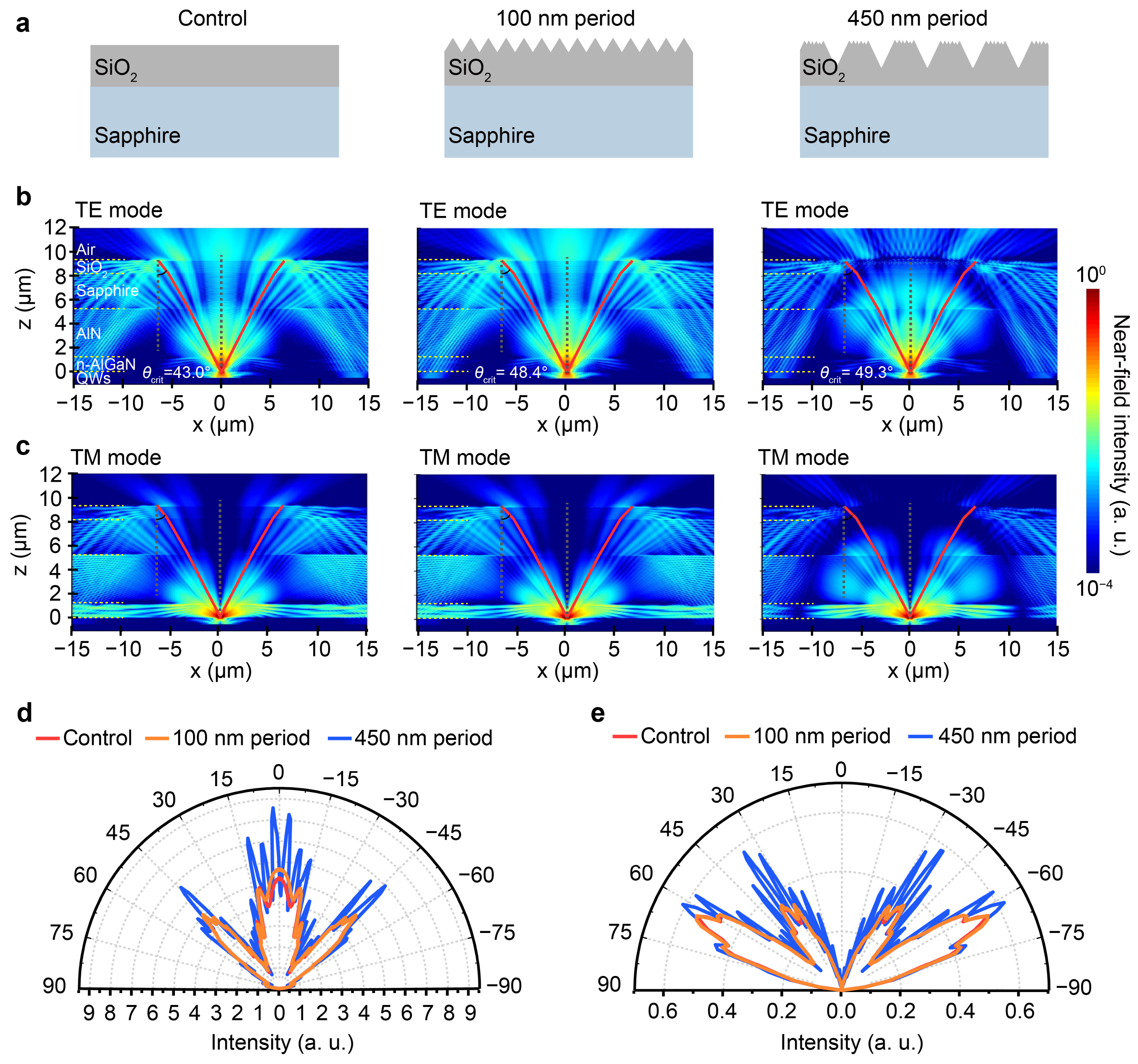
To further reveal the microscopic mechanism of light extraction enhancement in DUV LEDs enabled by dielectric metasurfaces, three-dimensional finite-difference time-domain (FDTD) simulations were performed to analyze the transmission and extraction behaviors of point dipole sources in the device structures. The configurations of the light-emitting surfaces are illustrated in
Figure 4a. Typical cross-sectional near-field distributions under transverse-electric (TE) and transverse-magnetic (TM) dipole excitations were extracted for the three structures, as shown in
Figure 4b,c. The angular propagation characteristics of the locally extracted optical fields were also estimated from the near-field intensity contours to visualize the effective photon outcoupling range.
For the control sample, the extracted optical field is mainly confined within a relatively narrow emission cone, with an estimated critical escape angle (θcrit) of approximately 43.0°, which is close to the critical angle of approximately 42° expected for the SiO2/air interface. This indicates that photon extraction from the planar emission interface is primarily limited by TIR and in-plane wave-vector conservation. After introducing the 100 nm period dielectric metasurface, the near-field distribution shows a broader effective outcoupling range, with the extracted emission extending to approximately 48.4°. Obviously, the subwavelength pyramid array perturbs the local optical field and breaks the in-plane translational symmetry of the planar interface, thereby introducing additional momentum components and enabling local wave-vector redistribution. As a result, part of the photons with large in-plane wave vectors can be coupled into radiative channels, thus broadening the emission angle.
For the 450 nm period structure, the near-field distribution also exhibits an expanded effective outcoupling range, with the extracted optical field extending to approximately 49.3°. In this case, the enhancement is mainly associated with geometrical redirection, diffraction, and scattering induced by the larger pyramid-shaped voids. The inclined facets modify the local photon propagation direction, while the larger periodicity causes more pronounced interference and angle-dependent modulation, resulting in less uniform extraction behavior, as shown in the extracted near-field distribution.
These observations are generally consistent with the calculated LEE of the point dipole sources. The extracted LEEs for the control, 100 nm period, and 450 nm period structures are 1.15%, 1.19%, and 1.16%, respectively. The 100 nm period metasurface shows the most pronounced enhancement, confirming the effectiveness of subwavelength optical-field modulation and momentum-assisted outcoupling. It should be noted that the absolute LEE values and enhancement ratios obtained from the simulations may not quantitatively reproduce the experimental results, because a simplified and laterally scaled-down FDTD model was used to computational cost. In particular, the finite simulation domain cannot fully include photons undergoing long-range lateral propagation, multiple internal reflections, or waveguiding in the actual large-area device before being extracted by the metasurface, which may lead to an underestimation of the light extraction enhancement. Nevertheless, the simulations capture the essential optical modulation mechanism and reproduce the observed enhancement trend.
The near-field distributions under TM dipole excitation are shown in
Figure 4c. The effective outcoupling ranges and extraction trends are generally consistent with those under TE excitation. However, TM-polarized photons are more likely to couple into laterally propagating guided modes within the quantum-well and waveguide layers, which limits their direct front-side extraction. The dielectric metasurface can partially perturb and redirect these guided or high-angle photons, but the enhancement remains constrained by the intrinsic propagation behavior of TM emission in high-Al-content AlGaN-based DUV LEDs.
The far-field emission patterns of the two-dimensionally arranged metasurface arrays were further analyzed, as shown in
Figure 4d,e. Under TE excitation, both the 100 nm period and 450 nm period metasurfaces exhibit enhanced emission compared with the control sample. The 100 nm period metasurface provides relatively smoother and more uniform enhancement, while the 450 nm period structure shows stronger angle-dependent intensity modulation due to geometrical redirection, diffraction, and interference effects. The strong interference feature mainly originates from the idealized and strictly periodic structure used in the simulation model, which can give rise to coherent diffraction/interference effects in the calculated far-field distribution. Under TM excitation, similar far-field characteristics are observed, although the enhancement in the forward direction is less pronounced due to the lateral propagation tendency of TM-polarized photons. These simulation results are consistent with the theoretical analysis and transmission measurements, confirming that the dielectric metasurfaces improve light extraction through momentum redistribution, near-field scattering, and photon trajectory redirection. The results are also consistent with the experimental far-field radiation patterns shown in
Figure 3f, where a more spatially averaged and uniform enhancement of light extraction is observed. This can be attributed to the large-area emission region of the actual device, which averages out the coherent diffraction/interference effects associated with the nanoscale metasurface structures.



 ,
,