1. Introduction
Inertial confinement fusion (ICF) represents a cutting-edge field in modern physical sciences. In ICF, high-energy lasers or secondary X-ray radiation interact with microtargets to trigger deuterium–tritium plasma fusion under extreme condition pellets. This process emits significant radiation across multiple spectral bands. Optical systems are used to image the high-temperature and high-density plasma in the implosion region, acquiring dynamic images and other crucial data. Key physical phenomena in this process occur on micrometer spatial scales and nanosecond time scales. This presents a dual challenge for diagnostics: attaining sub-micrometer spatial resolution and picosecond temporal precision [
1,
2,
3].
Common ultrafast diagnostic tools in ICF and related research include framing cameras, streak cameras, compressive sensing ultrafast imaging systems, and so on [
4]. Framing cameras enable high spatiotemporal resolution two-dimensional imaging and could be categorized into four types, which are respectively based on microchannel plate (MCP) [
5], electron pulse dilation [
6], all-solid-state [
7], and all-optical solid-state [
8]. As core diagnostic instruments in ICF research, framing cameras have seen remarkable technological progress. Early MCP-based framing systems achieved a temporal resolution of 60–100 ps, while electron pulse dilation techniques improved this to 4 ps [
9]. Although these systems meet temporal resolution requirements, evolving ICF demands highlight the need to address their bulkiness and dependence on high voltage. To capture multiple frames, such systems are often integrated with pinhole arrays or Kirkpatrick–Baez (KB) microscopes. These generate multiple images on distinct regions of the MCP microstrip cathode [
10,
11]. However, geometric distortions caused by multi-field-of-view imaging hinder precise single-line-of-sight (SLOS) reconstruction [
12]. With advancements in semiconductor, CMOS-based all-solid-state framing technology has demonstrated notable advantages. Its integrated design overcomes the size limitations of traditional systems and achieves breakthroughs in SLOS imaging [
13,
14].
In 2008, Berger et al. engineered a compact CMOS image sensor test chip for high-speed imaging [
15]. This chip featured a 64 × 64 pixel array and adjustable exposure times ranging from 75 to 305 ps. Building on this design, a team at the Lawrence Livermore National Laboratory (LLNL) introduced a 512 × 512 pixel array readout integrated circuit (ROIC) in 2012. This design incorporated an extended H-tree architecture to enable four-frame imaging [
16]. In 2015, Futa Mochizuki’s group at Shizuoka University developed a 32-segment CMOS image sensor capable of continuous imaging at 200 million frames per second [
17]. The ultrafast diagnostics team at Shenzhen University followed in 2016 with a 40 × 48 pixel sensor based on a 0.5 μm CMOS process. It achieved a shutter time of 75 ps and was suitable for single-frame capture applications [
18]. Sandia National Laboratories (SNL) introduced the “Icarus” system in 2017, advancing temporal resolution to the 1–2 ns range [
19,
20]. Subsequently, LLNL integrated electron beam time-dilation technology to develop a quadruple-split X-ray imaging system. This system achieved a temporal resolution of 30 ps and a spatial resolution of 35 μm [
21,
22]. In 2021, Hui Chen et al. integrated two “Icarus” modules into the G-LEH-2 imaging device. This modification enhanced sensitivity to low-energy photons and tolerance to high-radiation environments, while enabling eight-frame imaging [
23]. The “Daedalus” system developed in 2023 improved the time resolution capability to 1 ns, achieved a full-well capacity of 1.5 Me
−, a pixel sensitivity of 9.58 × 10
−7 V/e
−, and an image uniformity greater than 95% [
24].
Limited by the framing imaging scheme of the pixel circuit, the ultrafast CMOS framing cameras developed internationally in recent years only achieve nanosecond-level temporal resolution. Although the ultrafast diagnosis team of Shenzhen University has made a breakthrough in temporal resolution, the CMOS image sensor designed in its previous work can only realize single-frame imaging. In addition, relevant studies lack detailed reports on the design of the readout circuit. In order to develop a multi-frame CMOS camera with sub-100 picosecond temporal resolution, to optimize the design of the readout circuit, and to improve the readout accuracy, this paper presents a comprehensive design for an ultrashort shutter-time CMOS image sensor. The proposed 32 × 32 × 4 pixel array employs a stacked structure and column-parallel readout. The 5T pixel unit and its control circuit are designed using a standard 0.18 μm CMOS process with a 1.8 V supply voltage. Additionally, a 12-bit single-slope analog to digital converter (SSADC) is devised [
25,
26]. This paper conducts a study on the time resolution of CMOS and the performance of ADC, aiming to advance ultrafast diagnostic in ICF research. As a novel ultrafast imaging method, CMOS image sensors will also be applied to other ultrafast scientific fields, such as optical biosensing technology, and so on [
27,
28].
2. CMOS Image Sensor Design Methodology
The four-frame ultrashort shutter-time CMOS image sensor employs a global shutter exposure mode and a stacked structure [
29]. The top layer consists of a photodiode array covered by a metal layer. Beneath this lies the pixel array and its control circuit, which are interconnected via bonding. The ADC readout circuit module is positioned below the pixel array, connected through through-silicon vias (TSV). This stacked structure allows for the optimization of different fabrication processes and effectively isolates crosstalk between modules. This paper focuses on the pixel array and the ADC readout circuit.
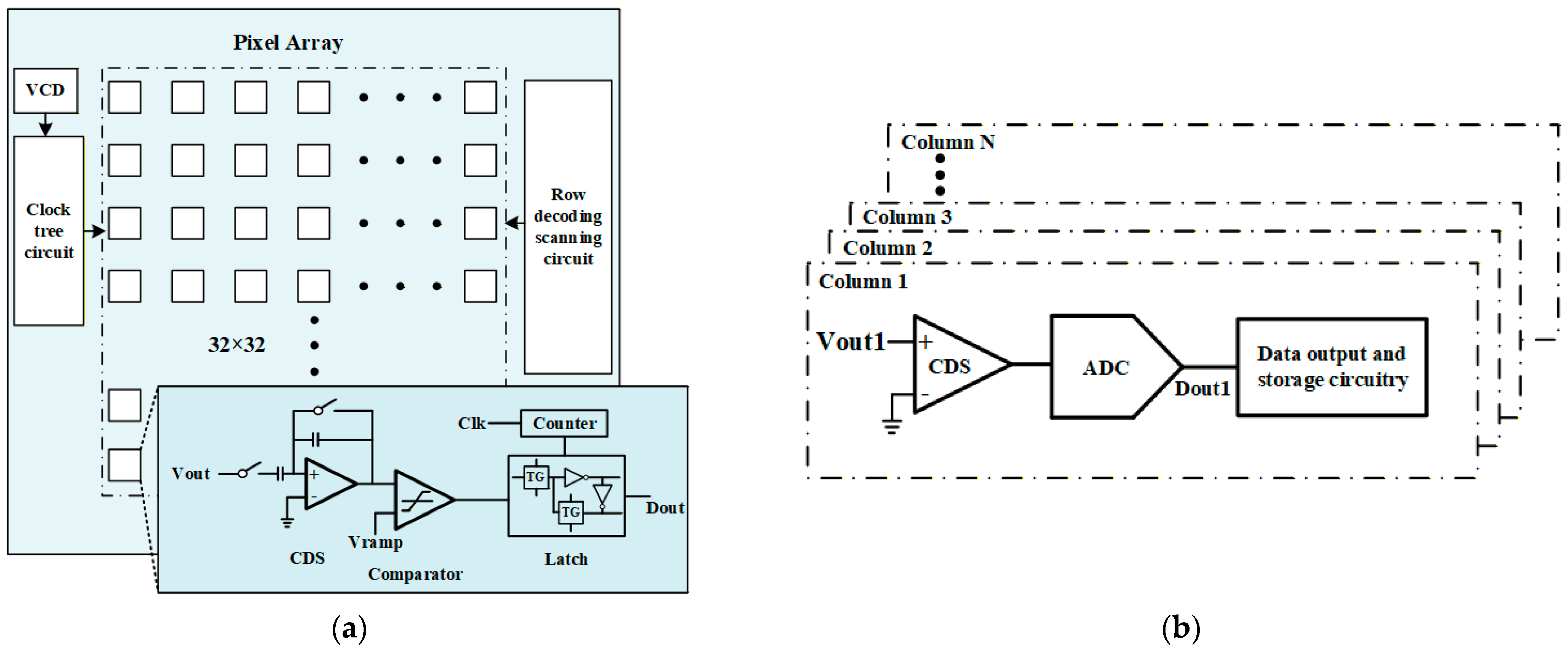
Figure 1a presents the circuit structure of the 32 × 32 × 4 pixel array CMOS image sensor. It comprises a pixel array, a voltage-controlled delay (VCD) circuit, a clock tree, a row decoding scanning circuit, correlated double sampling (CDS) circuits [
30,
31], and an ADC readout circuit. The readout circuit employs a column parallel readout method, as shown in
Figure 1b.
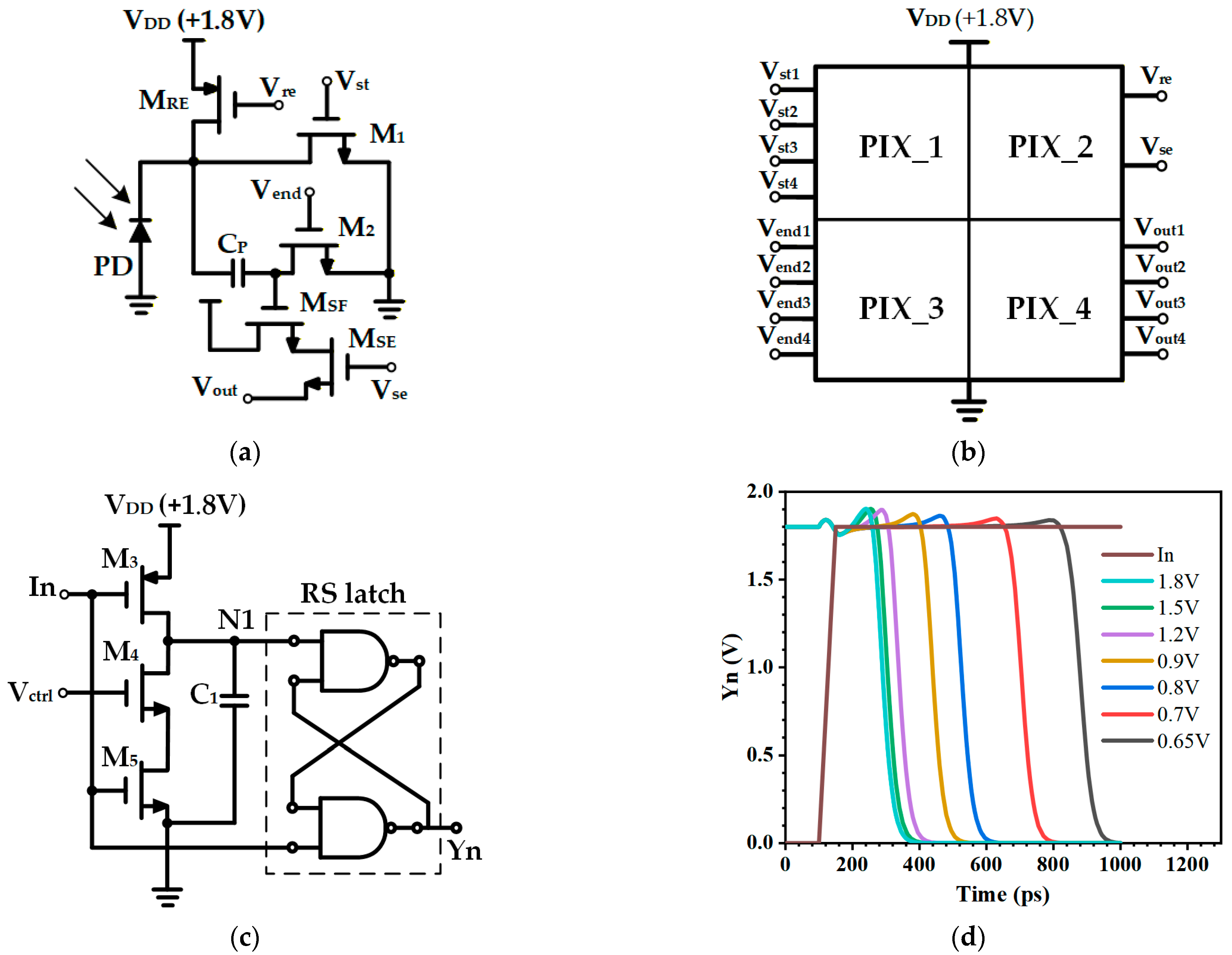
The pixel unit circuit of the sensor utilizes a 5T pixel structure, as depicted in
Figure 2a. Here, PD represents the photodiode, and C
p serves as the storage capacitor for the exposure signal. Transistors M
1 and M
2 respectively control the start and end of the exposure. M
RE functions as the reset transistor, while M
SF and M
SE are used for signal buffering and gating. V
re is the reset signal, V
st and V
end are respectively the control signals for the start and end of exposure, V
se is the output gating signal, and V
out is the output voltage signal. The four-frame pixel unit designed in this paper is shown in
Figure 2b. One pixel unit contains four independent sub-pixels. Each sub-pixel has independent V
st and V
end signals to control the start and end of exposure. All sub-pixels perform reset and gating operations synchronously. Therefore, this structure can realize synchronous reset and parallel readout. It solves the problem of long delay caused by excessive capacitors in the pixel. It achieves framing imaging while improving the temporal resolution.
The working process of the pixel unit circuit illustrated in
Figure 2a is as follows, prior to the trigger, V
re is set to ground to reset the circuit. V
re, V
st, and V
end are set to V
DD, while V
se is set to ground. In this state, M
1 and M
2 are conducting, whereas M
RE and M
SE are nonconducting. The photocurrent corresponding to the incident light on the PD flows to the ground through M
1. When exposure begins, V
st transitions to ground, making M
1 nonconducting. The current generated by the PD charges the C
p, storing the signal charge. After a certain period, V
end is set to ground, concluding the exposure. At this point, all transistors are in a nonconducting state. The charge stored in C
p is held, marking the end of the exposure process. The interval between the start and end signals constitutes the exposure time for signal acquisition. Following exposure, V
re is set to ground, causing M
RE to conduct and pull the positive terminal of the PD to V
DD. At this point, a voltage signal ready for readout is established at the gate of M
SF. Subsequently, V
se can be set to V
DD, activating M
SE to output the pixel signal. After the signal is read out, the M
RE, V
st, V
end, and V
se signals are controlled so that M
SF and M
SE are nonconducting and M
RE is conducting. The pixel unit circuit is thus reset, awaiting the next acquisition cycle.
The VCD circuit in
Figure 2c generates signals to control the start and end of exposure. It also regulates exposure time through voltage adjustment. It consists of a PMOS transistor M
3, NMOS transistors (M
4 and M
5), a capacitor C
1, and an RS flip-flop. Here, In represents the trigger-on signal for the control delayer, V
ctrl denotes the gate voltage control signal of M
4, and Yn is the output signal. As shown in
Figure 2d, the delay time of the output signal Yn varies with V
ctrl. The shutter speed can be adjusted by setting different control voltages.
The clock tree circuit utilizes a binary clock tree structure. It ensures precise clock signal distribution, synchronizing the start and end of exposure across the entire pixel array. This prevents uneven brightness between rows or columns caused by timing deviations and minimizes signal crosstalk. The row decoding scan circuit provides the selection Vse signal.
Currently, the main column-level ADC circuits applied in CMOS image sensors include SSADC, SAR ADC, and cyclic ADC. SSADC has significant advantages in power consumption, chip area, and circuit complexity. The high temporal resolution of the ultrafast four-frame CMOS image sensor designed in this paper is mainly determined by the pixel module. It can realize four-frame imaging with only one single-shot exposure. After the exposure is completed, the sampled signals are stored in the capacitors. The readout is then carried out row by row using the column-parallel readout method. Therefore, the sampling rate of the ADC circuit does not have high requirements. As a result, SSADC is selected as the column-level ADC readout circuit in this paper. The circuit is designed with a readout resolution of 12 bits, and an input analog signal range of 0–1 V.
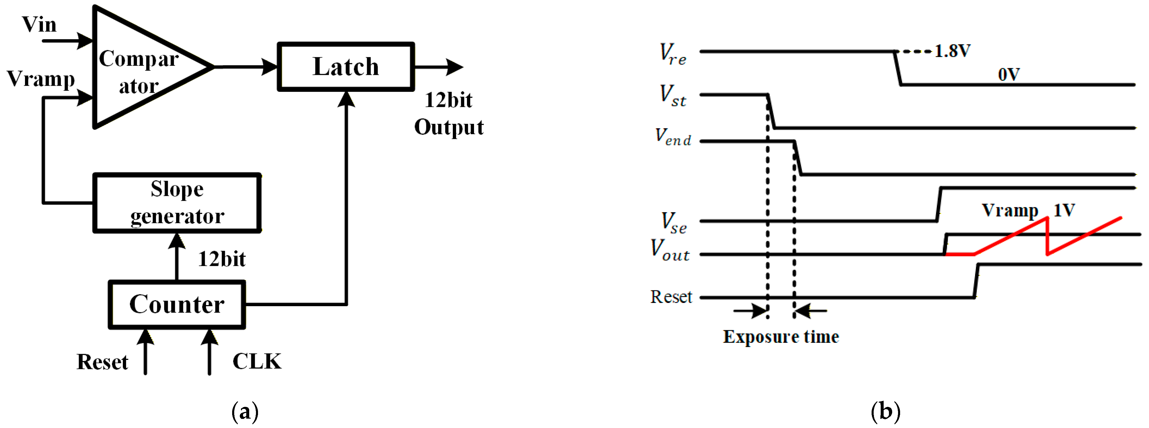
The SSADC architecture in
Figure 3a comprises a counter, a slope generator, a comparator and latch circuits. Upon the reset signal transitioning from low to high, the clock signal CLK drives the counter. The counter outputs a 12-bit signal that control the ramp generator, producing a 0–1 V Vramp signal. The output voltage of the pixel circuit is processed by the CDS circuit to eliminate fixed pattern noise, and the voltage Vin is thus obtained. The pixel output voltage Vin is then compared with Vramp through the comparator circuit. While the Vramp signal is greater than the Vin value, the comparator output voltage reverses to control the latch to hold the counter code value at that time, resulting in a 12-bit digital output.
Figure 3b shows the timing sequence of the sensor.
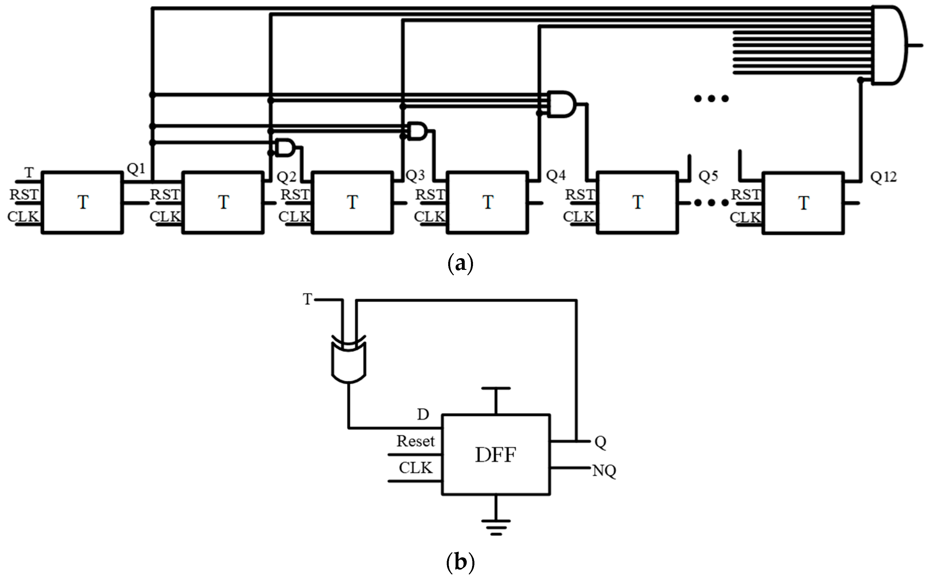
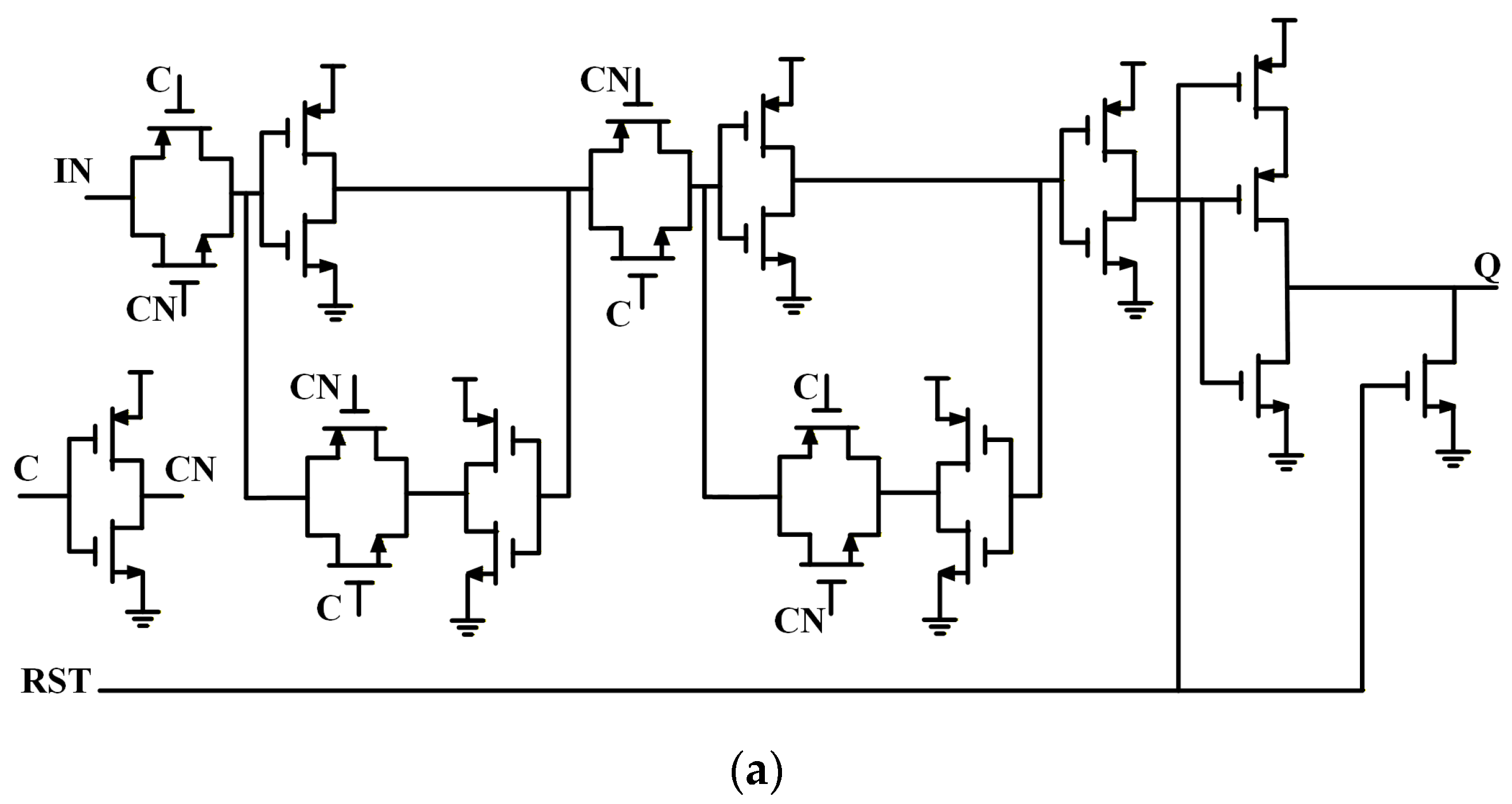
This work employs a synchronous parallel adder counter. The counting pulse served as the global clock signal is connected simultaneously to the clock inputs of all flip-flops. Consequently, all active flip-flops toggle synchronously to enable a higher counting speed. Furthermore, the excitation signal propagates to higher-order flip-flops with a delay equivalent to a single logic gate, which can keep the conversion time of each output signal highly consistent and is suitable for higher clock frequencies. The overall circuit block diagram of the counter is shown in
Figure 4a. Additionally, a reset function is designed. The T flip-flop is implemented using a D flip-flop with reset and set functions, as shown in
Figure 4b.
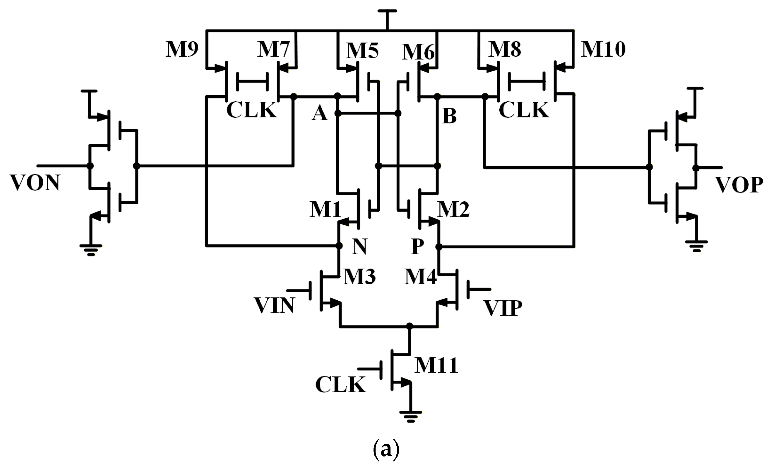
The comparator in this paper employs a dynamic latch comparator, as illustrated in
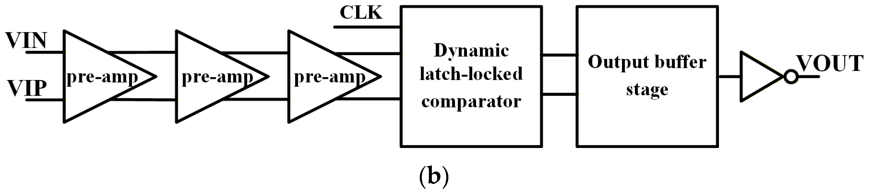
Figure 5a. When the control clock CLK is low, the comparator enters the reset phase. Transistors M7, M8, M9, and M10 turn on, resetting output nodes A and B to a high level. While CLK transitions high, the M7, M8, M9, and M10 transistors turn off. Nodes N and P discharge at different rates depending on the differential input voltage. Once the voltage difference between N and P becomes sufficient, the cross-coupling positive feedback mechanism composed of M1, M2, M5, and M6 transistors is triggered. Consequently, one node is rapidly regenerated to a high level while the other is pulled to a low level, finally yielding the comparison result. To mitigate the high input offset voltage in a dynamic latch comparator, a three-stage preamplifier is introduced preceding the comparator. This stage utilizes an input offset storage technique to reduce the offset voltage. Furthermore, an output buffer stage is added to suppress clock noise at the output. The diagram of the comparator is shown in
Figure 5b.
The slope generator circuit is based on a 12-bit current-steering digital-to-analog converter (DAC), as shown in
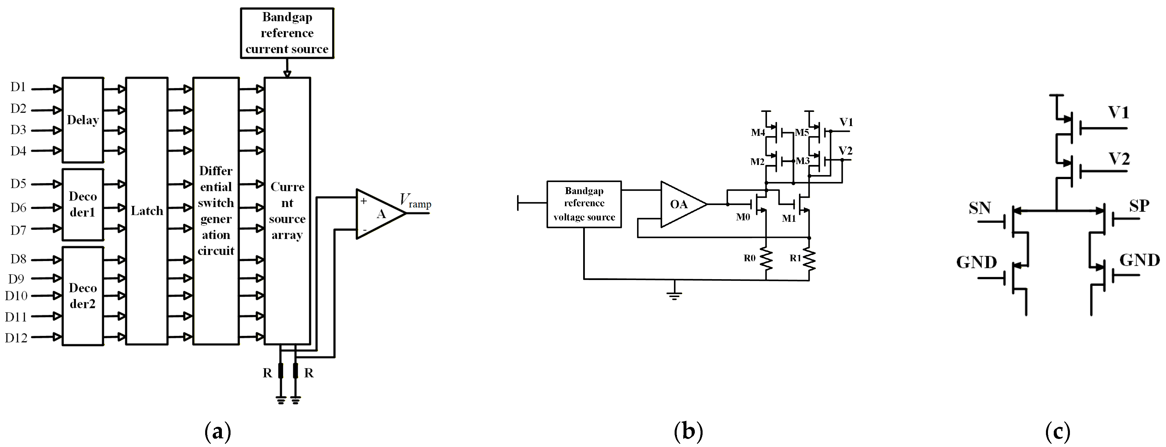
Figure 6a. The architecture comprises a decoder, delay circuits, latch, differential switch drivers, a bandgap reference current source, and a current source array. The ramp signal is generated directly across a load resistor, bypassing output buffers. This configuration ensures a high slew rate and offers better area efficiency than resistor or capacitor networks. To reduce the mismatch caused by the large current steps, a segmented architecture combining binary and thermometer coding is employed. Specifically, the four least significant bits (LSBs) use binary coding. The three intermediate bits and five most significant bits (MSBs) are converted to thermometer codes to control the current source array.
To derive the bandgap reference current, a bias voltage generation circuit is designed to bias the current source array and establish the corresponding current weight. As shown in
Figure 6b, this circuit comprises a bandgap reference voltage source, an operational amplifier, an auxiliary fine-tuning bias circuit, and a main bias circuit. In this design, R0 and R1 are external precision resistors. The inverting input terminal of the operational amplifier is connected solely to R1. Together with M1, M3 and M5, it forms the main bias circuit. These transistors constitute a low-voltage common source and common gate current source, respectively, designed to increase the output swing. The bias of the common gate transistor M3 is provided by a current source composed of M2 and M4. By adjusting R0, M3 can be biased at an appropriate voltage level. Since M0 is driven by a high-gain operational amplifier under negative feedback, the voltage at the drain of M0 remains highly stable. Consequently, the bias voltage V2 is stable, while V1 is determined by the reference current flowing through R1. When the reference current is constant, V1 also remains highly stable. The bias circuit reveals that both V1 and V2 have passed through the common source and common gate structure. As a result, the output impedance at V1 and V2 is very large, and the power supply rejection ratio is very high.
The mismatch of the unit current source and the yield of the current-steering DAC are closely linked to the area of the current source transistor. The relationship between the relative variance of t mismatch and the active area is expressed in Equation (1). Increasing the unit current source area and the overdrive voltage can reduce the mismatch. Consequently, an overdrive voltage of 500 mV is used for this design. The relationship between the relative standard deviation of the mismatch and the overall yield of the DAC is given by Equation (2).
A yield of 99.7% corresponds to a C value of 2.8. Then, the minimum area WL of the unit current source for the DAC is approximately 25.5 μm
2. The unit current source is designed to be 977.246 nA. The current I of the MOS transistor in the saturation region can be expressed as
Furthermore, the width-to-length ratio of the PMOS transistor for the unit current source is
In this paper, the current source dimensions are set to W = 2 μm, and L = 17 μm. A high output impedance can improve the DAC performance. To increase the output impedance of the current source, a cascode structure is employed as the unit current source circuit. The schematic of the unit switched current source is shown in
Figure 6c. The SN and SP signals control the switching transistors, while the GND signal biases two normally open PMOS transistors to reduce the switching noise of the current source.
The register circuit shown in
Figure 7a employs two level-sensitive latches to construct a master-slave rising-edge D flip-flop. The RST signal functions as an active-high asynchronous reset.
Figure 7b illustrates the latch and the differential switch driver with low crossing-point control. The circuit section on the left generates a differential switching signal controlled by the clock. This signal is then processed by the low crossing-point generation circuit on the right. This mechanism ensures that the current source is not in a completely off state and reduces the switching noise.
3. Results and Analysis
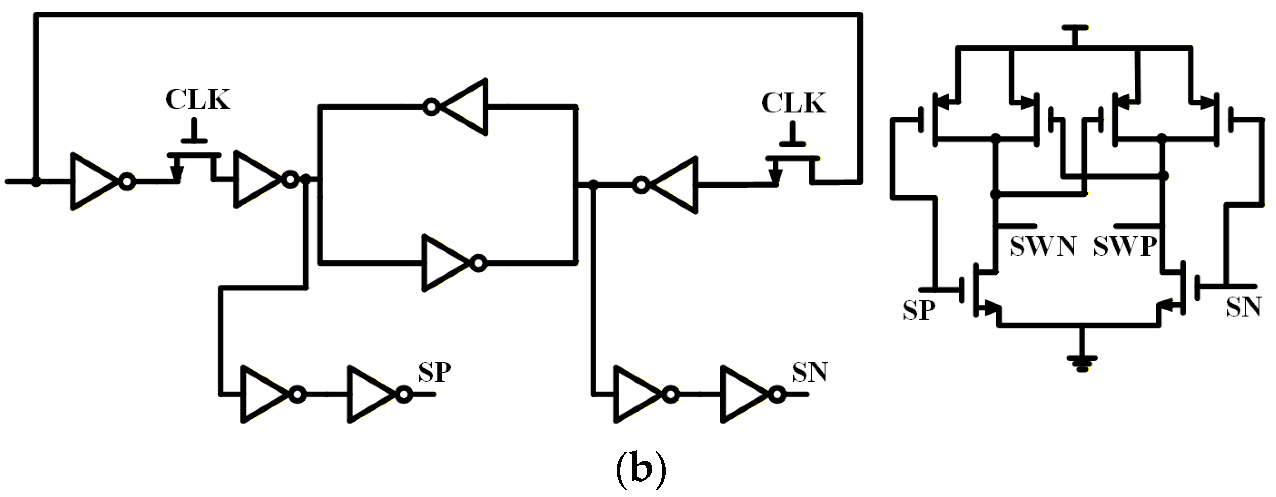
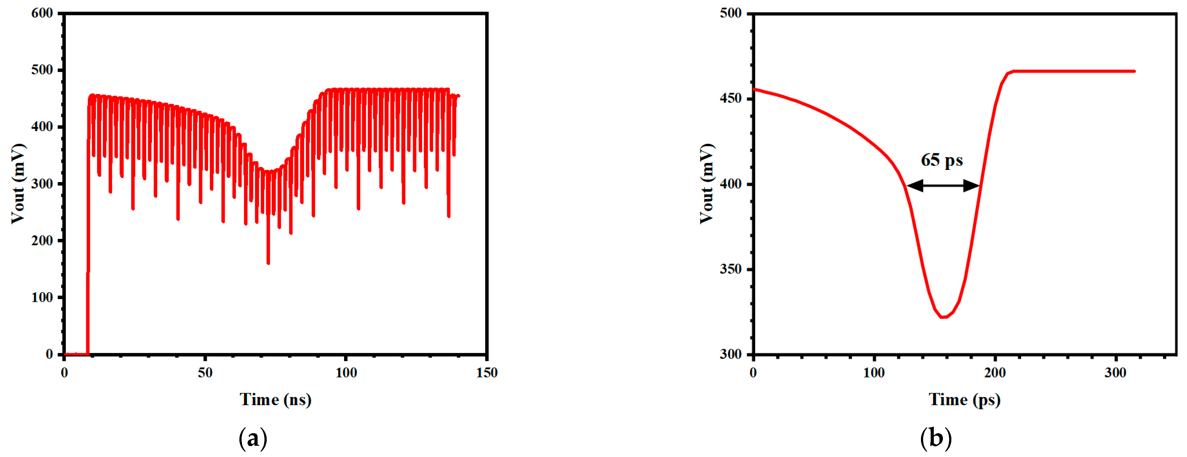
To evaluate the temporal resolution, an 8 × 8 pulse current source signal array was applied to the pixel array. Each pulse current source signal was set to 10 mA, and a pulse width of 5 ps. The center distance between adjacent pulses was set to 5 ps. This configuration establishes a temporal scale range from 0 to 315 ps with a 5 ps resolution. Row and column decoder scan circuit provide the selected signal needed for each pixel. The exposure time is regulated by the VCD circuit, and the timing diagram of the pixel array signal scanning and reading data is shown in
Figure 8a. This result was obtained by sequentially scanning the 64 selected signals. When the pulse current signal falls outside the exposure time window, the pixel circuit outputs a baseline voltage of 466 mV. The scan output voltage is reduced only while the pulse current signal synchronizes with exposure time.
The scanning output signal from
Figure 8a is converted into the time resolution curve, as shown in
Figure 8b. The full width at half maximum (FWHM) of the curve represents the temporal resolution capability for each frame of the sensor, which is 65 ps.
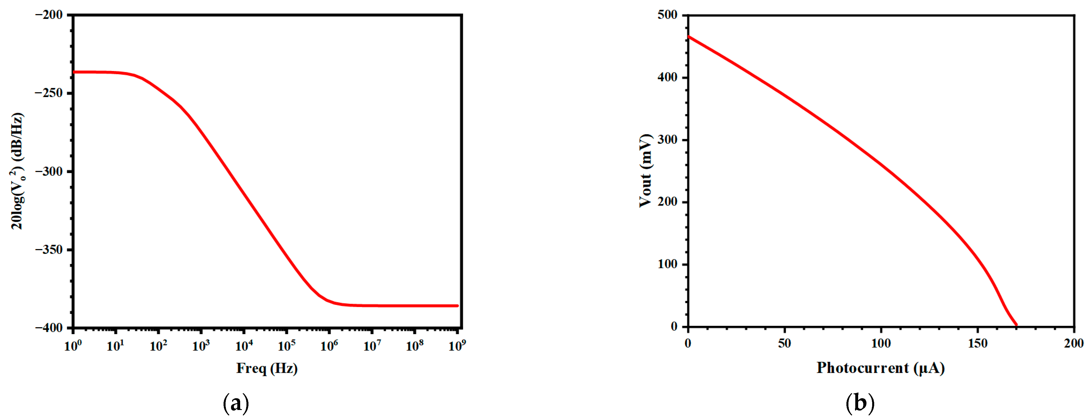
The output noise of the pixel circuit was simulated. The power spectral density curve of the output noise is shown in
Figure 9a. The total output noise is measured to be 77.47 μV. In the low frequency band, 1/f noise is the dominant component. In the high frequency band, thermal noise is the main contributor.
Fix the exposure time at 100 ps, adjust the magnitude of the incident photocurrent, and simulate the output voltage of the pixel circuit. The relationship between the output voltage of the pixel circuit and the input photocurrent is shown in
Figure 9b. It can be concluded that the output voltage of the 5T pixel designed in this paper decreases with the increase in the input photocurrent. The circuit achieves an output swing of 466 mV, with a detectable photocurrent range of 0–170 μA.
The expression for the dynamic range (DR) is:
Among them, |Vout − Vdark|max represents the maximum output swing of 466 mV, and Vnoise denotes the output noise of 77.47 μV. Consequently, the dynamic range can be calculated to be 75.6 dB.
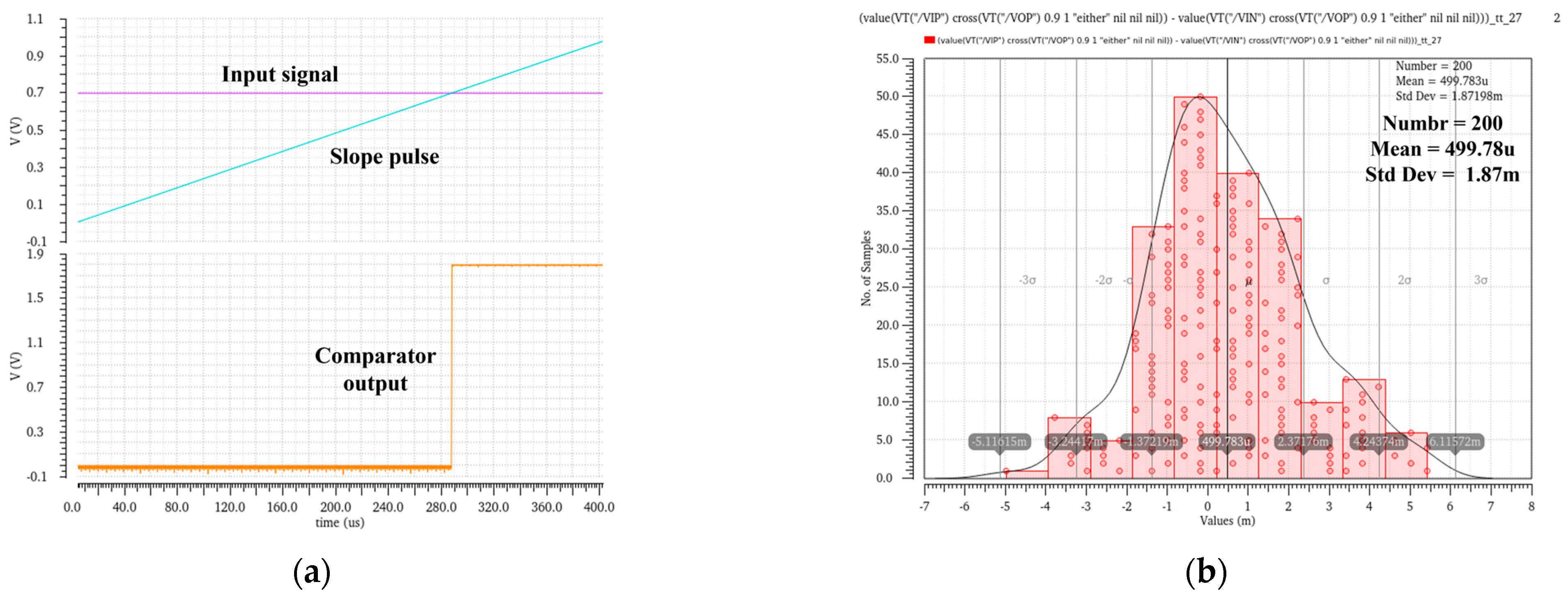
The comparator output is shown in
Figure 10a. The comparator output transitions while the slope signal exceeds the input signal. The offset voltage simulation is shown in
Figure 10b, with a mean offset voltage of 0.5 mV and a standard deviation of 1.87 mV.
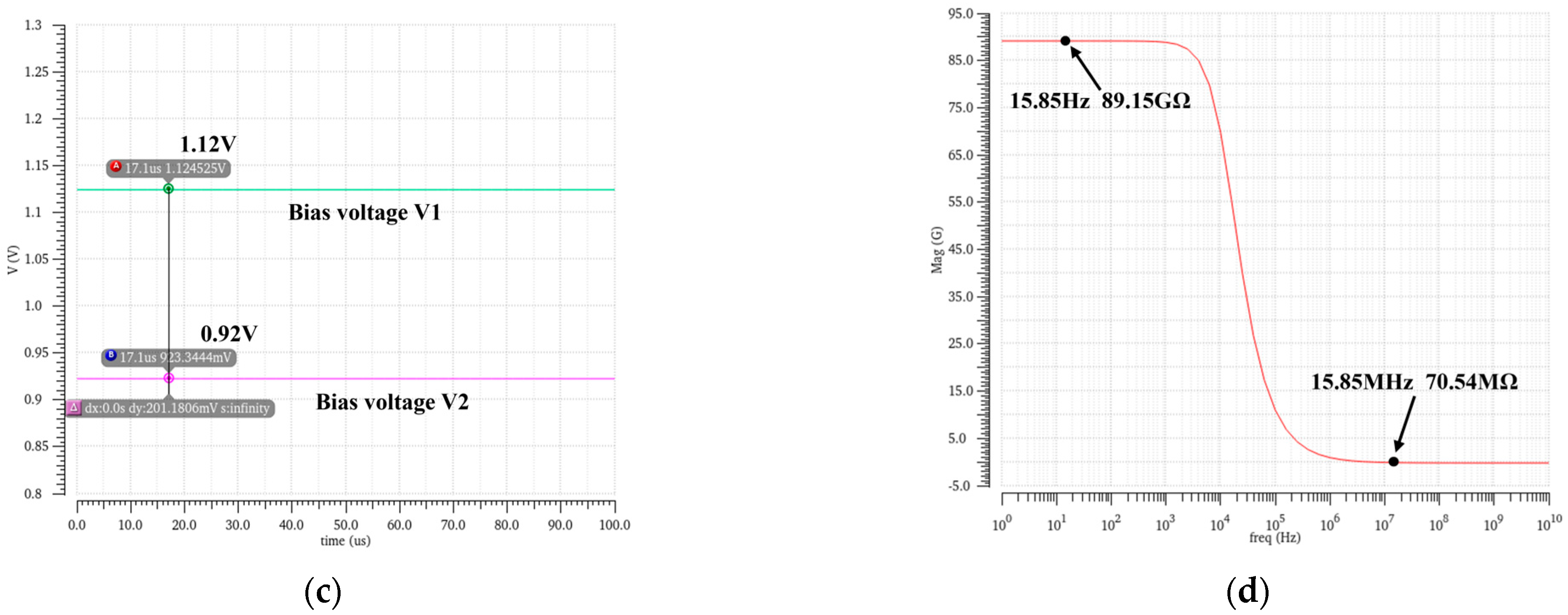
Figure 10c shows the signals V1 and V2 output from the bias voltage generation circuit of the bandgap reference current source. Both of the two signals remain highly stable over time. The output impedance of the reference current source is presented in
Figure 10d. It achieves 89 GΩ at low frequencies and maintains tens of MΩ at high frequencies.
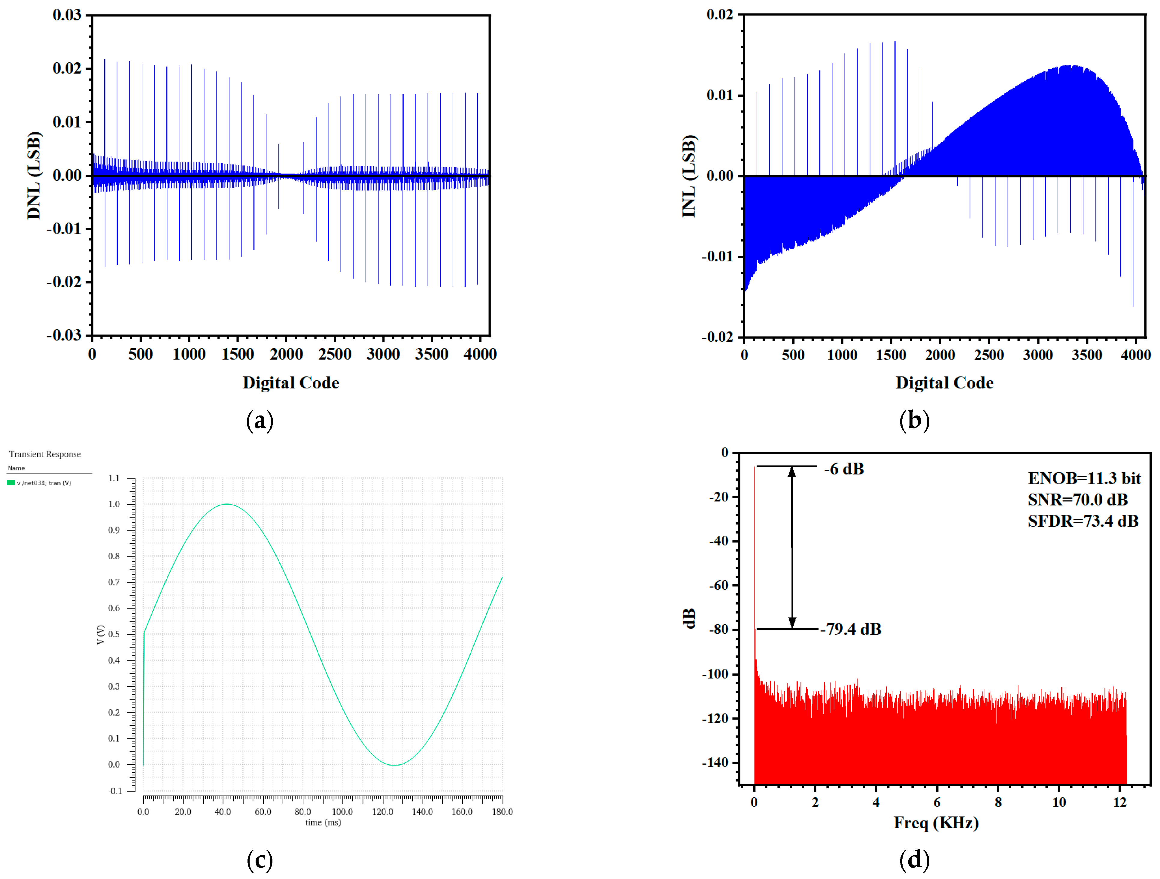
The slope pulse generator outputs a differential signal ranging from 0 to 500 mV. After it passes through the differential operational amplifier, a slope pulse ranging from 0 to 1 V is obtained. The differential nonlinearity (DNL) and integral nonlinearity (INL) of the final slope signal are shown in
Figure 11a,b, respectively. Both of them remain within ±0.03 LSB, demonstrating an excellent linearity.
Power consumption simulation is carried out on the above-mentioned SSADC circuit. The average current flowing through the power supply is recorded as 5.15 mA at a 1.8 V supply voltage, and the power consumption of the SSADC circuit is thus calculated to be 9.3 mW.
The dynamic characteristics of the SSADC were simulated by connecting an ideal 12-bit DAC to the ADC output to reconstruct the analog signal for analysis. With a sampling frequency of 24.41 kS/s and an input sinusoidal frequency of 5.96 Hz, the reconstructed waveform from the ideal DAC is shown in
Figure 11c. The spectral graph of the output signal obtained by FFT transformation of the output result is shown in
Figure 11d. The SSADC achieves an effective number of bits (ENOB) of 11.3 bits, a spurious free dynamic range (SFDR) of 73.4 dB, and a signal-to-noise ratio (SNR) of 70.0 dB.
The performance characteristics and simulation results of the designed SSADC, together with the comparison with previous ADC research works for CMOS image sensor applications, are summarized in
Table 1.
Compared with the previous SSADCs applied to CMOS image sensors, the SSADC designed in this paper has significant advantages in terms of ENOB and SNR. It can provide higher quantization accuracy for the CMOS image sensor, which is of great significance for the accurate reconstruction of the dynamic process in ICF experiments. The CMOS image sensor designed in this paper realizes single-shot exposure four-frame imaging, so it has no strict requirement on the quantization speed of the ADC. However, the designed SSADC still has the limitations of lower sampling frequency and higher power consumption. In the subsequent research, we will improve the sampling frequency and reduce the power consumption by increasing the main clock frequency, adopting more advanced CMOS processes, and optimizing the circuit design.