


Abstract
The 795 nm wavelength corresponds to the D1 transition of rubidium atoms and is widely used in atomic optical pumping, atomic clocks, magnetometers, and precision spectroscopy. For compact free-space collimation, beam shaping, and efficient fiber coupling, edge-emitting semiconductor lasers with reduced fast-axis (vertical) divergence are highly desirable, yet low-divergence designs at 795 nm remain limited. Here, we propose and demonstrate low-divergence photonic-crystal epitaxy (LD–PC) for 795 nm edge-emitting lasers. By engineering a periodic n-side photonic-crystal stack to place the fundamental vertical mode near the photonic band edge, the vertical mode is expanded while maintaining effective modal discrimination. Narrow-ridge Fabry–Pérot lasers based on GaAsP/AlGaAs single-quantum-well epitaxy were fabricated and characterized. The optimized LD–PC device (3 μm ridge width, 1 mm cavity length) delivers 227 mW at 200 mA with a threshold current of 23 mA, a slope efficiency of 1.28 W/A, and a peak wall-plug efficiency of 55% under continuous-wave operation at 25 °C. The measured far-field divergences (FWHMs) are 7.16° and 18.83° in the lateral and vertical directions, respectively, corresponding to a reduction in the vertical divergence from >40° in the reference structure to <20° with LD–PC. These results validate photonic-crystal epitaxy as an effective route toward compact, high-performance, low-divergence 795 nm semiconductor laser sources for rubidium-based atomic systems.
1. Introduction
The spectral region around 795 nm corresponds to a key wavelength near the D1 transition line of the alkali-metal rubidium (Rb), and thus plays an essential role in atomic optical pumping, atomic clocks and magnetometers, and precision spectroscopic metrology [1,2]. For these system-level applications, edge-emitting semiconductor lasers are among the preferred light sources due to their compact footprint, high electro-optical efficiency, and ease of integration. In practical scenarios such as free-space beam collimation, lens-based beam shaping, and fiber coupling, a small far-field divergence is particularly desirable, as it can reduce optical packaging complexity and improve coupling efficiency [3,4,5,6,7]. To suppress far-field divergence, especially the vertical far-field divergence of laser diodes, two representative approaches are commonly adopted. The first relies on large optical cavity (LOC) or ultra-LOC epitaxial designs, which reduce the waveguide refractive-index contrast and expand the optical mode size [8]. The second introduces photonic crystal epitaxy or mode-expansion layers to further enlarge the optical mode while maintaining a reasonable confinement factor [9,10,11]. However, the divergence reduction enabled by LOC designs is not unlimited. When the waveguide thickness exceeds a certain level, higher-order modes may lase, leading to degraded beam quality and compromised device performance [12,13,14]. In comparison, incorporating a periodic photonic-crystal epitaxial layer can achieve a larger vertical mode size and a lower vertical far-field divergence without significantly sacrificing the optical confinement factor or incurring excessive electrical loss.
For semiconductor lasers in the 700-800 nm band, 780 nm and 795 nm devices have been widely investigated as representative platforms for high-power and narrow-linewidth applications, respectively. Nevertheless, their vertical (fast-axis) far-field divergence typically remains relatively large, commonly in the range of 30–40°. In 2021, He et al. [15] demonstrated a 780 nm laser diode delivering an output power of 10.1 W, and in 2023, Li et al. [16] from the same institute designed and fabricated a 780 nm laser diode employing an asymmetric large-optical-cavity structure, achieving 16 W output power. For these two devices, the vertical divergence angles (defined by 95% energy) were 46° and 45°, respectively. In 2024, Wang et al. [17] reported a 780 nm laser diode with a 71% wall-plug efficiency, while the vertical far-field divergence (FWHM) remained as large as 40°. Notably, Xu et al. [18] introduced a photonic-crystal epitaxy and reduced the vertical divergence of a 780 nm laser to 21°. In contrast, low-divergence designs have not been widely implemented for 795 nm edge-emitting semiconductor lasers. In 2021, narrow-ridge 795 nm edge-emitting lasers were reported with output powers of 50–100 mW, yet no divergence characteristics were provided [19,20]. In 2023, a narrow-ridge 795 nm edge-emitting laser was demonstrated with a reported vertical far-field divergence of 43° [21]. Although substantial progress has been achieved for 780 nm edge-emitting semiconductor lasers in terms of output power, efficiency, and divergence control, corresponding low-divergence designs for 795 nm devices remain limited. Previously reported 795 nm edge-emitting lasers have mainly focused on narrow-ridge operation or DFB-based wavelength selectivity, whereas systematic reduction in the vertical far-field divergence has rarely been demonstrated.
Motivated by these limitations, this work proposes a low-divergence photonic-crystal epitaxy (LD–PC) design for 795 nm edge-emitting lasers. A photonic-crystal layer is introduced on the n-side of the epitaxial structure, and mode-matching engineering is employed to enable a controllable vertical expansion of the fundamental mode, thereby reducing the vertical far-field divergence. For narrow-ridge devices, the impacts of ridge width and etching depth on cross-sectional modal distributions are systematically investigated to realize a ridge design supporting single cross-sectional mode operation (mode confinement factor ratio > 2). Finally, high-performance narrow-ridge lasers are fabricated and tested. The far-field divergence of the proposed LD–PC design is benchmarked against that of 795–PC and the reference 795–Base. Through optimization of the photonic-crystal epitaxy design, the vertical divergence is reduced by approximately 50%, establishing a practical approach for realizing low-divergence 795 nm edge-emitting semiconductor lasers. Above all, the present work addresses an important gap by introducing a low-divergence photonic-crystal epitaxy design for 795 nm lasers, aiming to simultaneously maintain narrow-ridge single cross-sectional-mode operation, relatively high output power, and significantly reduced vertical divergence.
2. Materials and Methods
2.1. Photonic-Crystal Epitaxy Model and Transfer-Matrix Formulation
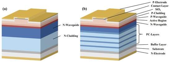
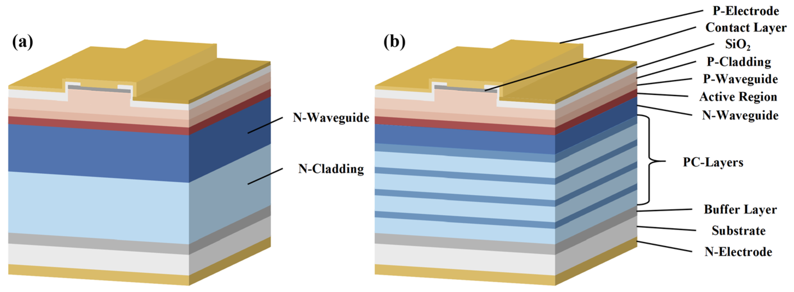
For the epitaxial design of the 795 nm low-divergence edge-emitting laser, a GaAsP/AlGaAs single-quantum-well (SQW) active region was employed. The waveguide and cladding layers were both AlGaAs alloys with different Al compositions to tailor the refractive-index profile and optical confinement. Tensile strain was intentionally introduced in the GaAsP/AlGaAs active region; as a result, the emitted laser polarization was transverse-magnetic (TM) [22,23]. An overall asymmetric waveguide configuration was adopted to reduce internal optical loss. Specifically, the p-side waveguide thickness was reduced compared with the n-side, which helps mitigate absorption-related loss while maintaining sufficient modal confinement in the active region. Figure 1 schematically illustrates the device structures that was investigated in this work: Figure 1a shows the reference laser structure without photonic-crystal epitaxy, whereas Figure 1b depicts the counterpart incorporating a photonic-crystal epitaxial layer.
Figure 1.
Schematic diagrams of the laser epitaxial structures (not to scale): (a) reference structure without a photonic-crystal layer; (b) structure incorporating photonic-crystal epitaxy.
The photonic-crystal (PC) epitaxy can be regarded as an additional n-side cladding section with a periodically modulated refractive-index profile. Each period is typically composed of a high-index layer and a low-index layer. The thicknesses of the low- and high-index layers are denoted as and , and their refractive indices are and , respectively. The corresponding period is . For the TM mode in the laser waveguide, the magnetic-field component can be written as:
where is the angular frequency and is the in-plane propagation constant, with being the free-space wavenumber and is the effective refractive index of the guided mode. In a one-dimensional layered medium along the vertical direction , the electric-field components can be directly expressed in terms of :
where denotes the spatially periodic permittivity distribution within the PC epitaxy layer. According to Bloch’s theorem, the field in a periodic medium satisfies:
The is a periodic envelope function and is the Bloch wavevector along the vertical direction. To enforce the continuity conditions at material interfaces, the TM-mode state vector at position is defined as:
By combining Bloch periodicity, one obtains:
For a single-period photonic crystal structure, the transfer-matrix method gives:
where is the transfer matrix, determined by the material indices (, ) and thickness (, ). Assuming that the high-index layer is placed below the low-index layer, consistent with the epitaxial stacking order, the single-period matrix can be written as:
Here, , and permittivity , where is the in-plane propagation constant of the guided mode, and is the vacuum permittivity. Combining the Bloch periodicity (6) relation with transfer matrix (7), is obtained as an eigenvalue of . For a lossless photonic-crystal structure (), the Bloch dispersion can be written as:
When , the Bloch wavevector is real and the wave can propagate through the periodic stack, corresponding to a pass band. In contrast, when , results in an evanescent decay in the periodic medium with an approximate penetration depth . This criterion enables the determination of the photonic pass/stop bands for a given wavelength and propagation constant. In the present design, the PC parameters were selected such that the vertical fundamental mode lies close to (or partially approaches) the band-edge condition, which facilitates field expansion in the vertical direction. Meanwhile, higher-order modes are engineered to fall into the pass band of the photonic-crystal stack, thereby experiencing additional leakage loss and being effectively suppressed, ultimately favoring vertical fundamental mode operation.
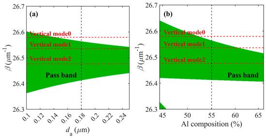
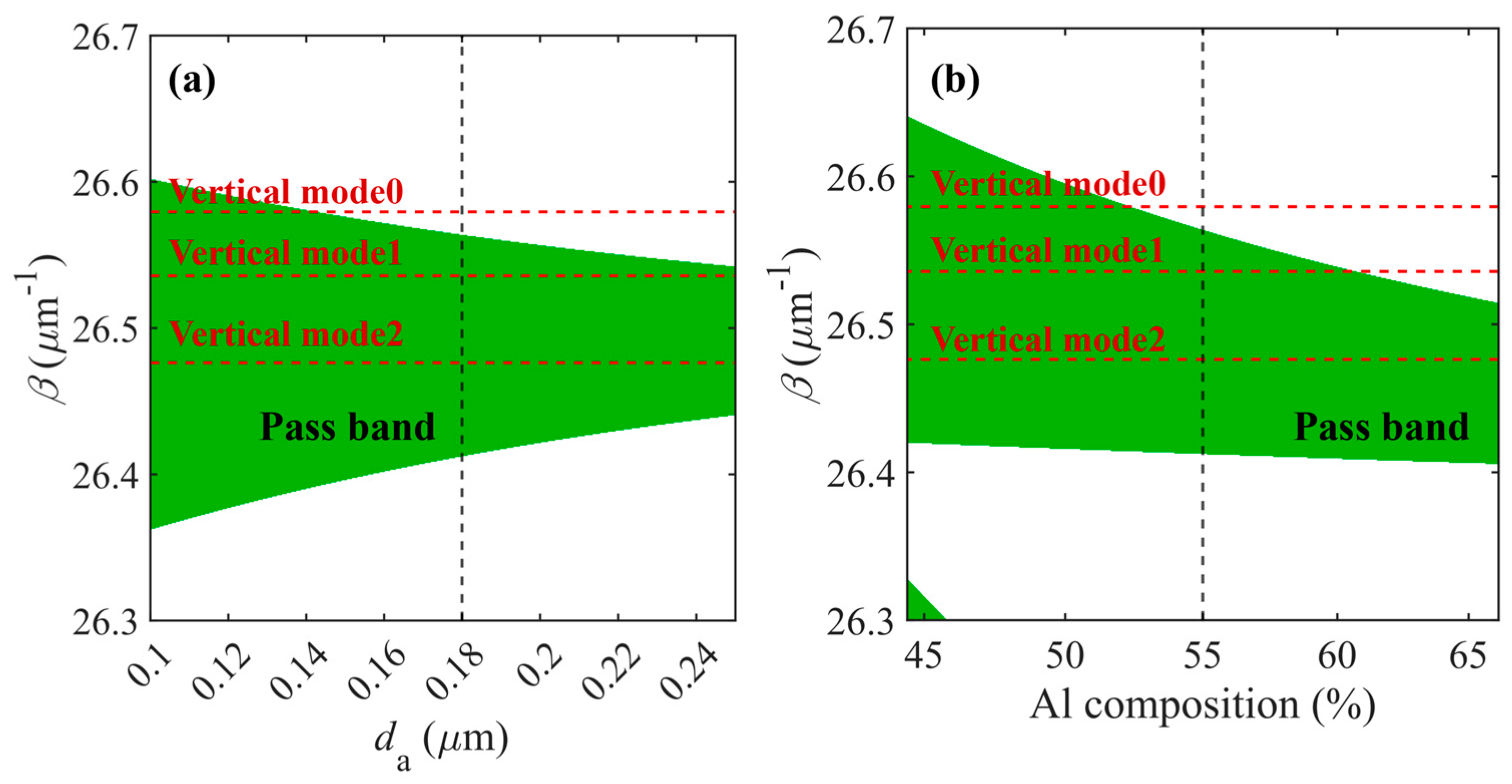
To make the LD–PC design process more explicit, the photonic band structure of the vertical PC stack was analyzed as a function of the key parameters of the low-index layer, thickness da and Al composition. Figure 2 plots the calculated pass-band regions in the β-parameter space (green) together with the propagation constants of the first several vertical modes (red dashed lines) while sweeping da (Figure 2a) and Al composition (Figure 2b). The LD–PC design aims to realize a mode-selective band-edge condition rather than pushing all modes into a stop band. In the optimized design, the nominal low-index layer is chosen as an Al0.55Ga0.45As layer with da ≈ 0.18 μm (180 nm) and Al composition ≈ 0.55 (55%), where the fundamental vertical mode is intentionally placed close to the band edge, whereas the higher-order vertical modes remain inside the pass band.
Figure 2.
Photonic band structure simulation results of the LD–PC design (green regions represent the pass bands, red dashed lines denote the propagation constants of the device modes, and vertical dashed lines indicate the nominal design point): (a) dependence on the low-index-layer thickness; (b) dependence on the composition of the low-index layer.
When the fundamental vertical mode approaches the band edge, its penetration into the PC region is enhanced, leading to an enlarged effective vertical near-field size and consequently a reduced vertical far-field divergence. In contrast, the higher-order modes located inside the pass band are more prone to propagation/leakage through the periodic stack and therefore exhibit reduced effective confinement and modal preference. Importantly, Figure 2 also indicates that the above mode ordering and near-band-edge condition is preserved within a finite parameter window around the nominal design point. Specifically, maintaining Mode 0 close to the band edge while keeping higher-order modes in the pass band can be achieved for approximately da ≈ 0.16–0.20 μm (i.e., 180 ± 20 nm) and Al composition ≈ 0.52–0.58 (i.e., 0.55 ± 0.03), suggesting a practical epitaxial growth tolerance for the low-index layer thickness and composition.
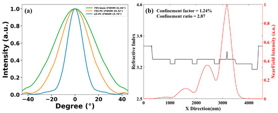
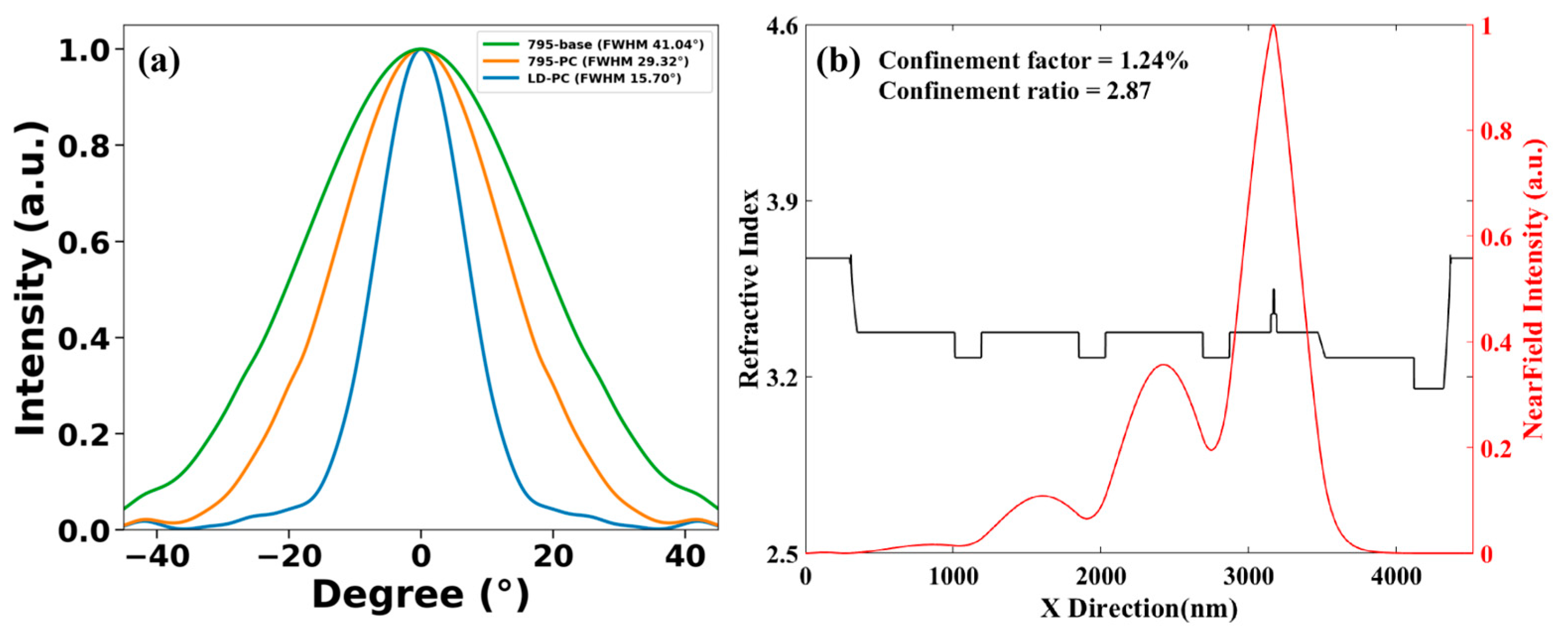
Based on the above theoretical framework, numerical simulations were performed to design the photonic-crystal epitaxy for 795 nm edge-emitting lasers. Three epitaxial structures were investigated: a reference structure without a photonic-crystal layer (denoted as 795–Base), a structure incorporating photonic-crystal epitaxy (795–PC), and a further optimized design targeting minimized vertical divergence (LD–PC). Figure 3a summarizes the simulated vertical far-field divergences (FWHMs) of the three structures, yielding 41.04°, 29.32°, and 15.70° for 795–Base, 795–PC, and LD–PC, respectively. To ensure fundamental-mode operation in the vertical direction, the photonic-crystal parameters were tuned to increase the confinement-factor ratio between the fundamental mode and the first-order mode, i.e., to enlarge the ratio of their optical confinement factors. This design strategy provides an effective degree of modal discrimination while preserving the desired mode expansion. Figure 3b shows the simulated refractive-index profile and the corresponding near-field modal distributions for the LD–PC structure. The near-field results confirm that the fundamental mode is vertically expanded into the photonic-crystal region, and the calculated confinement-factor ratio between the fundamental and first-order modes reaches 2.87, indicating a clear preference for fundamental-mode lasing.
Figure 3.
Simulation results of the photonic-crystal epitaxy: (a) vertical far-field divergence angles (FWHMs) of the 795–Base, 795–PC, and LD–PC structures; (b) refractive-index profile and near-field modal distribution of the LD–PC structure.
2.2. Cross-Sectional Mode Simulation
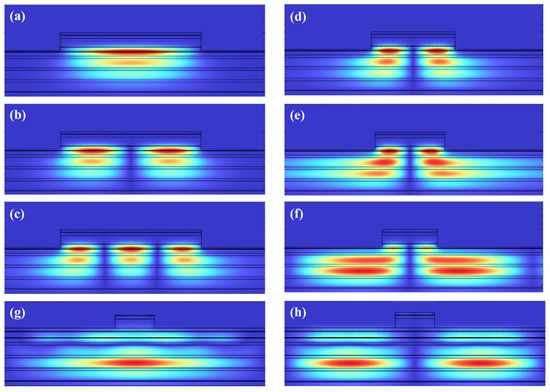
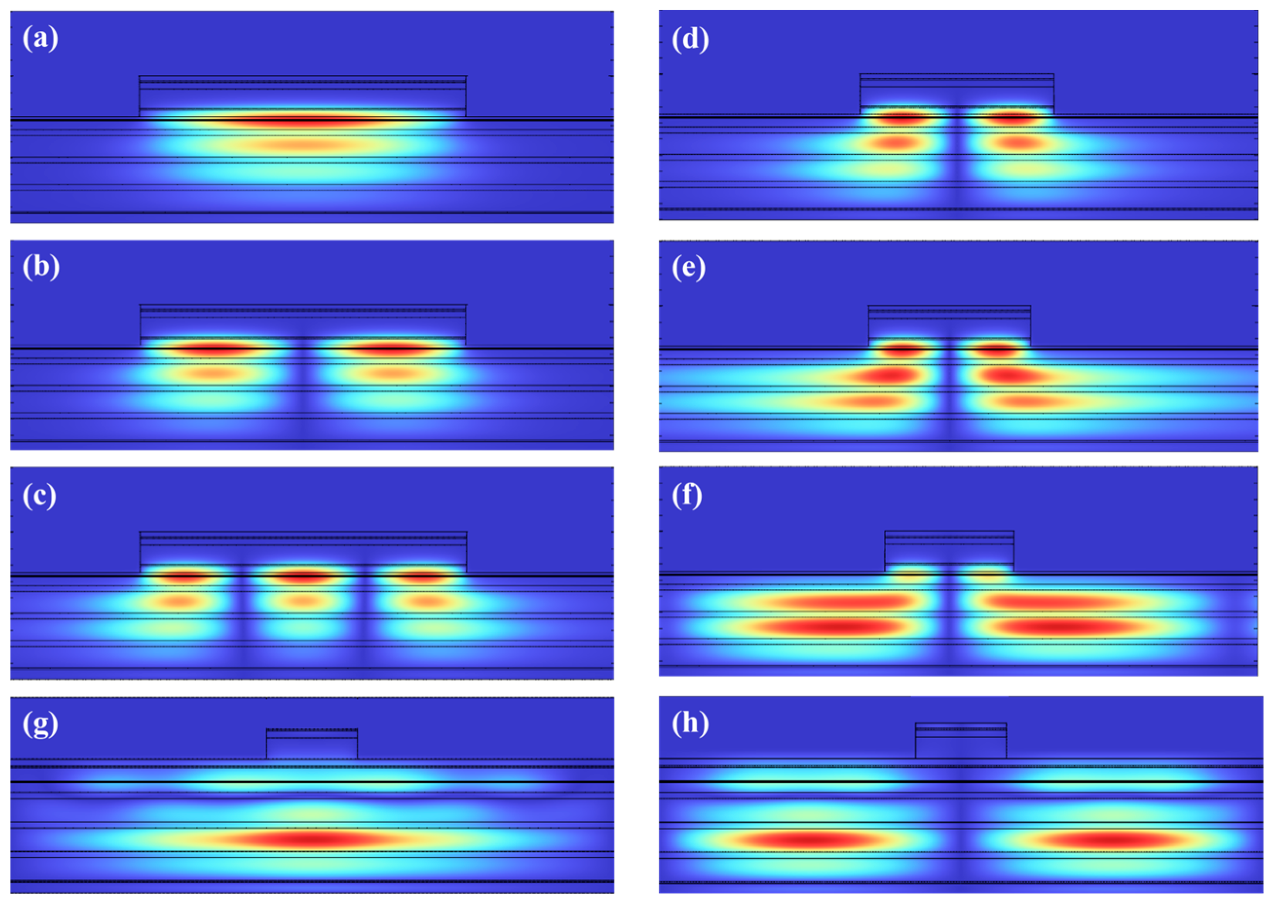
After introducing the photonic-crystal epitaxial structure, the ridge-waveguide structure was further investigated using simulations. For narrow-ridge edge-emitting lasers, higher beam quality requires both fundamental vertical-mode and fundamental lateral-mode operation [13,24]. Therefore, we analyzed the cross-sectional modes, i.e., the optical modes distributed over the ridge cross-section and formed by the coupling between vertical and lateral modal components, in order to evaluate how the ridge structure affects modal behavior. Since the device operates in the TM polarization mode, TM00 denotes the cross-sectional mode formed by the coupling of the fundamental vertical mode and the fundamental lateral mode, whereas TM10 denotes the cross-sectional mode formed by the coupling of the first-order vertical mode and the fundamental lateral mode. Similarly, TM01 and TM11 represent the cross-sectional modes formed by the coupling of the fundamental vertical mode with the first-order lateral mode, and of the first-order vertical mode with the first-order lateral mode, respectively.
The simulated distributions of the TM00–TM11 cross-sectional modes at a ridge height of 1150 nm, calculated using COMSOL Multiphysics 6.0, are shown in Figure 4a–h. For a ridge width of 10 μm, TM00, TM01, and TM02 can coexist, as shown in Figure 4a–c. However, when the ridge width is reduced from 6 μm to 4 μm, the ridge can no longer support the second-order lateral mode, while the first-order lateral mode rapidly leaks from the ridge region into the adjacent lateral areas, as shown in Figure 4d–f. Figure 4g,h show the cross-sectional distributions of the TM10 and TM11 modes. Among them, TM10 has already been effectively suppressed by the epitaxial design itself since the confinement-factor ratio between the fundamental and first-order vertical modes is greater than 2.
Figure 4.
Two-dimensional cross-sectional mode simulations. (a–f) Simulated lateral-mode profiles under an etch depth of 1150 nm for wide and narrow ridges: (a) TM00, (b) TM01, and (c) TM02 for a 10 μm ridge; TM01 for ridge widths of (d) 6 μm, (e) 5 μm, and (f) 4 μm. (g) TM10 and (h) TM11 mode profiles for a 3 μm ridge. The color scale in each panel now indicates the normalized optical field intensity, with red/yellow representing higher intensity and blue representing lower intensity.
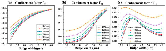
To further evaluate modal competition inside the device, the confinement factors of the TM00, TM01, and TM11 cross-sectional modes, denoted as , and , respectively, were calculated for different ridge geometries, as shown in Figure 5. It can be seen that, with increasing ridge height from 1000 nm to 1250 nm, the confinement factors of all three modes exhibit an overall decreasing trend. However, once the ridge height reaches approximately 1200 nm, the marginal reduction effect becomes much less pronounced with further increases in ridge height. With respect to ridge width, TM00 and TM01 show similar tendencies, namely that both and decrease monotonically as the ridge width decreases, as shown in Figure 5a,b. Among them, decreases much more rapidly and approaches zero in deeply etched (>1200 nm) narrow-ridge (<3.5 μm) structures.
Figure 5.
Calculated confinement factors of the cross-sectional modes as function of ridge width (3–6 μm) for etch depths from 1000 to 1250 nm: (a) confinement factor of TM00; (b) confinement factor of TM01; (c) confinement factor of TM11.
For the TM11 mode, the confinement factor exhibits a non-monotonic dependence on ridge width, first increasing and then decreasing, i.e., an inverted-U-shaped trend, as shown in Figure 5c. This indicates that, at very small ridge widths, TM11 is limited by the first-order lateral component, resulting in a relatively low confinement factor. As the ridge width increases, the TM11 mode gradually becomes better established and overlaps more effectively with the active region, causing to increase. However, when the ridge width is further enlarged, the first-order lateral component continues to spread laterally, and a larger fraction of the optical field is distributed outside the active region so that decreases again. Moreover, with increasing ridge height, the overall level of decreases and this inverted-U-shaped trend becomes more pronounced, especially in the range of 1100–1250 nm. This is because the first-order vertical mode is more sensitive to the epitaxial structure than the fundamental vertical mode, and increasing ridge height enhances the perturbation to the original waveguide profile, thereby making the first-order vertical mode less favorable.
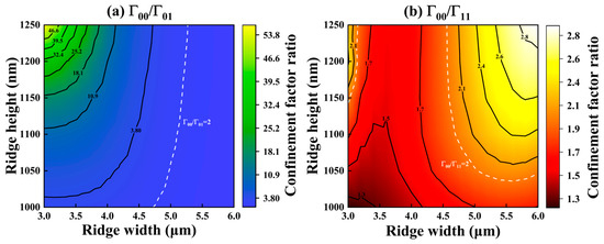
The confinement-factor ratios of TM00 relative to TM01 and TM11 were further mapped in two dimensions as functions of ridge width and ridge height, as shown in Figure 6, where the white dashed line indicates the reference condition of confinement factor ratio = 2.
Figure 6.
Two-dimensional contour maps of the confinement factor ratios as functions of ridge width and ridge height: (a) confinement factor ratio of ; (b) confinement factor ratio of . The white dashed contour indicates the reference condition of confinement factor ratio = 2.
Figure 6a shows , which increases markedly with decreasing ridge width and increasing ridge height, especially in the narrow-ridge region. This trend is consistent with the rapid lateral leakage of the TM01 mode observed in Figure 4d–f, indicating that a narrower ridge together with a deeper etch can effectively enhance the lateral refractive-index contrast and thereby promote the leakage and suppression of TM01. The contour corresponding to further shows that reducing the ridge width while increasing the ridge height enlarges the parameter region in which TM01 can be effectively suppressed. By contrast, Figure 6b shows that exhibits a non-monotonic, valley-like dependence on ridge geometry, which is consistent with the inverted-U-shaped variation of . This indicates that, under certain ridge–width and ridge–height combinations, TM11 may become the dominant competing mode to TM00, even when TM01 is already well suppressed. Therefore, both contour maps suggest that, for the LD–PC structure, a ridge width of 3 μm and an etch depth of 1200 nm represent an optimized geometry for achieving single cross-sectional-mode lasing corresponding to the coupled fundamental vertical mode and fundamental lateral mode. It should be noted that the confinement-factor ratio only quantifies the optical overlap with the active region and thus provides a trend-level guideline for modal distribution and competition. The actual lasing mode can also be affected by additional factors, including modal loss, thermal lensing, and nonuniform current injection.
3. Experiments and Results
The designed epitaxial structures were grown on n-type (100) GaAs substrates through metal–organic chemical vapor deposition (MOCVD). After epitaxial growth, ridge-waveguide stripe devices were fabricated using a standard i-line photolithography process followed by inductively coupled plasma (ICP) etching. A SiO2 insulating layer was then deposited through plasma-enhanced chemical vapor deposition (PECVD), after which, contact windows were opened for metallization. The p-side metal contact was subsequently deposited, and the wafers were thinned prior to n-side metallization. Rapid thermal annealing (RTA) was performed to alloy the contacts and form ohmic interfaces. Finally, the wafer was cleaved into Fabry–Pérot (FP) cavity devices with different cavity lengths. The devices were mounted p-side up on copper C-mount heat sinks for subsequent characterization.
3.1. Experimental Comparison of the 795–Base, 795–PC, and LD–PC Structures
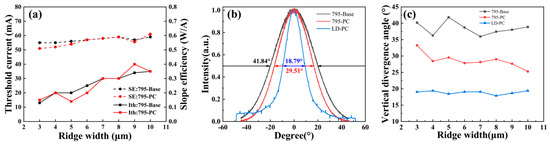
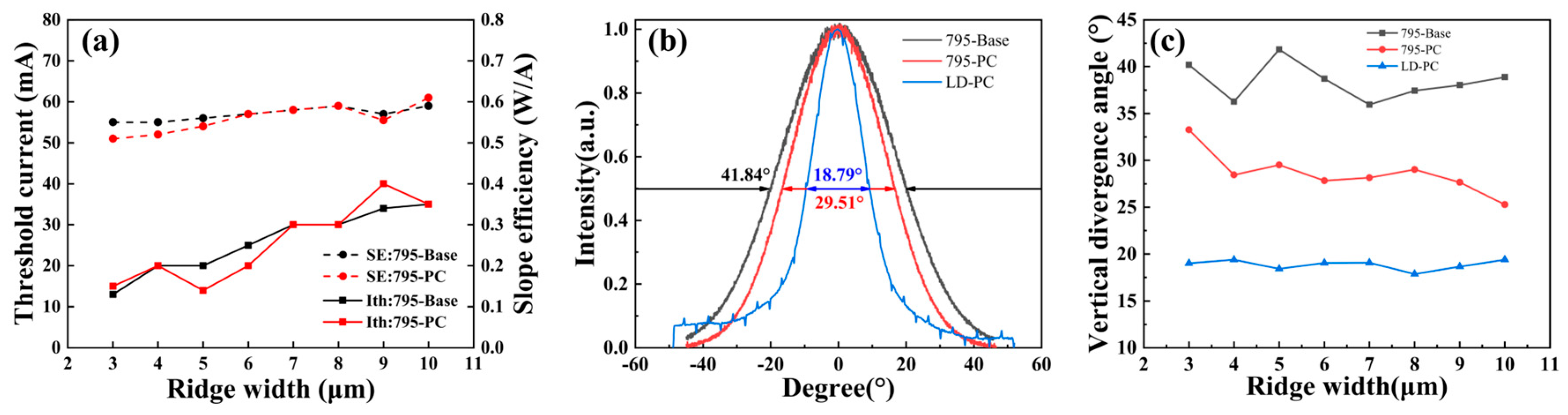
To further evaluate whether the introduction of the photonic-crystal epitaxial structure affects the basic electro-optical performance, the averaged threshold current and slope efficiency of uncoated 1 mm FP 795–Base and 795–PC lasers were compared as a function of ridge width, as shown in Figure 7a. Overall, the two structures exhibit broadly comparable performance. At ridge widths of 3, 5, and 10 μm, the averaged threshold currents are 13, 20, and 35 mA for 795–Base versus 15, 14, and 35 mA for 795–PC, while the corresponding averaged slope efficiencies are 0.55, 0.56, and 0.59 W/A versus 0.51, 0.54, and 0.61 W/A, respectively. These results indicate that, under narrow-ridge and low-current injection conditions, the introduction of the photonic-crystal layer does not cause an obvious penalty in electrical performance or electro-optical conversion efficiency.
Figure 7.
(a) Threshold current and slope efficiency of uncoated 1 mm FP 795–Base and 795–PC devices for 3–10 μm ridge width; (b) measured vertical far-field divergence profiles of the 795–Base, 795–PC, and LD–PC epitaxial structures at a ridge width of 5 μm; (c) comparison of the vertical far-field divergence angles of the 795–Base, 795–PC, and LD–PC epitaxial structures for 3–10 μm ridge width.
For the low-divergence design, the epitaxial structure without a photonic-crystal layer (795–Base) was used as the reference and compared with a structure incorporating photonic-crystal epitaxy (795–PC) and a further optimized photonic-crystal design (LD–PC) with refined composition and doping profiles. Figure 7b shows the measured vertical far-field divergence at a ridge width of 5 μm. The vertical divergence angles (FWHMs) for the 795–Base, 795–PC, and LD–PC structures are 41.84°, 29.51°, and 18.79°, respectively. In addition, for each epitaxial structure, FP laser diodes with a fixed cavity length of 1 mm and ridge widths ranging from 3 μm to 10 μm were fabricated, and the vertical far-field divergence (FWHM) was characterized. The results are summarized in Figure 7c. The 795–Base devices exhibit a vertical divergence of approximately 40°. After introducing the photonic-crystal layer, the vertical divergence of the 795–PC devices is reduced to below 30°. With further optimization of the photonic-crystal thickness, number of periods, and material composition, the LD–PC devices achieve a vertical divergence below 20°, corresponding to an overall reduction of nearly 50% compared with the reference epitaxy. Although small fluctuations are observed, the overall reduction trend remains robust, indicating that the LD–PC design preserves its divergence-suppression effect within a finite process window and therefore exhibits a certain degree of fabrication tolerance.
3.2. Performance Characterization of the LD–PC Lasers
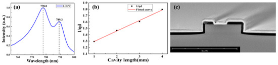
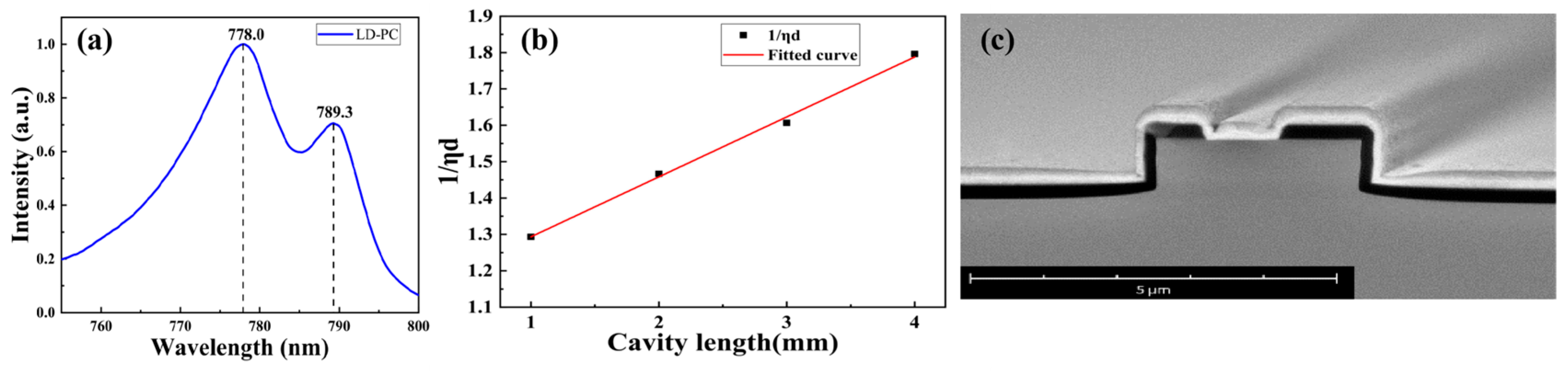
After the growth of the LD–PC structure, the photoluminescence (PL) spectrum was measured. Lasers with cavity lengths ranging from 1 mm to 4 mm were fabricated, and the internal optical loss and internal quantum efficiency were characterized using the cavity-length variation (multi-length fitting) method. For lasers with different cavity lengths, the slope efficiency is related to the internal loss and mirror loss as follows:
where is the cavity length, and and are the front- and rear-facet reflectivities, respectively (0.32 for uncoated facets).
Figure 8 presents the PL spectrum, the internal-loss fitting results, and the SEM image of the LD–PC laser diodes. The PL spectrum exhibits a double-peak feature, which can be attributed to the strain-induced splitting of the light- and heavy-hole valence bands in the tensile-strained quantum well [22,25]. In practical epitaxial tuning, the long-wavelength PL peak is generally used as the main wavelength reference because it is more relevant to the eventual lasing wavelength of the fabricated device. For the present LD–PC wafer, this long-wavelength peak is located at 789.3 nm. Using the cavity-length variation method, the LD–PC lasers were found to have an internal optical loss of 1.66 cm−1 and an internal quantum efficiency of 89%.
Figure 8.
Characterization of the LD–PC device: (a) PL spectrum; (b) internal-loss fitting results; (c) SEM image of the fabricated laser.
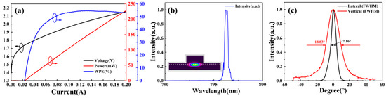
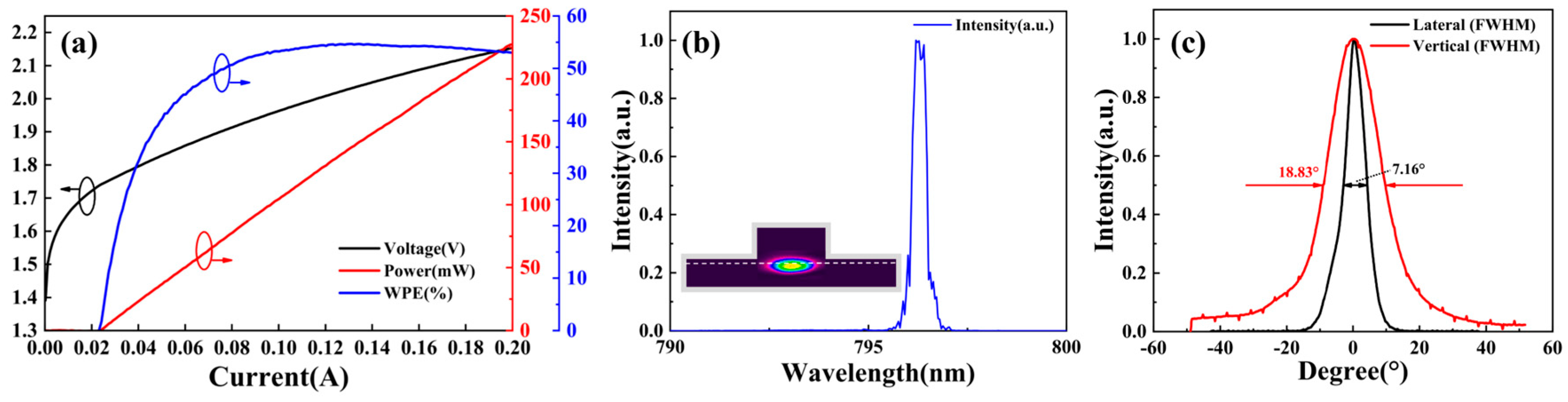
Based on the LD–PC epitaxial structure, narrow-ridge semiconductor lasers with a ridge width of 3 μm and a cavity length of 1 mm were fabricated. The rear facet was coated with a high-reflectivity (HR) film (99%), while the front facet was coated with an anti-reflection (AR) film (2%). After fabrication, the devices were characterized under CW operation at 25 °C. Figure 9a,b show the measured L–I–V characteristics and emission spectra. The device exhibits a threshold current of 23 mA and delivers an output power of 227 mW at 200 mA, corresponding to a slope efficiency of 1.28 W/A. A peak wall-plug efficiency of 55% is achieved and remains above 50% at an operating current of 200 mA. Further increasing the current to 300 mA led to a kink-like feature in the L–I curve, accompanied by the emergence of a multi-peak emission spectrum. The lasing peak wavelength is 796.8 nm. This lasing wavelength is red-shifted relative to the long-wavelength PL peak at 789.3 nm, which can be attributed to the combined effects of cavity-mode selection, carrier injection and self-heating under CW electrical operation. The measured near-field pattern shows a well-defined elliptical spot, indicating lasing in the fundamental cross-sectional mode (TM00), i.e., the coupling of the fundamental vertical and fundamental lateral modes.
Figure 9.
Performance of the LD–PC FP laser with a 3 μm ridge width and a 1 mm cavity length: (a) L–I–V characteristics; (b) emission spectra (inset: near-field intensity distribution; the white dashed line marks the active region); (c) far-field divergence characteristics.
Figure 9c shows the measured far-field divergence characteristics of the device. The FWHM divergence angles are 7.16° in the horizontal direction and 18.83° in the vertical direction. The measured vertical divergence is approximately 3° higher than the simulated value, which can be attributed to the physical factors not fully captured in the simplified model, including epitaxial-growth deviations, etch-profile non-ideality, sidewall roughness, nonuniform injection, and self-heating during CW operation. The relatively small horizontal divergence of 7.16° is associated with the selected 3 μm narrow-ridge design, which provides sufficient lateral-mode discrimination for fundamental-mode operation while still allowing the lateral optical field to extend beyond the physical ridge, thereby maintaining a comparatively large effective lateral mode size.
4. Discussion
The experimental results establish the structure-level effectiveness of the proposed photonic-crystal epitaxy. Compared with the reference 795–Base devices, the 795–PC devices show broadly comparable threshold current and slope efficiency over the investigated ridge-width range, indicating that introducing the photonic-crystal layer does not cause an obvious electro-optical penalty under the present uncoated 1 mm FP conditions. At the same time, the vertical far-field divergence is progressively reduced from the 795–Base structure to 795–PC and further to the optimized LD–PC structure. In particular, at a ridge width of 5 μm, the measured vertical divergence decreases from 41.84° to 29.51° and then to 18.79°. This value is already comparable to, or even slightly lower than, the vertical divergence reported for previously demonstrated low-divergence 780 nm photonic-crystal lasers, and is substantially smaller than the values reported for existing 795 nm narrow-ridge edge-emitting lasers [18,21]. It is also comparable to the low-divergence levels reported for photonic-crystal-based designs at longer wavelengths [9,10,11]. Moreover, the LD–PC devices maintain a vertical divergence below 20° over the tested ridge-width range, which suggests that the divergence-suppression effect is not limited to an isolated design point but can be preserved within a finite fabrication window.
From the physical perspective, the divergence reduction originates from band-edge-assisted vertical mode expansion in the PC epitaxy design, which is consistent with the general mode-expansion and modal-discrimination concepts previously explored in photonic-crystal and coupled-waveguide laser designs [9,10,11,12,13,14]. The band-structure analysis shows that the LD–PC parameters are selected such that the fundamental vertical mode is positioned close to the band edge, whereas the higher-order vertical modes remain inside the pass band. Under this condition, the fundamental mode penetrates further into the PC region, which enlarges the effective near-field size in the vertical direction and consequently narrows the far-field angular spectrum. In contrast, the higher-order modes are more likely to propagate and leak in the periodic stack, and therefore exhibit smaller confinement and reduced modal preference. The simulated near-field profile of the LD–PC structure, together with the measured reduction in vertical divergence to below 20°, is consistent with this physical picture. In addition, the parameter maps in Figure 2 indicate that the desired mode ordering is preserved within a finite range of thickness and composition, suggesting that the proposed band-edge-assisted design can tolerate moderate epitaxial deviations.
The results of LD–PC laser diodes confirm that the optimized LD–PC design provides an effective route to reducing the vertical far-field divergence of 795 nm edge-emitting semiconductor lasers while maintaining competitive electro-optical performance. For the optimized device, cavity-length analysis yields an internal optical loss of 1.66 cm−1 and an internal quantum efficiency of 89%, while the 3 μm/1 mm narrow-ridge laser delivers a threshold current of 23 mA, a slope efficiency of 1.28 W/A, and an output power of 227 mW at 200 mA under CW operation at 25 °C. Although a direct beam-quality-factor (M2) measurement was not performed in the present work, the measured near-field pattern together with the relatively small horizontal and vertical far-field divergences is consistent with lasing in the fundamental cross-sectional mode [13,24]. These results already demonstrate the feasibility of the LD–PC concept and further optimization remains possible. Under CW operation at 25 °C, the device remained operational up to 300 mA; however, kink behavior and mode hopping emerged near the upper current range, indicating the onset of thermally induced modal instability. In particular, improvements in cavity design, facet coating, and thermal management may provide additional enhancement in slope efficiency and power efficiency, while systematic studies of elevated-temperature operation and long-term reliability will be important for future application-oriented development.
5. Conclusions
A 795 nm edge-emitting laser based on photonic-crystal epitaxy was designed, fabricated, and experimentally demonstrated. The results show that the introduction of a photonic-crystal epitaxial layer can effectively suppress the vertical far-field divergence without obvious degradation of the basic electro-optical performance. Compared with the 795–Base structure, the optimized LD–PC structure achieves a much smaller vertical divergence, reaching 18.79° at a ridge width of 5 μm and remaining below 20° over the investigated ridge-width range. Based on the optimized LD–PC epitaxy, a 3 μm ridge-width, 1 mm cavity-length laser exhibits a threshold current of 23 mA, an output power of 227 mW at 200 mA, a slope efficiency of 1.28 W/A, and a peak wall-plug efficiency of 55% under CW operation at 25 °C, together with horizontal and vertical far-field divergences of 7.16° and 18.83°, respectively. These results confirm that the proposed design provides an effective route toward fabricating compact 795 nm semiconductor lasers with low vertical divergence and competitive output performance.
Author Contributions
Experiment and writing—original draft preparation, B.H.; writing—review and editing, Y.W., A.Q., Y.C., X.Z., Z.L. and W.Z. All authors have read and agreed to the published version of the manuscript.
Funding
This work was supported by National Key Research and Development Program of China (No. 2021YFA1400604).
Institutional Review Board Statement
Not applicable.
Informed Consent Statement
Not applicable.
Data Availability Statement
Data are contained within the article.
Conflicts of Interest
The authors declare no conflicts of interest.
References
- Preusser, J.; Knappe, S.; Kitching, J.; Gerginov, V. A microfabricated photonic magnetometer. In Proceedings of the 2009 IEEE International Frequency Control Symposium Joint with the 22nd European Frequency and Time Forum; IEEE: New York, NY, USA, 2009; pp. 1180–1182. [Google Scholar]
- Zhao, J.; Yang, Y.; Zhang, L.; Li, Y.; Wang, J. Improving 795 nm single-frequency laser’s frequency stability by means of the bright-state spectroscopy with rubidium vapor cell. Photonics 2024, 11, 1165. [Google Scholar] [CrossRef] [Scilit]
- Yu, N.; Blanchard, R.; Fan, J.; Capasso, F.; Edamura, T.; Yamanishi, M.; Kan, H. Small divergence edge-emitting semiconductor lasers with two-dimensional plasmonic collimators. Appl. Phys. Lett. 2008, 93, 181101. [Google Scholar]
- Yu, J.; Guo, L.; Wu, H.; Wang, Z.; Tan, H.; Gao, S.; Wu, D.; Zhang, K. High brightness beam shaping and fiber coupling of laser-diode bars. Appl. Opt. 2015, 54, 3513–3516. [Google Scholar] [CrossRef] [Scilit]
- Ning, J.; Zhang, W.; Cao, C.; Feng, Z.; Zeng, X.; Wang, T.; Wang, R.; Song, Q.; Fan, S. Collimation of laser diode beams for free space optical communications. Infrared Phys. Technol. 2019, 102, 102996. [Google Scholar] [CrossRef] [Scilit]
- Zhou, H.; Xu, H.; Duan, J. Review of the technology of a single mode fiber coupling to a laser diode. Opt. Fiber Technol. 2020, 55, 102097. [Google Scholar] [CrossRef] [Scilit]
- Zhong, S.; Xu, C.; Duan, L.; Zhang, F.; Duan, J.-A. Optimizing the efficiency of a laser diode and single-mode fiber coupling using multi-aspherical lenses. Opt. Fiber Technol. 2022, 68, 102781. [Google Scholar] [CrossRef] [Scilit]
- Zhao, S.; Qi, A.; Wang, M.; Qu, H.; Lin, Y.; Dong, F.; Zheng, W. High-power high-brightness 980 nm lasers with >50% wall-plug efficiency based on asymmetric super large optical cavity. Opt. Express 2018, 26, 3518–3526. [Google Scholar] [CrossRef] [Scilit] [PubMed]
- Chen, Z.; Qi, A.; Zhou, X.; Qu, H.; Chen, J.; Jia, Y.; Zheng, W. High power and narrow vertical divergence laser diodes with photonic crystal structure. IEEE Photonics Technol. Lett. 2021, 33, 399–402. [Google Scholar] [CrossRef] [Scilit]
- Wang, L.; Qi, A.; Zhou, X.; Fu, T.; Xu, C.; Han, R.; Qu, H.; Zheng, W. High power conversion efficiency narrow divergence angle photonic crystal laser diodes. IEEE Photonics J. 2022, 14, 1544306. [Google Scholar]
- Han, R.; Qi, A.; Fu, T.; Qu, H.; Wang, L.; Xu, C.; Zhou, X.; Zheng, W. 88× nm High-Efficiency Narrow Divergence Angle Laser Diodes with Coupled Waveguide Photonic Crystal. IEEE Photonics Technol. Lett. 2023, 35, 749–752. [Google Scholar] [CrossRef] [Scilit]
- Gordeev, N.Y.; Payusov, A.S.; Shernyakov, Y.M.; Mintairov, S.A.; Kalyuzhnyy, N.A.; Kulagina, M.M.; Maximov, M.V. Transverse single-mode edge-emitting lasers based on coupled waveguides. Opt. Lett. 2015, 40, 2150–2152. [Google Scholar] [CrossRef] [Scilit]
- Zhou, K.; Du, W.; Li, Y.; Kang, J.; Zhang, L.; Hu, Y.; Tan, H.; Wang, Z.; Gao, S.; Wu, D.; et al. Suppression of higher-order modes in a large-optical-cavity waveguide structure for high-power high-efficiency 976-nm diode lasers. Superlattices Microstruct. 2019, 129, 40–46. [Google Scholar] [CrossRef] [Scilit]
- Han, L.; Wang, Z.; Gordeev, N.Y.; Maximov, M.V.; Tang, X.; Beckman, A.A.; Kornyshov, G.O.; Payusov, A.S.; Shernyakov, Y.M.; Zhukov, A.E.; et al. Progress of edge-emitting diode lasers based on coupled-waveguide concept. Micromachines 2023, 14, 1271. [Google Scholar] [CrossRef] [Scilit]
- He, L.; Zhou, K.; Zhang, L.; Li, Y.; Du, W.; Hu, Y.; Gao, S.; Tang, C. Fabrication of high-power semiconductor laser with wavelength-locked at 780 nm. High Power Laser Part. Beams 2021, 33, 91001. [Google Scholar]
- Li, Y.; Wang, H.; Zhang, L.; He, Y.; Zhou, K.; Du, W.; He, L.; Hu, Y.; Wu, D.; Gao, S.; et al. High power semiconductor lasers with output power over 16 W for single emitter and 180 W for bar operation at 780 nm under CW operation. High Power Laser Part. Beams 2023, 35, 111002. [Google Scholar]
- Wang, B.; Zhou, L.; Tan, S.; Liu, W.; Deng, G.; Wang, J. 71% wall-plug efficiency from 780 nm-emitting laser diode with GaAsP quantum well. Opt. Laser Technol. 2024, 168, 109867. [Google Scholar] [CrossRef] [Scilit]
- Xu, C.; Qi, A.; Wang, T.; Zhou, X.; Qu, H.; Wang, L.; Wang, J.; Wang, Y.; Zheng, W. Narrow vertical divergence 780 nm lasers with modulated refractive index of photonic crystal structure. Appl. Phys. Express 2022, 15, 44002. [Google Scholar] [CrossRef] [Scilit]
- Ruan, C.; Chen, Y.; Qin, L.; Ma, D.; Jia, P.; Liu, X.; Liang, L.; Lei, Y.; Zeng, Y.; Song, Y.; et al. Purely gain-coupled distributed feedback Bragg semiconductor laser emitting at 795 nm with a wide tunable range. IEEE Photonics J. 2021, 13, 1500908. [Google Scholar] [CrossRef] [Scilit]
- Ma, D.Z.; Chen, Y.Y.; Lei, Y.X.; Jia, P.; Gao, F.; Zeng, Y.G.; Liang, L.; Song, Y.; Ruan, C.K.; Liu, X.; et al. A 795 nm gain coupled distributed feedback semiconductor laser based on tilted waveguides. Chin. Phys. B 2021, 30, 50505. [Google Scholar] [CrossRef] [Scilit]
- Qiu, P.; Zhou, H.; Wang, T.; Wang, Q.; Kan, Q. Low-threshold 795 nm oxide-confined distributed feedback lasers with surface gratings. IEEE Photonics J. 2023, 15, 1502607. [Google Scholar] [CrossRef] [Scilit]
- Pan, W.; Yaguchi, H.; Onabe, K.; Ito, R.; Shiraki, Y. Tensile-strained GaAsP/AlGaAs quantum wells grown by low-pressure metalorganic vapor phase epitaxy. J. Appl. Phys. 1995, 78, 3517–3519. [Google Scholar] [CrossRef] [Scilit]
- Mawst, L.J.; Kim, H.; Smith, G.; Sun, W.; Tansu, N. Strained−layer quantum well materials grown by MOCVD for diode laser application. Prog. Quantum Electron. 2021, 75, 100303. [Google Scholar] [CrossRef] [Scilit]
- Miah, M.J.; Strohmaier, S.; Urban, G.; Bimberg, D. Beam quality improvement of high-power semiconductor lasers using laterally inhomogeneous waveguides. Appl. Phys. Lett. 2018, 113, 221107. [Google Scholar] [CrossRef] [Scilit]
- Wang, B.; Zeng, Y.; Yu, X.; Gao, W.; Chen, W.; Shen, H.; Qin, L.; Ning, Y.; Wang, L. Impact of the Interruption Duration on Photoluminescence Properties of MOCVD-Grown GaAsP/InAlGaAs Quantum Well Structures. Nanomaterials 2024, 14, 1469. [Google Scholar] [CrossRef] [Scilit] [PubMed]
Disclaimer/Publisher’s Note: The statements, opinions and data contained in all publications are solely those of the individual author(s) and contributor(s) and not of MDPI and/or the editor(s). MDPI and/or the editor(s) disclaim responsibility for any injury to people or property resulting from any ideas, methods, instructions or products referred to in the content. |
© 2026 by the authors. Licensee MDPI, Basel, Switzerland. This article is an open access article distributed under the terms and conditions of the Creative Commons Attribution (CC BY) license.