Article

Broadband Absorption in Mid-Infrared via Trapezoidal Gratings Made of Anisotropic Metamaterial

1
College of Electronic and Optical Engineering & College of Flexible Electronics (Future Technology), Nanjing University of Posts and Telecommunications, Nanjing 210023, China
2
National Laboratory of Solid-State Microstructures, College of Engineering and Applied Sciences, Nanjing University, Nanjing 210093, China
3
State Key Laboratory of Millimeter Waves, Southeast University, Nanjing 210096, China
*
Authors to whom correspondence should be addressed.
Photonics 2025, 12(9), 932; https://doi.org/10.3390/photonics12090932
Submission received: 18 August 2025 / Revised: 16 September 2025 / Accepted: 17 September 2025 / Published: 18 September 2025
(This article belongs to the Special Issue Recent Progress in Optical Metamaterials and Metasurfaces)

Abstract

Broadband absorption of electromagnetic energy plays an important role in energy harvesting and stealth. Here, we present and demonstrate an absorber with a wide bandwidth of 2.1 μm in mid-infrared. The trapezoidal metamaterial consists of alternating silicon carbide and dielectric films. We have numerically demonstrated that an ultrahigh absorption energy efficiency higher than 97.7% can be calculated from 10.6 μm to 12.7 μm. The proposed absorber has high absorption efficiency at a wide-angle range. The simulation results are consistent with the theoretical calculation based on effective medium theory. The theoretical model simplifies the multilayer structure into an effectively homogeneous metamaterial with hyperbolic dispersion. In addition, the distributions of magnetic field depict that different wavelengths can be trapped at structures with various widths. The mechanism of this phenomenon is attributed to the slowlight modes. Furthermore, a dual-sized absorber is designed to achieve high efficiency and broadband absorption, which is easy to manufacture. Our study has potential applications in the areas of energy harvesting materials, thermal emitters and photovoltaic devices in the mid-infrared.

1. Introduction

Numerous studies have focused on metamaterials (MMs) due to its exhibit many distinctive phenomena that do not exist in nature [1,2,3,4,5,6,7,8,9], such as negative refraction [4], perfect lens [5], cloaking [6], absorbers [7,8,9], etc. In most applications, the absorption loss will be the critical parameters to evaluate the performance of MMs; but on the other word, the absorption loss becomes useful in many applications. For instance, metamaterial absorbers (MAs) have become a crucial component of thermal emitters [10,11] and detectors [12]. Meanwhile, broadband MAs are of increasing importance in many applications, such as energy harvesting materials [13] and photovoltaic devices [14]. In 2008, Landy et al. first proposed that perfect absorption of metamaterials can be achieved at a specific wavelength [7]. After this, some improvement works have been investigated in a wide spectral regime ranging from microwave to terahertz and visible light [13,14,15,16,17,18,19]. However, many MAs generally exhibit narrowband absorption, which limits its optical properties on broadband light absorption and emission. To further broaden the absorption bandwidth, the slowlight effect of MAs consisting of multilayered metallic-dielectric can achieve a large bandwidth [20,21,22,23]. The slowlight modes confines energy within hyperbolic metamaterial, enabling high absorption of incident light. In particular, the slowlight waveguide is straightforward. By etching, the multilayer structure can be transformed into a graded profile, the thickness of each layer gradually varies from top to bottom.
Recently, optical absorber operating in the mid-infrared (MIR) band is of considerable interest for sensing, detecting, radiation and so on. With many designs formed by alternately stacking metal sheets and dielectric plates, the absorber can be operated in this waveband [24,25,26,27,28]. However, due to the disadvantages of metal materials that are easily corroded and susceptible to high temperature, we have to find alternative materials. Fortunately, silicon carbide (SiC) is an ideal substitute for metal because it can exhibit metallic properties in MIR, and it has unique characteristics, such as good thermal resistance, good chemical inertness and low thermal expansion [29,30], etc. Furthermore, as a kind of the important compound semiconductors, numerous studies have focused on SiC-based nanostructures [31,32].
In this paper, we design a trapezoidal MA composed of alternating SiC and dielectric films, achieving broad spectrum absorption in MIR. We numerically investigate the absorption performance of the proposed MA across the 10.6–12.7 μm wavelength range. The numerical results show that the absorptivity of higher than 97% can be achieved. The proposed absorber maintains consistently high absorption efficiency across a wide 75° angular range. Moreover, the absorption spectrum calculated by the effective medium theory (EMT) is similar to that of the actual model. The magnetic field distribution plots reveal a progressive downward shift in field energy concentration from the upper to lower structural layers as wavelength increases, indicating wavelength-dependent absorption localization within the absorber. Combined with theoretical and numerical results, we can conclude that this is a typical slowlight effect. Furthermore, a dual-sized MA is designed to realize high efficiency and broadband absorption. Unlike the MA based on metal, our design opens a new avenue towards realizing energy harvesting materials, thermal emitters and photovoltaic devices in the mid-infrared.

2. Materials and Methods

Figure 1 illustrates the schematic of the proposed broadband MA and geometric parameters of the unit cell. In detail, the MA consists of an array of multilayered SiC/dielectric trapezoidal structure with thick enough silver film placed under the structure to inhibit transmission. The dielectric layer is assumed to be the polymer with a permittivity of εd = 2.1 which exhibits negligible optical loss. The period of each unit cell is P = 3 μm. The top and bottom width of proposed trapezoidal structure is Wt = 0.1 μm and Wb = 2.7 μm, respectively. The thickness of SiC and dielectric layer is ts = 0.2 μm and td = 0.2 μm, respectively. The number of SiC and dielectric pairs is denoted by N. The incident light is TM-polarized plane wave (magnetic field is parallel to y-axis) with an incident angle θ. The operating wavelength in this paper ranges from 10.6 μm to 12.7 μm.
The permittivity of silver can be described by the Drude model [33]:
ε s i l v e r = ε ω p 2 ω 2 + i γ ω
where ω is the operating frequency, plasma frequency ωp = 1.39 × 10¹⁶ rad/s, scattering rate γ = 2.7 × 10¹³ rad/s, and ε = 3.4.
The permittivity of SiC was computed from Ref. [29]:
ε S = ε ω 2 ω L O 2 + i Γ ω ω 2 ω T O 2 + i Γ ω
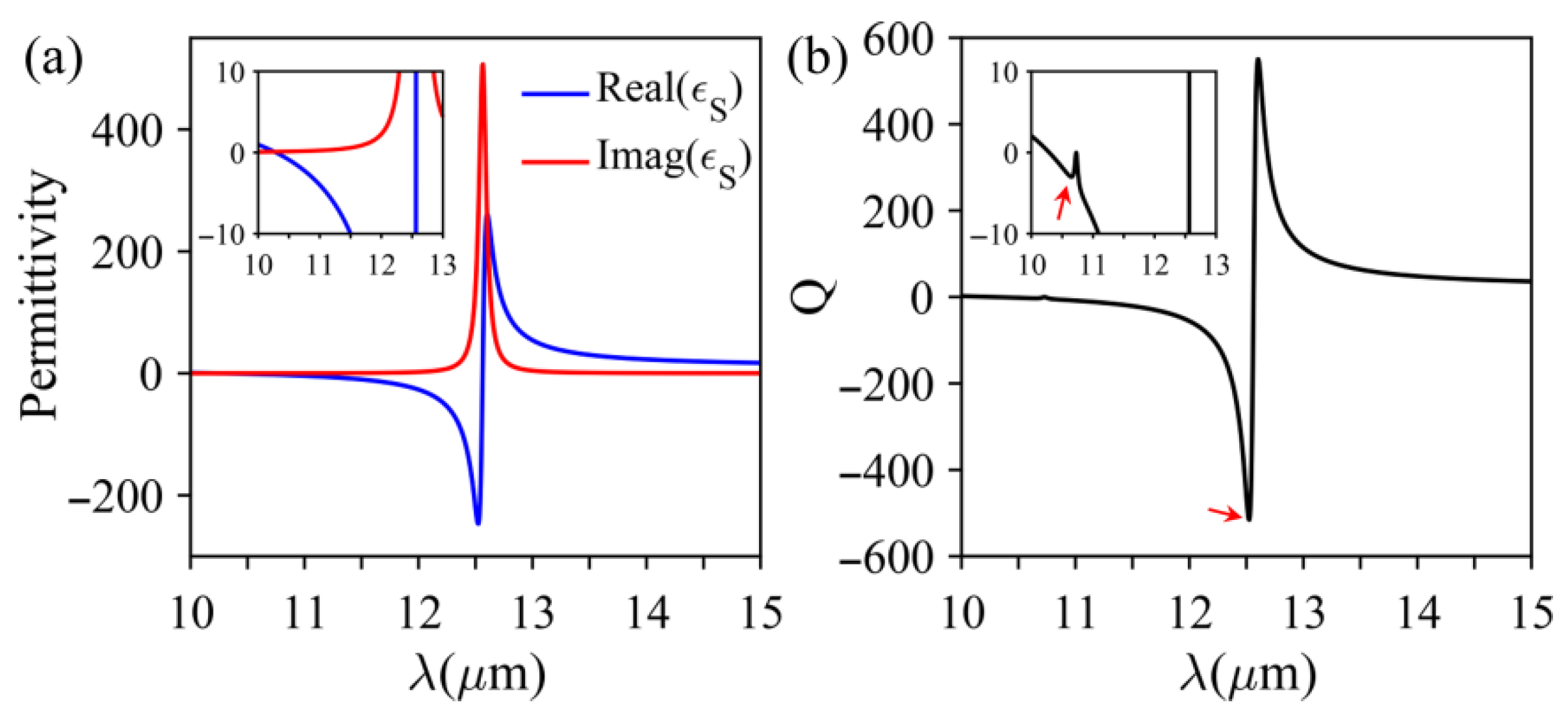
Here, ωLO = 972 cm−1, ωTO = 796 cm−1, ε = 6.5 and Γ = 5 cm−1. The permittivity of SiC is shown in Figure 2a. In the wavelength range from 10.29 μm to 12.56 μm, the SiC material exhibits metallic properties due to its real part of permittivity is less than zero.
According to EMT [34], when the structural thickness of SiC and polymer layer (ts = td = 0.2 μm) is much smaller than the incident wavelength (10.6 μm < λ < 12.7 μm), the proposed multilayer structure can be equivalently modeled as homogeneous medium with effective anisotropic permittivity. The permittivity tensor of the effective medium can be written as [34]:
ε x = ε y = f ε S + 1 f ε d ε z = ε S ε d f ε d + 1 f ε S
where f = ts/(ts + td) is the filling ratio of the SiC. When Q (Q = Re(εx)·Re(εz)) < 0, the iso-frequency surface is hyperboloid; however, it turns into ellipsoidal, while Q > 0. The value of Q is shown in Figure 2b. In the wavelength range of 10.3 μm to 12.56 μm, the multilayer structure has the characteristic of hyperbolic dispersion, but two mutation points occur near the 10.6 μm and 12.52 μm (as shown by red arrows in Figure 2b), which may greatly affect the performance of the MA.
The bottom silver film is thick enough to suppress all transmission, so the absorption can be defined by A = 1 − |S11|2 − |S21|2 with |S21| = 0, where S11 and S21 are S-parameters relevant to reflection and transmission coefficient, respectively. From the perspective of impedance matching, the effective impedance of MA can be written as [35,36]
Z = 1 + S 11 2 S 21 2 1 S 11 2 S 21 2
When the effective impedance of MA matches that of free space (Z = Z0 = 1), the reflection will be effectively suppressed and high absorptivity can be achieved.
In addition, the total energy absorption efficiency (α) can be used to evaluate the performance of the absorber, and α is the integral of the total incident energy absorbed on the considered wave band:
α = λ 1 λ 2 A λ d λ λ 2 λ 1
where λ1 and λ2 correspond to the start and end of the wavelength range, respectively. Here, λ1 and λ2 are determined by the full width at half maximum (FWHM). In general, the larger the total absorption energy efficiency, the better the performance of the absorber at the regarded wave band.

3. Results

3.1. Broadband Absorption Efficiency Based on Multilayer Structure

Under a normal incident of TM-polarized plane wave, the absorption spectrum is obtained by finite element method (FEM), as shown by the blue solid curve in Figure 3a. In the simulation, we employed a two-dimensional structural model using customized mesh elements, included the maximum element size is 40 nm, total mesh vertices are 22,156, triangular elements are 43,674, edge elements are 2409, and endpoint elements are 95. Periodic boundary conditions are applied along the x axis, and perfectly matched layers are implemented for the z axis. The absorption spectrum shows an absorption efficiency of over 90% in the wavelength range of 10.64 μm to 12.64 μm, especially nearly perfect absorption (more than 97%) occurs from 10.67 μm to 12.47 μm. The total absorption energy efficiency higher than 97.7% can be calculated over the operational wave band, which indicates that most of the incident energy is absorbed by the structure. In addition, we can also observe that there are two dips near 10.6 μm and 12.52 μm (as shown by the blue arrows in the left inset of Figure 3a), which is due to the obvious mutation of the value of Q, corresponding to Figure 2b. The FWHM is 2.4 μm which obtained from 10.33 μm to 12.73 μm. The wide absorbing bands is much larger than that reported in Ref. [37].
In order to verify the results of the multilayer structure, we compared it with EMT. The equivalent trapezoidal structure consists of a homogeneous, anisotropic material, as shown in the right inset of Figure 3a. Obviously, the absorption efficiency acquired from equivalent trapezoidal structure (red solid curve in Figure 3a) is similar to the actual model. The similarity of the two curves directly indicates that the EMT is applicable in our model. Moreover, in the wavelength range from 10.64 μm to 12.64 μm, the real part of the MA’s effective impedance Re(Z) fluctuates in the small range near 1 and its imaginary part Im(Z) fluctuates in the small range near 0, as shown in Figure 3b. Therefore, the MA’s effective impedance is basically equal to the free space impedance (Z = Z0 = 1). This greatly suppresses the reflection of the incident wave by the MA, thereby achieving high absorption. For broadband absorbers, angular tolerance is a crucial performance metric and holds significant importance for practical applications. Therefore, the simulated and theoretical absorption spectra as a function of incident angles are depicted in Figure 3c,d. These results indicate that the broadband absorption efficiency is insensitive to the incident angle. In the wavelength range of 10.64 μm to 12.64 μm, the absorptivity is higher than 90% even when the incident angle reaches 75°. Moreover, the simulation results agreed well with the theoretical results.

3.2. Principle of the Broadband Absorption Based on Multilayer Structure

The principle of broadband absorption can be understood from the following two aspects:
(i) On the one hand, to better understand the process of incident light absorption, the normalized magnetic field distributions (|Hy|) at different incident wavelengths (λ = 11.2 μm, 11.6 μm, 12 μm and 12.4 μm) of multilayer structure and equivalent trapezoidal structure are shown in Figure 4. The electromagnetic field appears to be localized and effectively confined within varying widths of the trapezoidal metamaterial absorber at different wavelengths. Obviously, at a smaller wavelength, the electromagnetic field is localized at the top of MA, and the electromagnetic field gradually moves toward the bottom of the MA as the wavelength increases. For instance, for λ = 11.2 μm, the magnetic field is mainly trapped at the upper region of the MA (W = 1.0 μm); for λ = 12.0 μm, the magnetic field is localized at the middle region (W = 1.9 μm); and for λ = 12.4 μm, the magnetic field is mainly trapped at the bottom region. Particularly, unlike the magnetic response [38], the magnetic field does not remain localized within the dielectric layer between adjacent SiC layers, but rather exhibits a distributed penetration across multiple layers. This indicates that the electromagnetic wave accumulates at a certain width of the MA and is finally absorbed. In addition, we can clearly see from the bottom row of Figure 4 that the distributions of magnetic field calculated by the EMT are very similar to the actual MA. Such a good agreement among these magnetic field distributions illustrates that the EMT used here is valid. Moreover, the energy flow diagram shown by the black arrows in Figure 4 implies a noticeable light trapping effect. According to the aforementioned analyses, the electromagnetic waves of different wavelengths are trapped in different parts of the absorber, resulting in broadband spectrum absorption. These phenomena are typical characteristics of the slowlight effect.
(ii) On the other hand, to further demonstrate the slowlight effect, we calculated the dispersion curves of a periodic hyperbolic waveguide array with different fixed core widths. The dispersion relationship between the incident wave vector (k0) and the propagation constant (β) can be expressed as [39]
exp i k 2 W + k 1 i k 2 ε z k 1 + i k 2 ε z = 0
where k1 = (β2 −  k 0 2 )1/2, k2 = [εz k 0 2  − (εzx)β2]1/2, and W is the core width. Dispersion curves of fundamental mode at W = 1.0 μm, 1.4 μm, 1.9 μm and 2.1 μm are shown in Figure 5a. For a slowlight mode, the electromagnetic propagating wave experiences significant deceleration and becomes effectively trapped within the engineered hyperbolic MA. This trapping phenomenon occurs as the wave propagates progressively along the waveguide structure until reaching a critical core width where the group velocity (vg = dk0/) is close to zero.
Additionally, we observe that for small incident wave vectors (k0 < 0.49 × 10⁶ rad/m), the propagation constant exhibits a linear relationship with k0, where the slope closely matches that of light propagating in vacuum. As the wave vector approaches the cutoff condition, the dispersion curve demonstrates a slight nonlinear increase. Beyond this cutoff point, the dispersion relation flattens significantly. Figure 5b reveals a critical transition point in the dispersion characteristics when the propagating mode nears the cutoff wave vector, corresponding to the condition where the group velocity vanishes (vg = 0). This demonstrates that in a hyperbolic metamaterial waveguide with precisely engineered core dimensions, the slowlight mode can be selectively excited within specific wavelength ranges adjacent to this critical transition point. In addition, as the W increases, the cutoff wave vector also decreases, and the corresponding resonant wavelength increases, which is consistent with the phenomenon in Figure 4. Theoretically, for W = 1 μm, we can acquire that when the group velocity equals zero, the corresponding β, k0 and λ0 are 7.92 × 10⁵ rad/m, 5.62 × 10⁵ rad/m and 11.18 μm, respectively. For W = 1.9 μm, the corresponding β, k0 and λ0 are 9.77 × 10⁵ rad/m, 5.27 × 10⁵ rad/m and 11.92 μm, respectively. The simulated results are in good agreement with the EMT, which indicates that the broadband absorption arises from the slowlight effect.

3.3. Effects of the Structure Geometry

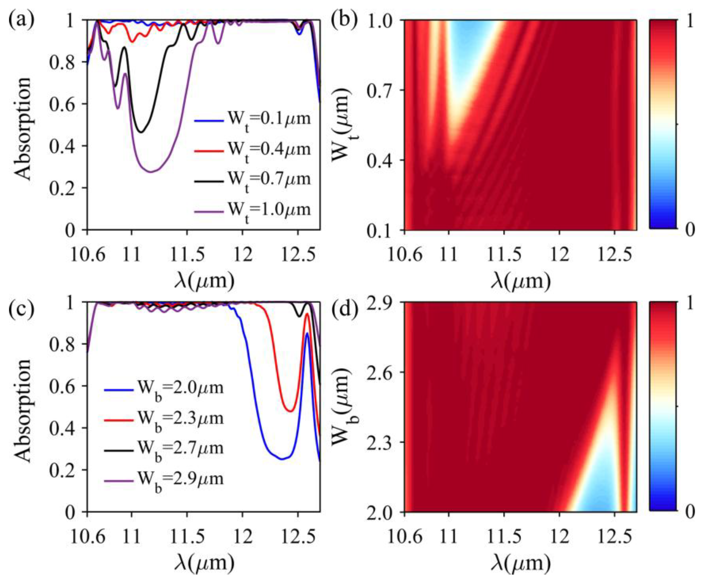
Next, we investigate the influence of different geometric parameters of the structure on the absorption efficiency. It should be noted that each parameter, such as the top width (Wt), the bottom width (Wb) and the total number of SiC/dielectric pairs (N), varies separately, while leaving other parameters unchanged. As shown in Figure 6a,b, it can be clearly seen that a larger Wt results in a decrease in absorptivity. The relationship implies that increasing Wt compromises absorption efficiency at shorter wavelengths. Notably, absorptivity remains relatively stable (0.1–0.4 μm top width range), but experiences significant attenuation at shorter wavelengths when the top width exceeds this optimal range. Similarly, as the bottom width gradually increases, it can absorb larger incident waves, as shown in Figure 6c,d. The increase in Wt from 2.6 μm to 2.9 μm has little influence on the absorptivity, but with the decrease in the bottom width, the corresponding absorption of the larger wavelengths will also be greatly weakened. This phenomenon can be attributed to the slowlight effect, where the electromagnetic field demonstrates wavelength-selective localization within the absorber. Notably, the resonant modes exhibit a strong dependence on the structural width, suggesting a direct correlation between waveguide geometry and optical confinement.
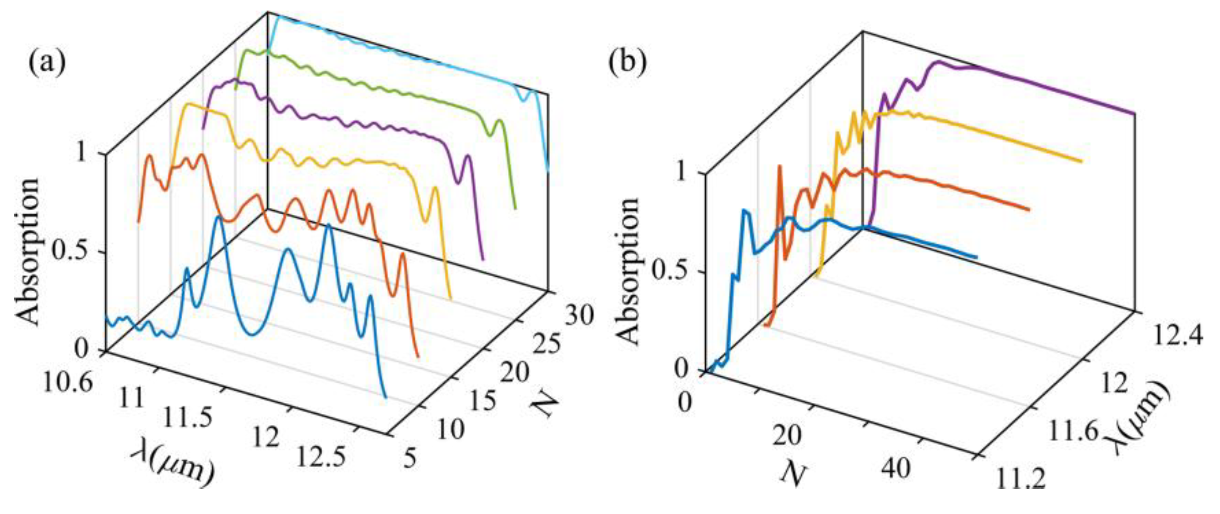
The effect of the number of composite layers on the absorptance of structure is shown in Figure 7. When keeping other parameters unchanged, the number of SiC/dielectric pairs (N) is increased from 5 to 30, and the corresponding absorption spectra are shown in Figure 7a. Obviously, as the number of composite layers increases, the absorption spectrum becomes more and more stable. In detail, for N = 5, with increasing wavelength, the main absorption layer shifts downward. The reason can be explained by the relationship between the group velocity and propagation constant. When the incident wave vector is small (k0 < 0.49 × 10⁶ rad/m), the propagation constant increases linearly with the incident wave vector, and the slope is close to the slope of the light in the vacuum; then, the incident electromagnetic wave approaches the cutoff wave vector and the dispersion line increases slightly; after the cutoff wave vector, the dispersion line becomes flat, as shown in Figure 5. This indicates that there exists absorption difference at different wavelengths, and the perfect absorption efficiency can be obtained at the cutoff wave vector. When N = 15, the absorptivity can be maintained above 75% in the wavelength range 10.63 μm to 12.63 μm. However, for N < 15, the absorptivity of the entire absorption band will be significantly weakened. Moreover, the calculated total energy absorption efficiency in the wavelength ranges from 10.6 μm to 12.7 μm is 46.9% (N = 5), 77.5% (N = 10), 90.3% (N = 15), 93.4% (N = 20), 96.4% (N = 25), and 97.7% (N = 30), respectively. The numerical results show that the absorption effect is positively correlated with the N. In addition, we select several wavelengths and study the effect of N on the absorption spectrum by gradually increasing N, as shown in Figure 7b. The absorptivity tends to stabilize around 100% when N > 20. In addition, the overall absorption efficiency of the structure demonstrates increasingly closer alignment with the theoretical values predicted by the EMT model (Figure 3) as the layer number increases. This improved agreement primarily stems from the enhanced consistency between the multilayer configuration and the theoretical framework, thereby enabling superior absorption performance.
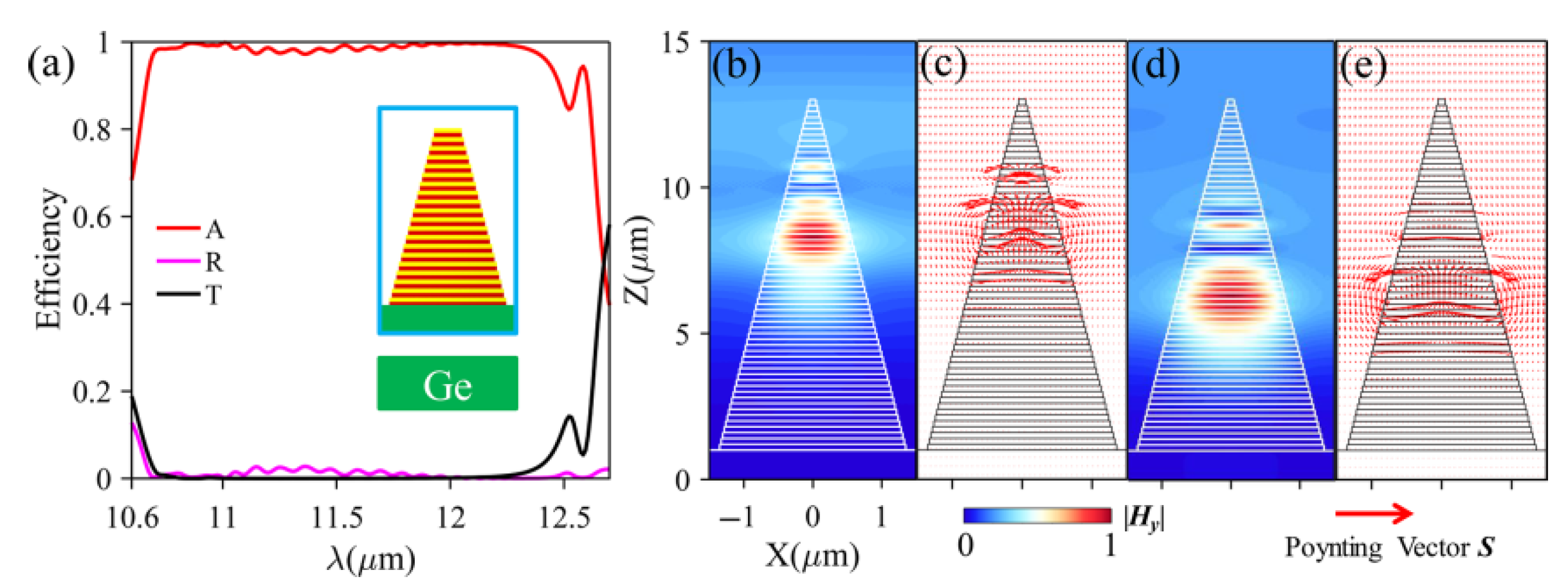
To further characterize the absorber’s performance, we investigate the substrate’s influence on the spectral absorption characteristics. As mentioned in Ref. [39], the metal substrate plays an important role in enhancing absorption. However, in our design, the metal substrate has little effect on the absorption spectrum, as shown in Figure 8a. We have studied a modified structure by removing the silver substrate, i.e., placing the trapezoidal grating structure directly on the germanium (Ge, refractive index nGe = 4) substrate, as shown in the inset of Figure 8a. By comparing Figure 8a with Figure 3a, the absorption spectrum exhibits remarkable stability, with negligible variation, except for a slight decrease in the absorptivity around 10.6 μm and 12.5 μm. This is because the dielectric substrate cannot completely block transmission as the silver substrate, so transmission still exists in the studied band (depicted in Figure 8a by the black line). Moreover, the transmission of the absorber is almost zero in the wavelength range from 10.7 μm to 12.3 μm, which means that the substrate has no effect in this band, and the incident energy is completely absorbed before it reaches the bottom of the absorber. The total absorption energy efficiency higher than 95.7% can be calculated at the regarded wave band. We present the distributions of magnetic field and the energy flow maps of 11.6 µm and 12.0 μm, from which it can be observed that there is almost no energy in the output region of the Ge substrate, as shown in Figure 8b–e.

3.4. Broadband Metamaterial Absorber Based on Dual-Sized Trapezoidal Gratings

According to the aforementioned analyses, the larger N, the better the performance of the metamaterial absorber, but the manufacturing difficulty and the manufacturing cost are also increased. To enhance the absorber’s performance without increasing N, we designed a dual-sized trapezoidal MA. The top and bottom widths of the small trapezoidal absorber are Wa = 0.1 μm and Wc = 2.7 μm, respectively, and Wb = 0.2 μm and Wd = 2.8 μm for the large trapezoidal strip. The high absorptivity (more than 97%) in the wavelength ranges from 10.69 μm and 12.59 μm can be obtained except that a concave peak with an absorption efficiency of 82.7% appears at 12.51 μm, and the total absorption energy efficiency can reach as high as 95.9%, which is larger than what is reported in many works. These results show that high-efficiency broadband absorption can also be achieved through this dual-sized trapezoidal gratings, and its performance is comparable to that of single-sized MA with 30 SiC/dielectric pairs.
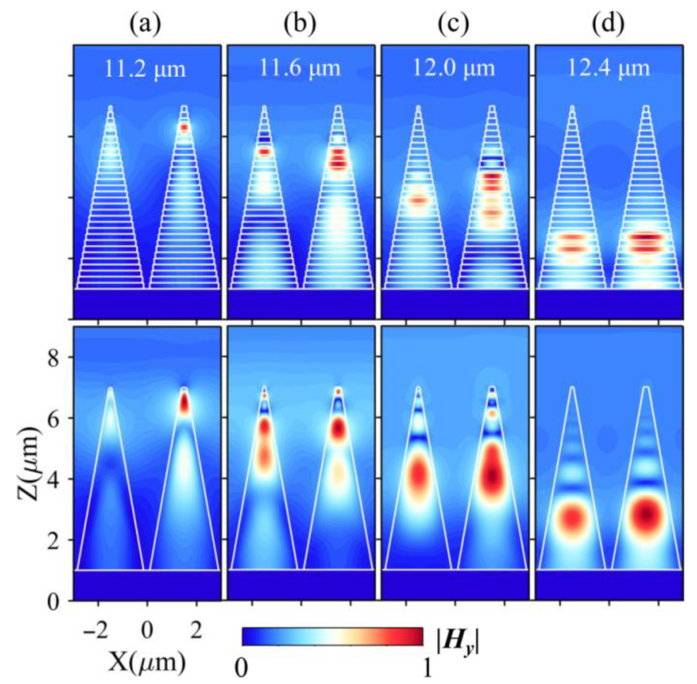
Intuitively, the absorber has small N, which means that the gradient of the width is large. According to Equation (6), for a specific incident wavelength, there may be no appropriate width to satisfy the equation. On the contrary, the absorber with large N has more optional width, and more easily match Equation (6). Moreover, the magnetic field distributions of the dual-sized MA and that of the corresponding effective homogeneous model were observed at four different wavelengths (λ = 11.2 μm, 11.6 μm, 12 μm and 12.4 μm), as shown in Figure 9. Evidently, the difference in the mode field distributions between the small and large trapezoidal gratings is due to the difference in the size of the two trapezoidal gratings in one period. Moreover, the larger trapezoidal structure on the right supports more resonant modes, leading to a stronger local field enhancement compared to the left side. To be specific, for λ = 11.2 µm, the large trapezoidal grating plays a major role in light absorption, and almost all incident energy is captured and absorbed in it. When the wavelength gets larger (λ > 11.2 µm), the small one also absorbs the incident light, which means both the small and large trapezoidal gratings contribute to the absorption. As we mentioned above, when the width increases from top to bottom, a longer wavelength is harvested at a wider width. In addition, electromagnetic field is accommodated at multiple regions within both the small and large trapezoidal gratings. The field distributions calculated by EMT are similar with that of practical model, except for some details around SiC/dielectric interfaces due to the average effect of EMT. This phenomenon demonstrates that distinct electromagnetic wavelengths are effectively confined within varying spatial regions of the absorber, facilitating broadband spectral absorption. Such wavelength-dependent localization behavior represents characteristic manifestations of the slowlight effect in photonic structures, which is consistent with the results previously shown in Figure 4.
Finally, we further investigate the dependence of the absorptivity on the number of SiC/dielectric pairs (N) and incident angle. As can be seen from Figure 10a, as N increases, the performance of the absorber is improving. This trend is similar to Figure 7. We calculate that when N = 5, 10, 15, 20, 25 and 30, the corresponding total energy absorption efficiency is 53.3%, 86.0%, 95.9%, 96.3%, 97.0% and 98.0%, respectively. It can be found that in the case of the same number of SiC/dielectric pairs, the dual-sized absorber has better performance than that of the single-sized absorber. Therefore, this dual-sized design can be used to save costs and reduce steps in the fabrication procedures. In addition, the simulated absorption spectra at different incident angles are plotted in Figure 10b. The broadband absorption exhibits remarkable angular stability, maintaining an absorptivity exceeding 85% across 10.71–12.38 μm even at a 60° incidence angle.

4. Discussion

A mid-infrared broadband trapezoidal MA has been proposed to achieve ultrahigh absorptivity from 10.6 μm to 12.7 μm over a wide incident angle. The ultrahigh total absorption energy efficiency (97.7%) can be obtained at the regarded wave band. Compared with other metal-based MAs, our designed SiC-based MA has better stability due to the unique characteristics of SiC. In addition, we systematically evaluated the absorption performance of the MA through both theoretical analysis and numerical simulations. The observed broadband absorption can be primarily attributed to the slowlight effect, which significantly enhances light–matter interaction within the structure. The effects of the structural parameters are investigated. Considering the difficulty and cost of manufacturing, we have designed a dual-sized MA that also achieves high efficiency and broadband absorption with few layers. This work holds significant potential for applications in the field of energy harvesting materials, thermal emitters, and photovoltaic devices.

Author Contributions

Conceptualization, Y.R. and Y.Q.; methodology, Y.R. and Y.Q.; software, Y.R. and Y.Q.; validation, Y.R. and Y.Q.; formal analysis, Y.R. and Y.Q.; investigation, Y.R. and Y.Q.; resources, Y.R. and Y.Q.; data curation, Y.R. and Y.Q.; writing—original draft preparation, Y.R.; writing—review and editing, Y.R., J.G., Z.J., Z.Y., J.L., Y.G. and Y.Q.; visualization, Y.R. and Y.Q.; supervision, Y.Q.; project administration, Y.G. and Y.Q.; funding acquisition, Y.G. and Y.Q. All authors have read and agreed to the published version of the manuscript.

Funding

This research was funded by the National Natural Science Foundation of China (No. 62305173), the Open Project of the State Key Laboratory of Millimeter Waves (No. K202433, No. KN202502-12), the Natural Science Foundation of the Jiangsu Higher Education Institutions of China (No. 23KJB140015), the Youth Talent Support Program of the Jiangsu Association for Science and Technology (No. JSTJ-2024-390), the China Scholarship Council (No. 202408320327), and Natural Science Research Start-up Foundation of Recruiting Talents of Nanjing University of Posts and Telecommunications (No. NY222080, No. NY225050).

Institutional Review Board Statement

Not applicable.

Informed Consent Statement

Not applicable.

Data Availability Statement

The original contributions presented in this study are included in the article. Further inquiries can be directed to the corresponding author.

Conflicts of Interest

The authors declare no conflicts of interest.

Abbreviations

The following abbreviations are used in this manuscript:
MMsMetamaterials
MAsMetamaterial absorbers
MIRMid-infrared
SiCSilicon carbide
EMTEffective medium theory
FEMFinite element method
FWHMFull bandwidth at half-maximum
GeGermanium

References

  1. Cui, T.J.; Smith, D.R.; Liu, R. Metamaterials, Theory, Design, and Applications, 1st ed.; Springer: New York, NY, USA, 2010; pp. 49–58. [Google Scholar]
  2. Zheludev, N.; Kivshar, Y. From metamaterials to metadevices. Nat. Mater. 2012, 11, 917–924. [Google Scholar] [CrossRef] [PubMed]
  3. Venturi, G.; Mancini, A.; Melchioni, N.; Chiodini, S.; Ambrosio, A. Visible-frequency hyperbolic plasmon polaritons in a natural van der Waals crystals. Nat. Commun. 2024, 15, 9727. [Google Scholar] [CrossRef]
  4. Shelby, R.A.; Smith, D.R.; Schultz, S. Experimental verification of a negative index of refraction. Science 2001, 292, 77–79. [Google Scholar] [CrossRef] [PubMed]
  5. Pendry, J.B. Negative refraction makes a perfect lens. Phys. Rev. Lett. 2000, 85, 3966–3969. [Google Scholar] [CrossRef]
  6. Ma, H.; Cui, T.J. Three-dimensional broadband ground-plane cloak made of metamaterials. Nat. Commun. 2010, 1, 21. [Google Scholar] [CrossRef]
  7. Landy, N.I.; Sajuyigbe, S.; Mock, J.J.; Smith, D.R.; Padilla, W.J. Perfect metamaterial absorber. Phys. Rev. Lett. 2008, 100, 207402. [Google Scholar] [PubMed]
  8. Ren, Z.; Yang, Z.; Mu, W.; Liu, T.; Liu, X.; Wang, Q. Ultra-broadband perfect absorbers based on biomimetic metamaterials with dual coupling gradient resonators. Adv. Mater. 2025, 37, 2416314. [Google Scholar] [CrossRef]
  9. Estevez, D.; Qin, F. High-performance carbonaceous absorbers: From heterogeneous absorbers to data-driven metamaterials. Carbon 2025, 233, 119850. [Google Scholar] [CrossRef]
  10. Qing, Y.M.; Liu, J.; Yang, Z.; Gou, Y.; Wu, L.; Wu, J. Dynamic modulation of dual-band nonreciprocal radiation in a graphene-Weyl semimetal plasmonic structure. Appl. Phys. Lett. 2025, 126, 162203. [Google Scholar] [CrossRef]
  11. Qing, Y.M.; Liu, J.; Yang, Z.; Wu, L.; Gou, Y.; Wu, J.; Li, B. Dynamic modulation of nonreciprocal absorption in a graphene–InAs hybrid structure under low magnetic field and small incident angles. Opt. Lett. 2025, 50, 1552–1555. [Google Scholar] [CrossRef]
  12. Xiong, H.; Deng, J.; Yang, Q.; Wang, B.; Wang, X.; Zhang, H. A metamaterial energy power detector based on electromagnetic energy harvesting technology. ACS Appl. Electron. Mater. 2024, 6, 1204–1210. [Google Scholar] [CrossRef]
  13. Qing, Y.M.; Wang, H.; Lei, D. Wide-angle ultrabroadband absorption in black phosphorus/dielectric multilayer anisotropic metamaterials. J. Opt. 2024, 26, 065101. [Google Scholar] [CrossRef]
  14. Yun, M.J.; Sim, Y.H.; Lee, D.Y.; Cha, S.I. Honeycomb-structured 3D concave photovoltaic modules supported by 3D mechanical metamaterials for enhance light recapture. Adv. Mater. Technol. 2023, 8, 2201360. [Google Scholar] [CrossRef]
  15. Qing, Y.M.; Ma, H.; Cui, T. Tailoring anisotropic perfect absorption in monolayer black phosphorus by critical coupling at terahertz frequencies. Opt. Express 2019, 26, 32442–32450. [Google Scholar] [CrossRef]
  16. Wang, Y.; Liu, Z.; Zhou, F.; Yi, Z.; Wang, J. Perfect absorption properties of a near-infrared super-surface perfect absorber based on a multilayer subwavelength array structure. Phys. Lett. A 2025, 540, 130395. [Google Scholar] [CrossRef]
  17. Song, M.; Feng, L.; Huo, P.; Liu, M.; Huang, C.; Yan, F.; Lu, Y.; Xu, T. Versatile full-colour nanopainting enabled by a pixelated plasmonic metasurface. Nat. Nanotechnol. 2023, 18, 71–78. [Google Scholar] [CrossRef] [PubMed]
  18. Xiao, S.; Liu, T.; Cheng, L.; Zhou, C.; Jiang, X.; Li, Z.; Xu, C. Tunable anisotropic absorption in hyperbolic metamaterials based on black phosphorous/dielectric multilayer structures. J. Light. Technol. 2020, 37, 3290–3297. [Google Scholar] [CrossRef]
  19. Wang, X.; Duan, J.; Chen, W.; Zhou, C.; Liu, T.; Xiao, S. Controlling light absorption of graphene at critical coupling through magnetic dipole quasi-bound states in the continuum resonance. Phys. Rev. B 2020, 102, 155432. [Google Scholar] [CrossRef]
  20. Argyropoulos, C.; Le, K.Q.; Mattiucci, N.; D’Aguanno, G.; Alù, A. Broadband absorbers and selective emitters based on plasmonic Brewster metasurfaces. Phys. Rev. B 2013, 87, 205112. [Google Scholar] [CrossRef]
  21. Zhou, J.; Kaplan, A.F.; Chen, L.; Guo, L.J. Experiment and Theory of the broadband absorption by a tapered hyperbolic metamaterial array. ACS Photonics 2014, 1, 618–624. [Google Scholar] [CrossRef]
  22. Bagmanci, M.; Wang, L.; Sabah, C.; Karaaslan, M.; Paul, L.C.; Rani, T.; Unal, E. Broadband multi-layered stepped cone shaped metamaterial absorber for energy harvesting and stealth applications. Eng. Rep. 2024, 6, e12903. [Google Scholar] [CrossRef]
  23. Peng, G.; Ke, P.; Tseng, L.; Yang, C.; Chen, H. The design of a multilayer and planar metamaterial with the multi-functions of a high-absorptivity and ultra-broadband absorber and a narrowband sensor. Photonics 2023, 10, 804. [Google Scholar] [CrossRef]
  24. Jiang, Z.H.; Yun, S.; Toor, F.; Werner, D.H.; Mayer, T.S. Conformal dual-band near perfectly absorbing mid-infrared metamaterial coating. ACS Nano 2011, 5, 4641–4647. [Google Scholar] [CrossRef]
  25. Abouelez, A.E.; Eldiwany, E.A.; Swillam, M.A. Silicon-based ultra-broadband mid-IR and LWIR near-perfect metamaterial absorber. Opt. Quant. Electron. 2024, 56, 1103. [Google Scholar] [CrossRef]
  26. Chen, B.; Yu, S.; Lu, W.; Hao, Z.; Yi, Z.; Cheng, S.; Ma, C.; Tang, C.; Wu, P.; Ahmad, S. Mid-infrared bimodal wide metamaterial absorber based on double-layer silicon nitride structure. Mater. Res. Bull. 2024, 174, 112751. [Google Scholar] [CrossRef]
  27. Xi, Z.; Cen, Z.; Wang, D.; Thomas, J.G.; Srijanto, B.R.; Kravchenko, I.I.; Zuo, J.; Liu, H.; Ji, J.; Zhu, Y.; et al. Room-temperature mid-infrared detection using metasurface-absorber-integrated photonic crystals oscillator. Laser Photonics Rev. 2025, e00498. [Google Scholar] [CrossRef]
  28. Wu, Y.; Cheng, J.; Wen, W.; Wang, Q.; Gao, X.; Zhu, Z. Study on effective dielectric properties of silicon carbide composites. Phys. B Condens. Matter 2020, 595, 412376. [Google Scholar] [CrossRef]
  29. Korobkin, D.; Urzhumov, Y.; Shvets, G. Enhanced near-field resolution in midinfrared using metamaterials. J. Opt. Soc. Am. B 2006, 23, 468. [Google Scholar] [CrossRef]
  30. Tan, Z.; Dong, L.; Lyu, Z. Silicon carbide aerogels: Fabrication, properties, and applications. Small 2025, 21, 2500907. [Google Scholar] [CrossRef]
  31. Qing, Y.M.; Yang, Z.; Wang, Y.; Ren, Y.; Wu, J. Polarization-dependent near-field coupling and far-field harmonic modulation in a graphene-based plasmonic nanostructure. Phys. Scr. 2024, 99, 105547. [Google Scholar] [CrossRef]
  32. Rufangura, P.; Cui, Y.; Liu, H.; Carlstrom, J.D.; Crozier, K.; Brongersma, M.L.; Yang, Y.; Iacopi, F. Near unity narrowband infrared thermal emitters on silicon with silicon carbide-germanium metasurfaces. APL Photonics 2025, 10, 080802. [Google Scholar] [CrossRef]
  33. Zhao, B.; Zhang, Z.M. Study of magnetic polaritons in deep gratings for thermal emission control. J. Quant. Spectrosc. Radiat. Transf. 2014, 135, 81–89. [Google Scholar] [CrossRef]
  34. Choy, T.C. Effective Medium Theory: Principles and Applications, 2nd ed.; Oxford University Press: Oxford, UK, 2015. [Google Scholar]
  35. Smith, D.R.; Schultz, S.; Markoš, P.; Soukoulis, C.M. Determination of effective permittivity and permeability of metamaterials from reflection and transmission coefficients. Phys. Rev. B 2002, 65, 195104. [Google Scholar] [CrossRef]
  36. Qing, Y.M.; Ma, H.F.; Ren, Y.Z.; Yu, S.; Cui, T.J. Near-infrared absorption-induced switching effect via guided mode resonances in a graphene-based metamaterial. Opt. Express 2019, 27, 5253. [Google Scholar] [CrossRef] [PubMed]
  37. Liu, X.; Starr, T.; Starr, F.; Padilla, W.J. Infrared spatial and frequency selective metamaterial with near-unity absorbance. Phys. Rev. Lett. 2010, 104, 207043. [Google Scholar] [CrossRef]
  38. Lee, B.J.; Wang, L.P.; Zhang, Z.M. Coherent thermal emission by excitation of magnetic polaritons between periodic strips and a metallic film. Opt. Express 2008, 16, 11328–11336. [Google Scholar] [CrossRef]
  39. Cui, Y.; Fung, K.H.; Xu, J.; Ma, H.; Jin, Y.; He, S.; Fang, N.X. Ultrabroadband light absorption by a sawtooth anisotropic metamaterial slab. Nano Lett. 2012, 12, 1443–1447. [Google Scholar] [CrossRef]
Figure 1. Schematic view of the proposed trapezoidal absorber. P = 3 μm, Wt = 0.1 μm, Wb = 2.7 μm, ts = td = 0.2 μm, and N = 30. The incident light is TM polarization.
Photonics 12 00932 g001
Figure 2. (a) Components of permittivity calculated using Equation (2). (b) The value of Q calculated using Equation (3). The insets show the details of the wavelength range from 10 μm to 13 μm.
Photonics 12 00932 g002
Figure 3. (a) Absorption spectra for the multilayered MA with number of periods N = 30 (blue line) and the effective homogeneous MA (red line). v1 and v2 denote the wavelengths at the left and right dip, respectively. (b) Retrieved impedance Z of the multilayered MA. Incident angle dependence of the absorption performance: (c) Multilayered MA; (d) effective homogeneous MA.
Photonics 12 00932 g003
Figure 4. Distributions of magnetic field at X–Z cross-section under various different incident wavelengths for the practical MA and the effective MA. (a) 11.2 μm; (b) 11.6 μm; (c) 12 μm and (d) 12.4 μm. The black arrows on the top row indicate the energy flow.
Photonics 12 00932 g004
Figure 5. (a) Dispersion curves of the air/effective MA/air waveguides at different W, and the inset shows the schematic of the air/effective MA/air waveguide; (b) relationship between the group velocity and wave vectors at different W.
Photonics 12 00932 g005
Figure 6. The absorption as a function of wavelength with different geometrical parameters: (a,b) varying top width Wt; (c,d) varying the bottom width Wb. Except as indicated, the geometric parameters are fixed to the default values.
Photonics 12 00932 g006
Figure 7. (a) The absorption spectra of the multilayered MA as a function of the number (N) of SiC/dielectric pairs; (b) The influence of different SiC/dielectric pairs on the absorption spectrum at several specific wavelengths. Other geometrical parameters are maintained the same as those of the structure in Figure 1.
Photonics 12 00932 g007
Figure 8. (a) Absorption, transmission and reflection spectra for the modified multilayered MA (the inset). (be) Distributions of magnetic field (color maps) and energy flow (arrow maps) for the modified multilayered MA at different wavelengths of 11.6 μm and 12.0 μm, respectively.
Photonics 12 00932 g008
Figure 9. Distributions of the normalized magnetic field (|Hy|) of the dual-sized absorber and the corresponding effective homogeneous model at four different TM waves: (a) 11.2 μm; (b) 11.6 μm; (c) 12 μm; and (d) 12.4 μm. Here, Wa = 0.1 μm, Wb = 0.2 μm, Wc = 2.7 μm, Wd = 2.8 μm, P = 6 μm and N = 15.
Photonics 12 00932 g009
Figure 10. (a) The absorption spectra of the dual-sized absorber as a function of the number (N) of SiC/dielectric pairs. Other geometrical parameters are maintained the same as those of the structure in Figure 8b. (b) Angular dependent absorption spectra of the dual-sized absorber with N = 15.
Photonics 12 00932 g010
Disclaimer/Publisher’s Note: The statements, opinions and data contained in all publications are solely those of the individual author(s) and contributor(s) and not of MDPI and/or the editor(s). MDPI and/or the editor(s) disclaim responsibility for any injury to people or property resulting from any ideas, methods, instructions or products referred to in the content.