1. Introduction
With the vigorous development of fields such as image processing, robotics, industrial automation, and machine learning, the application scope of machine vision continues to expand, and its flexibility and universality have significantly improved [
1,
2,
3]. A typical machine vision inspection system is usually composed of three parts: the lighting system, the information acquisition module, and the image processing system [
4]. Among them, the performance of the lighting system has a decisive influence on the overall efficiency and accuracy of the detection system. Optimized lighting can effectively enhance the contrast between the surface features and defects of the tested samples, laying a good foundation for subsequent image processing and defect identification, thereby improving product quality and system operation efficiency [
5,
6]. For machine vision light sources, high uniformity is the core requirement. It can effectively avoid artifact defects caused by uneven illuminance and ensure the accuracy of the detection results [
7]. Although there have been many studies on defect detection methods in the laser additive manufacturing process, research on optimizing the key component in its detection system—the machine vision lighting system—is relatively scarce [
8]. In laser additive manufacturing, detecting defects really depends on a good light source because it affects how well we can see the area we are inspecting. On the one hand, it is necessary to ensure that there is a sufficiently high contrast between the detection target and the background to clearly present the target and extract key features; On the other hand, strictly ensuring the uniformity of illuminance can significantly simplify the image processing algorithm and ultimately improve the detection accuracy and system stability.
Among the technical paths for achieving highly uniform illumination, microlens arrays have shown great potential due to their unique micro–nano optical structures [
9,
10]. The microlens array, through its densely arranged tiny lens units, can finely segment and redistribute the incident light beam, thereby forming a large-area and highly uniform illumination light field on the target plane [
11]. Compared with traditional uniform light schemes such as diffusers or light guide plates, microlens arrays have significant advantages such as high light energy utilization rate, compact structure, and large design freedom. They are highly suitable for machine vision systems with strict requirements for space and light efficiency, especially in fields like laser additive manufacturing defects that require precise detection. However, traditional regularly arranged spherical or aspheric microlenses (such as rectangular or hexagonal) still face challenges when pursuing ultimate uniformity (especially for the light field distribution of specific targets) [
12,
13,
14]. Its inherent symmetry and manufacturing limitations may lead to local light intensity fluctuations or make it difficult to precisely control the illuminance distribution in the edge areas, thus making it hard to meet the almost exacting uniformity requirements of high-end applications such as laser additive manufacturing for detecting micron-level defects on the surface of metal workpieces.
In order to break through the limitations of traditional microlens design and achieve uniform illumination with higher precision and more flexible controllability, the free-form surface optical design technology provides a highly promising solution [
15,
16,
17]. Free-form surfaces break free from the constraints of traditional rotationally symmetric surfaces. Their surface shapes have no preset constraints and can be reverse-optimized based on strict optical performance targets, such as the uniformity distribution of illuminance on a specific plane. The free-form surface design concept is applied to the microlens array, enabling each microlens unit to be independently and optimally shaped, thereby achieving unprecedentedly precise control of light. This design degree of freedom enables the system to nearly perfectly approximate the preset uniform light field distribution on the target plane, effectively suppressing local inhomogeneity and precisely controlling the shape and boundary of the illuminated area. This is important for enhancing the reliability and sensitivity of laser additive manufacturing defect detection. Therefore, this study is dedicated to developing a high-performance uniform illumination system based on a free-form surface microlens array. By combining the powerful light control ability of free-form surfaces with the parallel processing advantages of microlens arrays, the aim is to provide a new type of light source solution with a highly uniform light field and highly controllable energy distribution for precision inspection fields such as laser additive manufacturing, with the expectation of significantly improving the imaging quality and inspection accuracy of machine vision systems.
Based on the approximation theory of point light sources, this paper proposes a design method for an optical uniform illumination system with a microlens array by means of a lens array. In addition to the optical characteristics of traditional lenses, microlens arrays also have many unique optical properties. By adjusting the number of lens arrays, lens size and structure within the array, incident light can be diffused and light can be absorbed, etc., to achieve specific optical functions. The microlens array was modeled using the Solidworks software 2020 package and modeled and simulated using the Tracepro software 20.0.03 program to design LED light sources with high illumination efficiency and high uniformity. The Taguchi method was adopted to design and optimize the LED uniform illumination model, and finally the result of uniform illumination was achieved. The rest of this paper is organized as follows.
Section 2 illustrates the design principle of freeform optics-based microlens array lighting system. In
Section 3, optical simulation and analysis of the lighting system was conducted.
Section 4 finally concludes this paper.
2. Design Principle of Freeform Optics-Based Microlens Array Lighting System
The uniform lighting system, as a prerequisite guarantee for visual inspection, can enhance the contrast of the image, facilitate better defect detection, and reduce the difficulty of image processing in the later stage. Therefore, this chapter details the design of a complete set of uniform lighting systems implemented by using microlens arrays to achieve uniform lighting of leds. In an ideal situation where LED light sources are independent of each other, they are Lambert radiation sources, and their radiation distribution is the cosine function of the viewing Angle, which is expressed as follows [
17]:
In the formula,
I0 represents the light intensity emitted from the center of the LED.
In the formulae above,
m is a constant that varies depending on the manufacturing process.
θ is the emission angle of light. When the LED is vertically illuminated on the target surface, the illuminance value of the LED on the target surface is inversely proportional to the distance from the LED to the target surface. The illuminance distribution of the LED target surface in polar coordinates is
In the formula,
L represents the distance from the LED light to the monitored point on the target area. When the LED is located at the coordinates (
x,
y,
z), the illuminance of the LED on the target plane (
x,
y,
z) can be expressed as
The light emitted by LED is incoherent and conforms to the principle of linear superposition of illuminance. The total illuminance is the synthesis of the illuminance of the light source on the target plane. In the design of the composite optical detection lighting system using LED arrays, the illuminance of the detected area is
In the formula, and are, respectively, the number of LED points in the rows and columns of the LED array, and i and j are, respectively, the number of positions in the rows and columns of the LED array. During the simulation process, we use a single LED. Therefore, both and are 1. And it can be known from Equation (5) that different distances between the LED and the target plane that receives the light have different illuminance for it.
On this basis, the microlens array system under uniform illumination conditions was studied, and a new method based on LED light source, microlens array and receiving surface was proposed. In an LED lighting system, since the light-emitting distance is much larger than its own size, the size of the light-emitting diode can be ignored. When designing a microlens array, it is only necessary to design the microlenses and arrange them according to the array to complete the design of the lens array, thereby constructing the simulation to obtain the final uniform lighting effect.
When conducting optical simulation, since the radius of a single LED is very small, compared with the illumination distance, the LED can be approximately regarded as a point light source. Therefore, it is regarded as the irradiance distribution analysis of the ideal LED point light source.
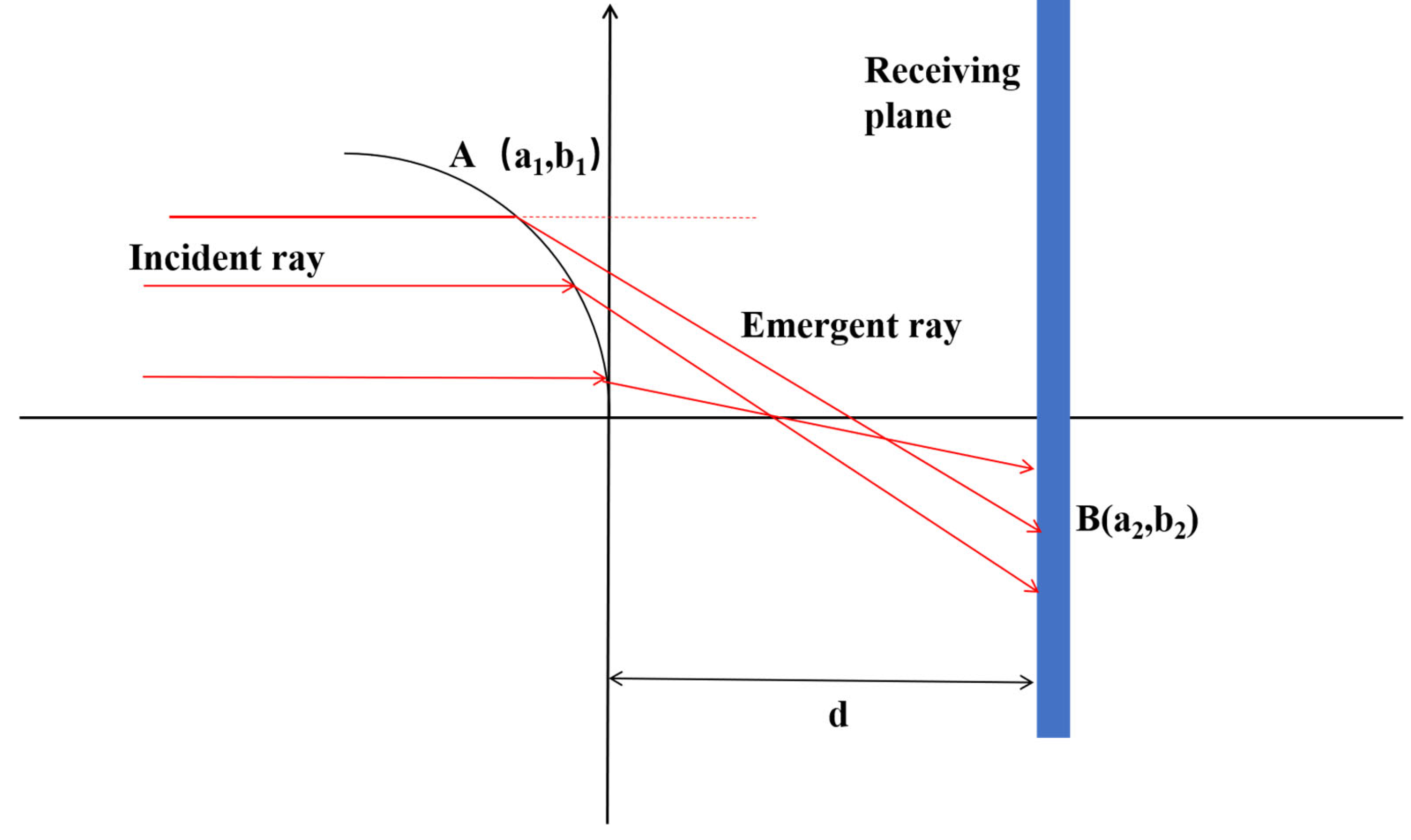
Figure 1 is a schematic diagram of the light propagation of a free-form surface microlens. Based on this set of ideas, we derive the differential equation of the mirror surface. We use parallel light passing through a lens for analysis. The top of the microlens is located at the coordinate origin, and the lenses are symmetrically distributed. Suppose parallel light passes through a lens with a radius of
r1 and then is distributed on a plane with a radius of
r2. The distance between the lens and the plane receiving the light is
d, and the distance between the lens and the light source is
l = 30 mm. The contact point between the incident light and the lens is point a. After refraction by the lens, the emergent light intersects the plane receiving the light at point b, and the angle between the emergent light and the
z-axis is
θ. Suppose the coordinates of point a are (
a1,
b1) and those of point b are (
a2,
b2). From this, we can obtain the incident vector
m = (0,
b1 − a), the emergent vector
n= (
a2 − a1,
d − b1), and
l = (
−db1,
da1), where
b1 and
a1 are the derivatives of the freeform surface components in the directions of b and a, respectively, and
k is the refraction coefficient of the lens.
According to the law of refraction,
and since the relationship between
a1 and
a2 is
then substituting the above several formulas into Formula (7) yields
Finally, it is simplified to obtain
The final result is the differential equation of
a1 and
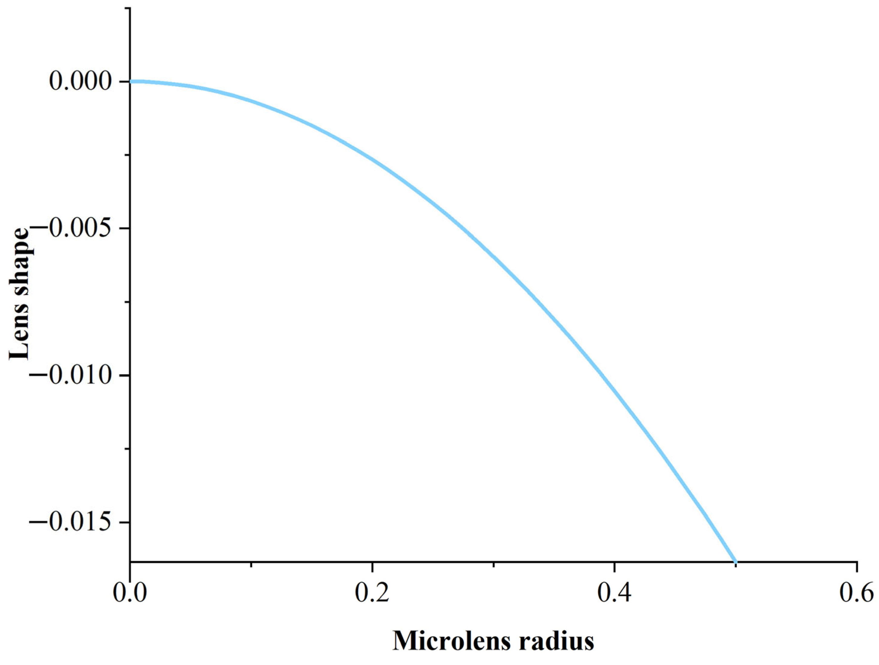
b1. By solving it with the MATLAB software R2022a, the cross-sectional curves can be obtained, as shown in
Figure 2.
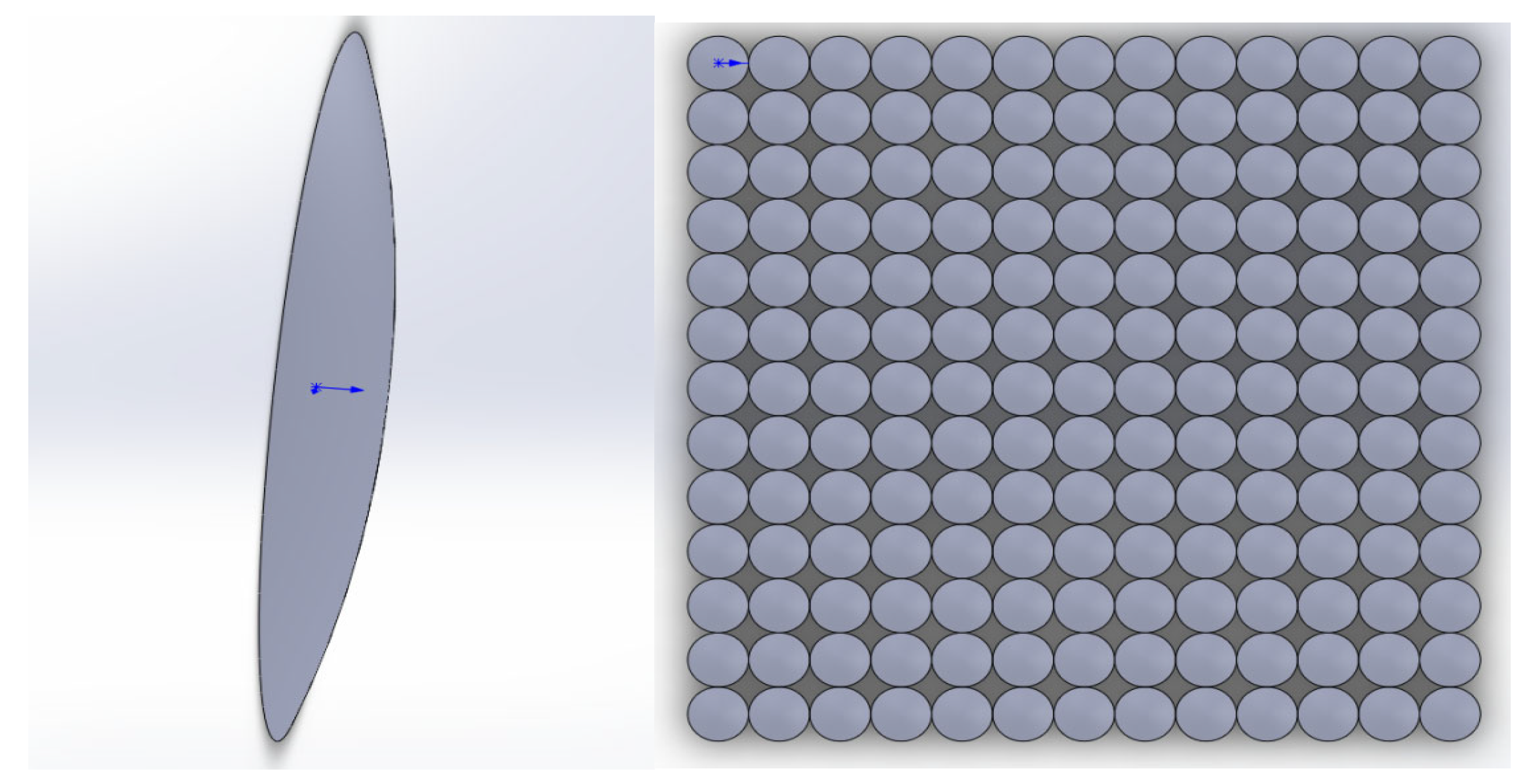
After obtaining the lens curve, the curve equation is imported into Solidworks 2020, and the lens and microlens arrays as shown in
Figure 3 are generated by scanning and using an array. Then import the generated lens array into the Tracepro software 20.0.03 for optical simulation. After designing the material of the lens using Tracepro 20.0.03, the Lamberian light source was adopted for simulation. By adjusting the parameters of the number of lens arrays, the size of
r2, and the distance between the lens and the receiving plane, and comparing them using the Taguchi method, the optimal uniform illumination solution was obtained.
In the use of microlens arrays, it is difficult to layout and utilize these arrays. To facilitate the use of microlens arrays, a mechanical structure platform is built using Solidworks. There is space above the platform, allowing the microlenses to be installed in an array. Install LED light sources at the bottom of the mechanical structure to enable the entire uniform lighting system to be well presented in this mechanical structure.
3. Optical Simulation and Analysis of the Lighting System
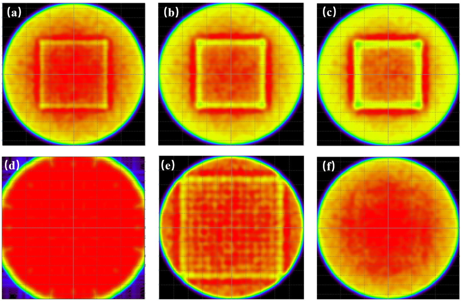
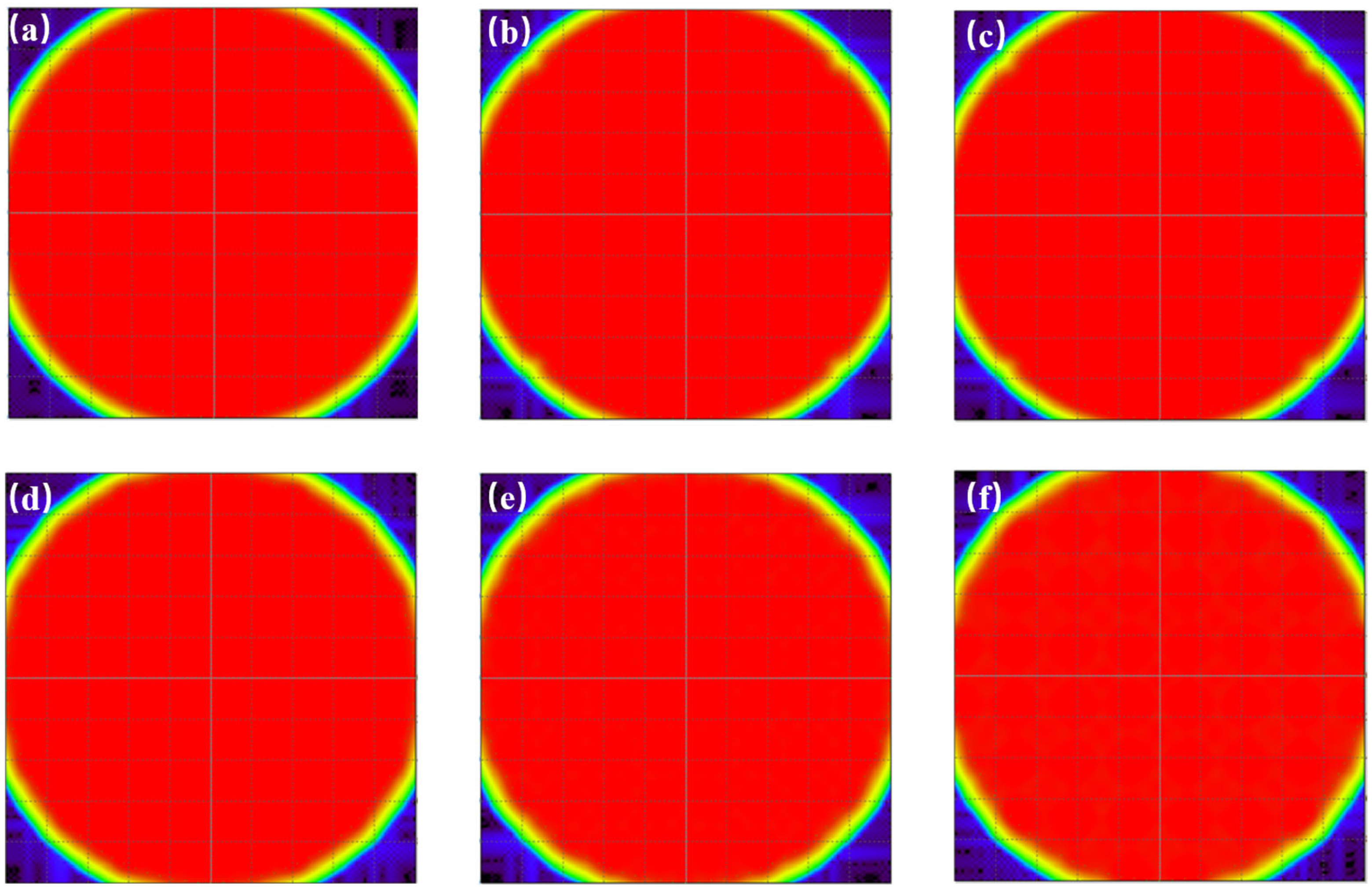
During the Tracepro optical simulation process, the simulation components were built from left to right in sequence: Lambert LED light source–microlens array–receiving light source surface. After the optical component system was built, the receiving plane material was set up to make it a good absorption plane, thereby reducing the reflection of light. During the simulation process, ray tracing can obtain the ray simulation results. It can be seen that the light source generated by the LED light source completely passes through the microlens array and is completely received by the receiving plane. After conducting another simulation, in order to obtain the optimal uniform illumination result, the method of controlling variables was adopted. By controlling the number of microlens arrays, the radius of the lens array, and the distance between the lens array and the receiving plane, the relevant influencing factors were found, as shown in
Figure 4,
Figure 5,
Figure 6 and
Figure 7.
As can be seen from
Figure 4, an LED chip with a size of 1 mm × 0.2 mm × 1 mm is adopted. The luminous power efficiency of the chip is 90 lm/W, the power is 1 W, and the initial number of luminous surfaces is set to 10,000,000. By setting the size of all of the microlens arrays to 13 × 13 and controlling the distance between the microlens arrays and the receiving plane to 300 mm, the simulation experiments were conducted by adjusting the radius sizes of the lenses in the microlens array to 0.5 mm, 1 mm, 1.5 mm, 2 mm, 2.5 mm, and 3 mm, respectively. It can be clearly seen that the change in the radius size of the lenses in the lens array also has a significant impact on the lighting effect.
As can be seen from
Figure 5, the ray tracing simulation is carried out by using the same LED chip and adjusting the same number of rays. By setting the radius of the lens in the microlens array to 2 mm and the distance between the microlens array and the receiving plane to 300 mm, and by setting the number of microlens arrays to 11 × 11, 12 × 12, 13 × 13, 14 × 14, 15 × 15, and 16 × 16, it can be seen from the simulation results obtained in
Figure 5 that different numbers of microlens arrays can achieve different uniform illumination results. When the number of microlens arrays selected is 13 × 13, its uniform illumination effect is better. When the number of arrays is larger or smaller, there is still room for improvement in its uniform illumination effect. Seek the optimal uniform illumination solution among the number of 13 × 13 microlens arrays.
As can be seen from
Figure 6, the number of LED chips and light rays adopted remains unchanged. By setting the radius of the lens in the microlens array to 2 mm and setting the microlens array to 13 × 13, and by changing the distances between the microlens array and the receiving plane to 100 mm, 200 mm, 300 mm, 400 mm, 500 mm, and 600 mm, respectively. It can be seen that the uniform illumination is better when the distance is changed, but there are differences in the illumination efficiency.
It can be seen that different distances between the lens array and the plane receiving the light will correspond to different lighting effects. Therefore, the number of microlens arrays, the size of the lens radius, and the distance between the lens array and the plane receiving the light can be set as different variable factors to seek the optimal lighting result. After obtaining the simulation results, the Taguchi method is adopted to analyze the experimental results using orthogonal arrays. In order to solve the optimization of issues such as quality, cost, and processing with higher performance and a more systematic approach, Taguchi and Konishi proposed the Taguchi comparative trial and error method [
18,
19,
20]. Because the algorithm is highly practical, the processing of the results in this time is also carried out using the Taguchi method. The use of orthogonal arrays can significantly reduce the development time and cost, thereby increasing its competitiveness.
To better observe the relevant conditions of the optimal results, this paper uses the Tracepro software program to conduct multiple simulation modeling analyses. As shown in
Figure 7, it can be clearly observed that the optimal situation is when the microlens array is 13 × 13, the lens radius is 2 mm, and the distance between the lens array and the receiving plane is 300 mm, at which point the illumination uniformity is the best. The optimal uniform lighting result has a uniformity of 98.9% and a lighting efficiency of 93.7%.
