Article

Ultra-Broadband Solar Absorber Design Covering UV to NIR Range Based on Cr–SiO2 Metamaterial Planar Stacked Structures

1
School of Civil Engineering, Jiaying University, Meizhou 514015, China
2
Department of Chemical and Materials Engineering, National University of Kaohsiung, Kaohsiung 811, Taiwan
3
Department of Aeronautical Engineering, Chaoyang University of Technology, Taichung 413, Taiwan
4
Department of Business Administration, Chaoyang University of Technology, Taichung 413, Taiwan
*
Authors to whom correspondence should be addressed.
Photonics 2025, 12(9), 907; https://doi.org/10.3390/photonics12090907
Submission received: 18 June 2025 / Revised: 13 August 2025 / Accepted: 9 September 2025 / Published: 10 September 2025

Abstract

This paper presents the design of an ultrabroadband solar absorber, developed using a metamaterial stack composed of only two materials, consisting of alternating layers of Cr and SiO2. Starting with a Cr layer as the substrate, multiple pairs of Cr and SiO2 were stacked sequentially, where one Cr layer and one SiO2 layer constitute a single pair. To further enhance performance, a cylindrical Cr structure was added to the top. A key innovation of this work lay in its material simplicity and cost efficiency, relying solely on two inexpensive materials, Cr and SiO2. Additionally, the inclusion of the top Cr cylinder was found to significantly enhance absorptivity. Simulations demonstrate that removing this feature led to a noticeable reduction in absorptivity of approximately 10% across the 500–2000 nm wavelength range. Another important finding is the effect of the number of Cr–SiO2 pairs on absorption behavior. When the number of pairs increases from four to five, the average absorptivity decreases slightly, but the absorption bandwidth is notably broadened. Further increasing six pairs resulted in a marginal increase in bandwidth, while maintaining the average absorptivity. Moreover, a low-absorptivity dip at 360 nm was slightly mitigated, rising to approximately 0.900. Based on these insights, a six-pair metamaterial structure was chosen for further optimization. Utilizing COMSOL Multiphysics® simulation software (version 6.0), the absorber was successfully engineered to achieve high performance across an exceptionally broad spectral range, from 200 nm to 2160 nm. Under optimal design parameters, it exhibited an average absorptivity of 0.950, with absorptivity consistently exceeding 0.900 throughout this range. This demonstrates the absorber’s strong potential for efficient solar energy harvesting using a structurally simple and cost-effective design.

1. Introduction

Recent advancements in metamaterial absorbers have evolved along several distinct paths, each tailored to meet specific application demands. These include the design of narrowband absorbers for enhanced sensing precision [1,2], multi-band absorbers capable of achieving perfect absorption at discrete frequencies [3,4,5], and absorbers optimized for high absorptivity within the solar spectrum to improve solar energy harvesting efficiency [6,7]. Among these developments, achieving ultra-wideband (UWB) absorption with near-unity absorptivity remains a critical goal for applications such as stealth technology, thermal imaging, and broadband energy harvesting. To this end, extensive research has been conducted to explore various physical mechanisms and structural strategies that enable UWB absorption. One promising approach involves the use of multilayer planar metamaterials. These structures typically consist of stacked 2D metasurfaces with tailored geometries and material properties, enabling the manipulation of electromagnetic responses across a broad range of frequencies. Planar-type metamaterials offer several advantages, such as ease of fabrication using standard lithography or printing techniques, compatibility with flexible substrates, and the potential for large-area integration. However, they also face inherent limitations, particularly in achieving UWB performance.
Because planar resonant elements often exhibit narrowband behavior due to their strong frequency selectivity, designing a flat structure that supports continuous and efficient absorption over a wide frequency range is particularly challenging. Consequently, realizing UWB absorption in planar configurations often requires sophisticated multi-layer designs, hybrid resonance modes, or the integration of gradient index profiles. A representative example is the work by Cui et al., who demonstrated an infrared absorber based on a sawtooth-patterned anisotropic metamaterial, showcasing the potential of geometry-driven broadband response [8]. However, achieving similar performance using strictly planar and multilayered configurations requires careful optimization of interlayer coupling and impedance matching across the target spectrum [9,10,11,12]. In this work, we explore the design of an ultra-wideband absorber based on multilayer planar metamaterials, aiming to overcome the intrinsic narrowband limitations of planar structures while maintaining the practical benefits of ease of fabrication and integration. This study lies in the development of an ultra-wideband absorber operating in the near-infrared range from 200 nm to 2160 nm, achieved solely through the use of alternating layers of Cr and SiO2. The absorber is based on a multilayer planar metamaterial architecture, designed to overcome the intrinsic narrowband limitations typically associated with planar structures, while preserving the advantages of simple fabrication and compatibility with large-area integration. The primary reason for selecting Cr in this study lies in its high extinction coefficient across the visible to near-infrared spectral range, which enables strong light absorption [13,14].
Its metallic properties also confer excellent electrical conductivity and optical loss characteristics. Cr exhibits a moderate real part of the refractive index (n ≈ 3–4) and a relatively large imaginary part (k ≈ 3–5), which further enhances its absorptive capability—an essential feature for achieving ultrabroadband absorption. Compared to noble metals such as Au and Ag, Cr is significantly more cost-effective and compatible with widely used physical deposition techniques, including evaporation and sputtering. Nearly all optical absorbers—whether based on planar thin films or other specialized structures—are fundamentally nanostructured. The fabrication of such nanoscale structures typically relies on semiconductor processing techniques. Among the major cost factors in semiconductor fabrication are the use of high-vacuum equipment and high-purity materials. One critical aspect often overlooked is the stark cost difference between noble and non-noble metals. For instance, the price of Ag is approximately USD 1.2 million per metric ton, which is more than 100 times that of Cr (USD 12,000 per metric ton), while Au is even more expensive—reaching up to USD 105 million per metric ton, over 9000 times the cost of Cr. While photolithography processes are often assumed to be cost-prohibitive, their actual impact on overall fabrication costs is relatively modest. When used in planar configurations, the addition of photolithography and photoresist steps typically increases costs by less than 10%. The primary expenses still lie in vacuum-based deposition and the fabrication of photomasks—both of which can be reused multiple times. When amortized, the dominant cost driver becomes the material itself, making the choice between noble and non-noble metals a critical consideration for practical applications.
The SiO2 layer serves as an optical path modifier that optimizes light distribution within the absorber, enhancing overall absorption efficiency through strategic alteration of reflection and refraction patterns in multilayer configurations. SiO2 is selected as the complementary material due to its near-perfect transparency across the solar spectrum (k ≈ 0) and low refractive index (n ≈ 1.46), which creates a strong refractive index contrast with Cr. In the multilayered interleaved structure, SiO2 functions as an optical spacer layer that works synergistically with Cr to generate absorption peaks through interference effects, effectively broadening the absorption bandwidth while minimizing reflection losses. This anti-reflection mechanism ensures maximum light transmission into the absorber, significantly enhancing the net solar energy absorptivity. The practical advantages of SiO2 include its ease of processing and cost-effectiveness, making it widely adopted in semiconductor and optical device fabrication [15,16]. The Cr–SiO2 interleaved multilayer stack enables the superposition of multiple interference and absorption resonance modes, resulting in broadband absorption, near-perfect absorptivity, and tunable spectral response through precise control of layer thickness and number. The introduction of surface structures—such as Cr cylindrical nanostructures—further enhances the absorptive performance and tunability of the system.
To further validate the absorber’s performance, additional analyses were conducted, including optical impedance matching and polarization-dependent responses under transverse electric (TE) and transverse magnetic (TM) modes. These results confirm that the absorber facilitates efficient energy coupling into the material with minimal reflection and loss. Electromagnetic field distributions were also analyzed to identify the dominant absorption mechanisms, revealing that both propagating surface plasmon polaritons and localized surface plasmon resonances contribute to the enhanced absorptivity, depending on the operating wavelength. These insights provide a deeper understanding of the physical mechanisms governing light absorption in the proposed metamaterial structure. In this work, although conventional simulation methodologies are employed, the core novelty lies in the structural design and the ability to finely tune geometric and material parameters to achieve an ultra-broadband absorption spectrum. Specifically, the proposed absorber demonstrates high absorptivity (greater than 0.900) over an extended bandwidth that exceeds 200 nm and reaches into the ultraviolet (UV) region. This expanded high-efficiency absorption range not only ensures effective solar energy harvesting but also enables applicability in UV-sensitive domains such as ultraviolet photodetectors and optical sensing devices. Such spectral extension is rarely observed in conventional designs, which typically focus on solar or infrared regions. The unique multilayer configuration and the engineered interplay between materials and nanostructure geometry contribute to strong resonance effects and enhanced field confinement across a broader spectrum. This tunable and multifunctional design thus provides a significant advancement beyond existing absorber structures.

2. Structure of the Investigated Ultrabroadband Solar Absorber with Cr–SiO2 Metamaterial Stacked Structures

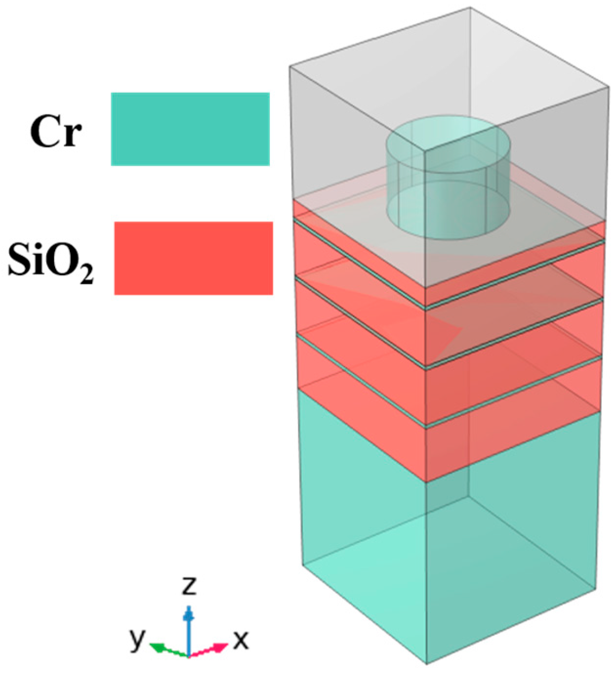
In this study, an ultrabroadband solar absorber was successfully designed using a metamaterial stack composed of two inexpensive materials, Cr and SiO2. The intricate geometric architecture of the unit cell (with p = 300 nm) of the investigated multi-layered metamaterial absorber is meticulously detailed in Figure 1, revealing a sophisticated eleven-layer configuration designed for optimal electromagnetic wave absorption. For our optical absorber design, we utilized the material properties of Cr and SiO2 directly from COMSOL’s (version 6.0) built-in material database, including their complex refractive indices, absorption coefficients, wavelength-dependent optical dispersion curves n(λ) and k(λ), and dielectric constants. The structure exhibits precisely engineered layer thicknesses: a foundational Cr layer of 300 nm (h1) as the substrate, followed by alternating layers of SiO2 and Cr. The four SiO2 layers (h2, h4, h6, and h8) were each set at 85 nm, and the thickness of the topmost SiO2 layer h10 was reduced to 28 nm, while the four Cr layers (h3, h5, h7, and h9) each measured 6 nm. For the five-pair structure, the h8 and h9 layers were omitted, while for the four-pair structure, the h6, h7, h8, and h9 layers were excluded, as illustrated in Figure 2. The investigated absorbers without the topmost Cr cylinder are shown in Figure 2a and those with the topmost Cr cylinder are shown in Figure 2b. All three structural configurations were topped with a cylindrical Cr structure with a thickness h11 of 100 nm and a diameter d of 165 nm. h1 to h10 all belonged to a continuous planar structure, and the period P was set to 300 nm as the basic unit for analysis.
The polarization direction of the incident light used to identify the optimal geometric configuration of the designed optical absorber was set normal to the top-layer material, oriented along the negative z-axis. This simple yet effective design was modeled and optimized through comprehensive numerical simulations using COMSOL Multiphysics® (version 6.0), commercial finite element analysis software. Simulation results reveal that removing the topmost Cr cylinder results in an approximately 10% drop in absorptivity across the 500–2000 nm wavelength range, underscoring its critical role in absorption enhancement. To further optimize the absorber’s performance, systematic parametric sweep analyses were conducted to explore the effects of geometric variations on absorption efficiency and electromagnetic response. Each structural parameter was varied individually while keeping others constant to determine the optimal configuration.
Additionally, the number of Cr–SiO2 pairs was investigated. Increasing the number of pairs from four to five slightly reduced average absorptivity but significantly broadened the absorption bandwidth. Further increasing the number from five to six yielded modest additional bandwidth enhancement while maintaining nearly constant average absorptivity. This work highlights not only the material and structural simplicity of the proposed absorber but also its effectiveness in achieving high optical performance across an ultrabroadband and spectrum. The Cr–SiO2 metamaterial under investigation, composed of six stacked Cr–SiO2 pairs, was modeled using a mesh structure with the following specifications: comprising 26,388 grid nodes with grid lengths varying from 0.80 nm (minimum) to 1.60 nm (maximum). This mesh included 147,710 tetrahedral elements, 24,648 triangular elements, 56 endpoint elements, and 1264 edge finite elements. The overall mesh quality was reflected in an average element quality of 0.6292 and a minimum quality of 0.1873. With an element volume ratio of 1.593 × 10⁻⁴ and a total grid volume of 7.965 × 10⁷ nm3, the mesh configuration provided a robust foundation for achieving reliable and accurate simulation results.
The absorption and impedance values presented in this study were obtained through numerical simulations using COMSOL Multiphysics® software (version 6.0). Specifically, the electromagnetic wave frequency domain interface was employed to solve Maxwell’s equations and model the interaction of incident light with the designed metamaterial absorber structure. Absorptivity was calculated based on the following relation:
A(λ) = 1 − R(λ) − T(λ)
where R(λ) and T(λ) represent the reflectance and transmittance at a given wavelength, respectively. Since the bottom Cr layer is optically thick, the transmittance T(λ) was negligible, allowing absorptivity to be approximated as A(λ) ≈ 1 − R(λ). Impedance values were extracted from the complex reflection coefficient obtained via the simulation results. The normalized impedance (Z) was calculated using the following relation:
Z(λ) = [(1 + r(λ)]/[1 − r(λ)]
where r(λ) is the complex reflection coefficient at each wavelength. The closer the real part of Z is to 1 and the imaginary part to 0, the better the impedance matching with free space, which enhances absorptivity.
It is important to emphasize that the proposed broadband solar absorber is specifically designed for low- to moderate-temperature solar energy applications, with an intended operating range below 300 °C and an absorption spectrum covering 200–2160 nm. This spectral range encompasses the majority of solar irradiance under AM1.5 conditions and is highly relevant to practical applications such as solar steam generation, photothermal conversion at sub-300 °C temperatures, and photovoltaic-integrated thermal systems. Within this temperature range and for non-concentrated solar input, radiative losses in the mid- to far-infrared region (λ > 2.5 µm) are inherently minimal due to the negligible absorption beyond the cut-off wavelength, making further optimization of spectral selectivity and long-wavelength emissivity unnecessary for achieving high energy efficiency. Given this clearly defined application scope, our study prioritizes optimizing solar absorptivity in the UV-NIR regime, where performance gains directly impact the target use cases. While the mid-IR emissivity spectrum could in principle be estimated from reflectance data via Kirchhoff’s law, these data were not included because emissivity beyond 2.5 µm has a negligible influence under our operational conditions. For high-temperature or high-concentration applications such as concentrated solar power (CSP), where temperatures frequently exceed 500 °C and radiative losses scale strongly with T4, additional engineering measures, such as introducing specialized spectral-selective coatings or modified multilayer configurations, would be necessary to suppress long-wavelength emissivity [17,18,19].
These adaptations lie outside the present scope but are identified as potential future directions. Furthermore, although the absorber incorporates Cr and SiO2—materials with differing thermal expansion coefficients—the sub-300 °C operating limit ensures that thermo-mechanical stresses remain well within acceptable bounds, preserving structural integrity throughout its service life in the intended low- to moderate-temperature scenarios. In our previous work, we successfully fabricated absorbers using physical vapor deposition techniques, achieving nanometer-scale precision. The fabricated absorber achieved average absorptivity of 0.956 and 0.962 in the 280–4000 nm range across two measurements, with deviations of only 1.23% and 0.62%, respectively, from the simulated value of 0.968 [20]. Although some variations in layer thickness inevitably occur during fabrication, the resulting deviations are within an acceptable range when compared to simulation results [21]. Both simulation and experimental results demonstrated consistently high absorptivity (>90%) over broad spectral ranges, specifically from 346 to 1971 nm and 315 to 1914 nm, respectively. These results indicate that the simulated and fabricated absorbers achieved bandwidths of 1625 nm and 1599 nm within the high-absorptivity regime. The peak absorptivity values reached 0.996 at 384 nm for the simulation and 0.995 at 546 nm for the experimental measurement.

3. Investigations of the Optimal Parameters for Each Layer of the Investigated Ultrabroadband Solar Absorber

3.1. Effect of Varying Cr–SiO2 Pairs on Absorption Characteristics and Optical Impedance

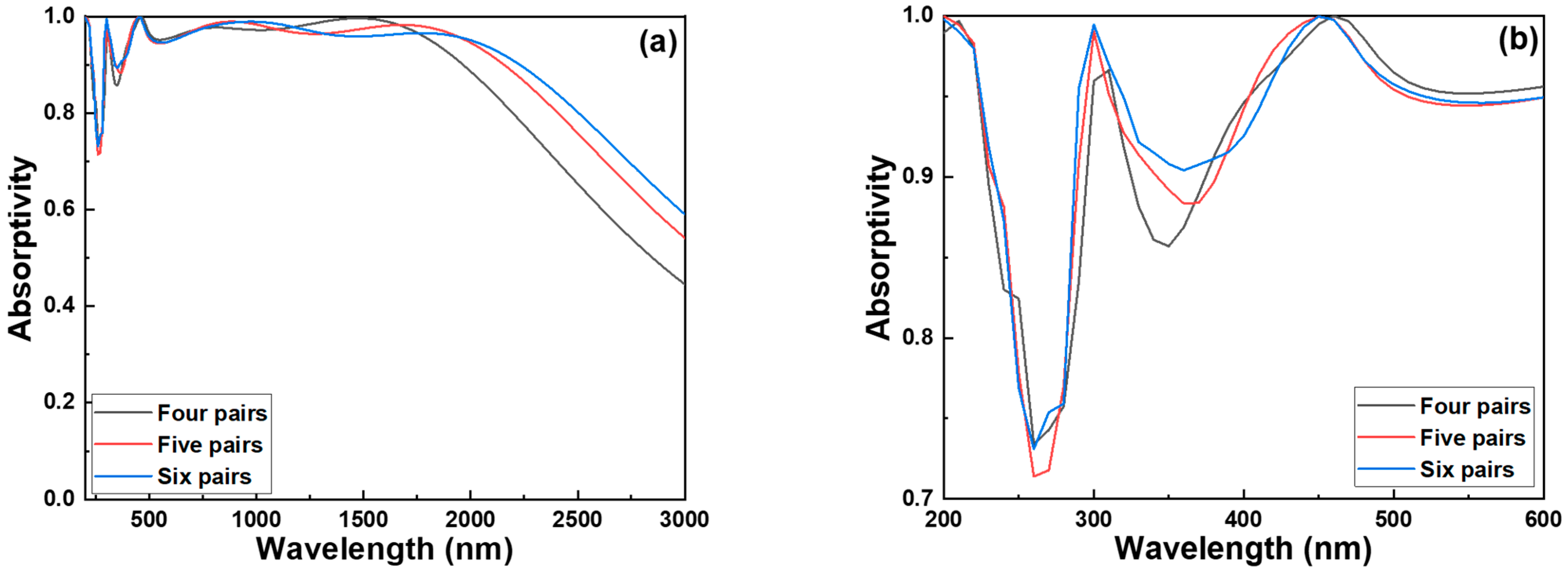
To evaluate the influence of layer configuration on absorption performance, we first compared the spectral characteristics of three absorber structures composed of different numbers of Cr–SiO2 pairs. As the number of Cr–SiO2 pairs increased from four to five, a trade-off phenomenon was observed: the average absorptivity experienced a slight decline; however, this was effectively offset by a substantial enhancement in operational bandwidth, as Figure 3a shows. This behavior can be attributed to the increased optical path length and interference effects introduced by the additional layers, which enhance the constructive interference over a broader wavelength range while slightly affecting peak absorption. Further increasing the number of Cr–SiO2 pairs from five to six yielded even more promising results. The average absorptivity remained nearly constant, while the absorption bandwidth continued to improve. This improvement is primarily due to the multilayer interference and impedance matching effects, which facilitate better suppression of reflection across a wider spectral range. At a wavelength of approximately 465 nm, these absorbers exhibit the characteristics of a perfect absorber (absorptivity~1), as shown in Figure 3b. In the structure with four Cr–SiO2 pairs, absorptivity began to drop at approximately 1900 nm, limiting the effective absorption range.
However, when the number of pairs increased to six, the high-absorptivity region (absorptivity > 0.900) extended from 1900 nm to around 2200 nm, indicating a redshift of the absorption band. This redshift can be explained by the increased effective optical thickness, which shifts the resonance conditions toward longer wavelengths. In addition to the improvements in the near-infrared region, increasing the number of Cr–SiO2 pairs also resulted in a noticeable enhancement in the ultraviolet to visible range (200–500 nm). Notably, the absorption dip at 360 nm—originally below the 0.900 threshold—was mitigated, with the absorptivity slightly exceeding 0.900. This indicates that the multilayer structure helps flatten the absorption spectrum and reduce spectral valleys through enhanced field confinement and multilayer interference. Based on these optimization studies, the six-pair Cr–SiO2 metamaterial absorber emerges as the most favorable configuration for achieving broadband absorption performance. Under carefully optimized parametric conditions, the absorber maintains high absorptivity (>0.900) across a wide wavelength range from 500 nm to 2160 nm, demonstrating excellent spectral coverage. Nevertheless, the current six-pair design has not yet achieved optimal performance in the sub-500 nm region. Further structural optimization—such as fine-tuning layer thicknesses or introducing additional nanoresonant features—will be necessary for enhancing absorptivity beyond 0.900 in this short-wavelength range, ensuring truly uniform ultra-broadband absorption.
In the field of optical absorber research and applications, an absorptivity threshold greater than 0.900 is commonly adopted as the standard criterion for defining the effective absorption bandwidth. This definition arises primarily from the high-performance requirements in practical applications such as infrared stealth, solar thermal conversion, and photodetection. In these scenarios, achieving high absorptivity (A > 0.900) ensures that the majority of the incident electromagnetic energy is effectively absorbed, minimizing reflection, transmission, and signal loss. Such a level of performance typically corresponds to the behavior of a near-perfect absorber, which serves as a benchmark in both experimental and simulation-based designs. Moreover, using 0.900 as a unified threshold facilitates consistent comparisons across different studies and absorber designs, enabling a standardized basis for evaluating performance. If the absorptivity falls below 0.900—such as 0.800—the absorber’s effectiveness is significantly compromised. At absorptivity = 0.800, up to 20% of the incident energy is not absorbed, leading to notable energy loss. This can negatively affect various applications: in solar thermal devices, it results in reduced heat conversion efficiency; in stealth technologies, the remaining reflected or transmitted signals may still be detectable by radar or infrared sensors; and in photovoltaic systems, it reduces light utilization and limits power conversion efficiency. Additionally, absorbers with lower absorptivity may fail to provide sufficient energy concentration or field enhancement in applications requiring strong resonance or thermal localization, such as sensors or thermal emitters. The optical selectivity is also weakened, as the absorber may no longer exhibit high absorption in the target band while maintaining low reflectance elsewhere, thereby diminishing its utility in filtering and stealth-related applications.
Achieving an ultra-broadband absorption range spanning from 200 to 2160 nm using a simple bilayer structure is extremely rare and scarcely reported in the current literature. In this work, we demonstrate that by utilizing straightforward material combinations such as Cr–SiO2, it is possible to realize such an exceptionally wide absorption bandwidth without the need for complex structural designs. While several previous studies have attempted to enhance the absorption bandwidth using Cr–SiO2 [22,23] or W–SiO2 [24,25] systems, either alone or in combination with other materials, these configurations generally fall short of extending absorption into the deep-ultraviolet region. To achieve broader coverage, especially in the short-wavelength infrared or deep-ultraviolet ranges, these approaches often rely on additional layers or nanostructured geometries, which significantly complicate fabrication. Although various sophisticated designs have been proposed to push absorption boundaries further, extending the spectral response down to 200 nm typically requires intricate multi-layered or resonant architectures. In contrast, our ability to attain this broadband performance through a relatively simple and fabrication-friendly design highlights both the novelty and the practical potential of our approach. To demonstrate the critical role of the top Cr metal cylinder in our absorber design, we modified the original structure shown in Figure 1 by removing this top component, resulting in a new configuration illustrated in Figure 2a.
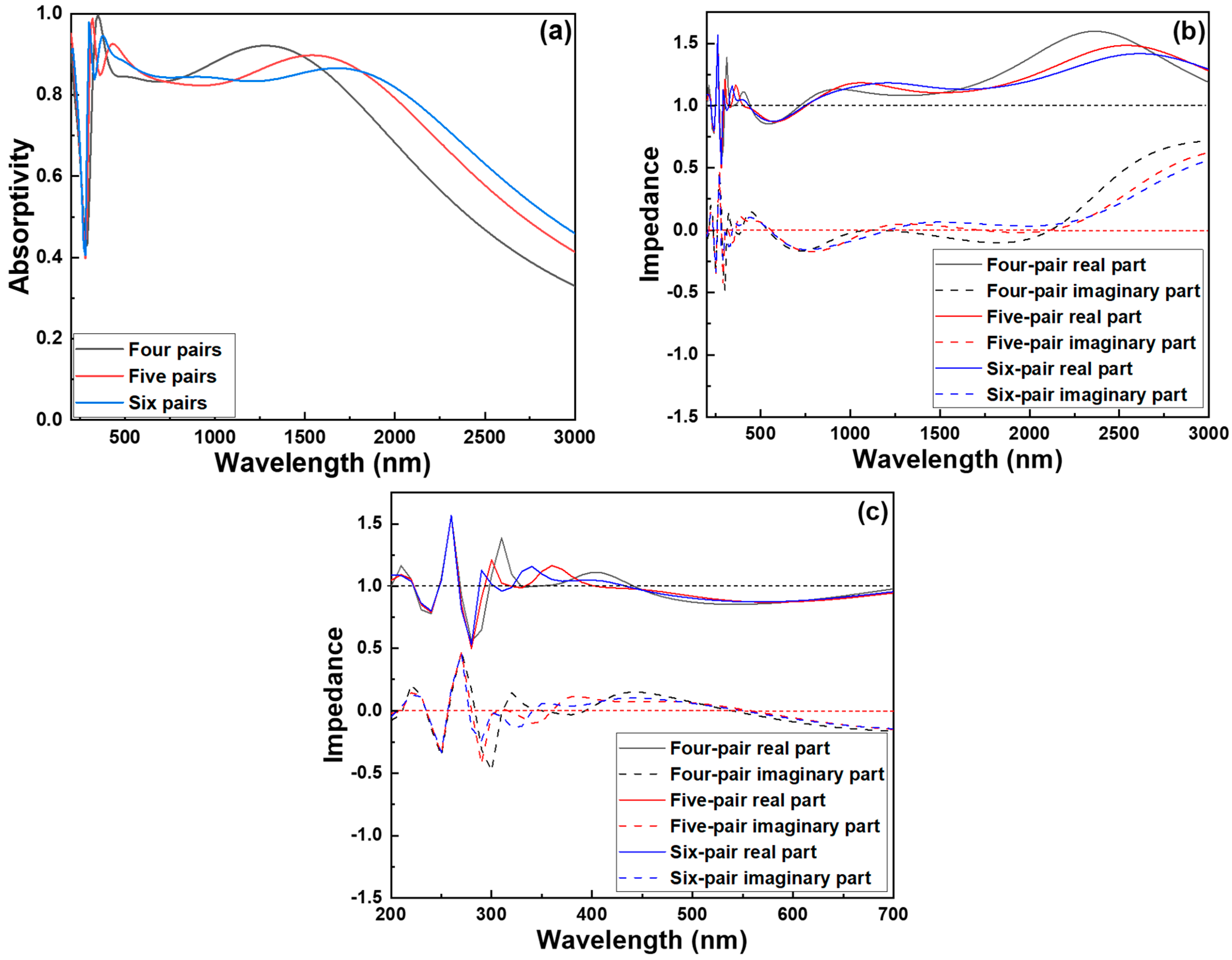
We then evaluated and compared the absorptivity of three different absorber types without the top Cr cylinder to the original structures that retained it. As shown in the simulation results in Figure 4a, the removal of the top Cr cylinder causes a substantial drop in absorptivity across all three structures. Notably, in the ultraviolet wavelength range of 200–300 nm, the absorptivity sharply declines to around 0.4, indicating that the top Cr metal cylinder plays a pivotal role in enhancing the absorption characteristics of the system, especially in the UV region. This significant reduction in absorptivity can be attributed to the disruption of optical and electromagnetic interactions within the structure. The top Cr metal cylinder likely supports plasmonic resonance and facilitates impedance matching with free space, both of which are essential for efficient light trapping and energy dissipation. Its removal eliminates these beneficial effects, leading to increased reflection and reduced energy coupling into the absorber. To investigate the underlying physical mechanism responsible for this performance degradation, we conducted an optical impedance analysis of the structure depicted in Figure 4a. The results, shown in Figure 4b, reveal that the real part of the optical impedance deviates substantially from 1, while the imaginary part diverges significantly from 0 after the top Cr cylinder is removed. The real part of the impedance characterizes the degree of impedance matching with free space. When this value strays far from unity, it indicates a strong mismatch, causing considerable reflection of incident light at the interface and reducing the amount of energy that penetrates the absorber.
This mismatch disrupts the critical coupling condition necessary for optimal energy absorption. The imaginary part of the impedance represents the phase relationship between the electric and magnetic fields within the material and is closely associated with intrinsic loss or reactive energy storage. A large deviation from zero in the imaginary component suggests the presence of strong capacitive or inductive behavior, leading to excess energy being stored rather than dissipated as heat. Such behavior not only prevents efficient energy conversion but also contributes to further internal reflections, exacerbating the overall loss. Taken together, these results confirm that the absence of the top Cr metal cylinder undermines the absorber’s ability to effectively capture and dissipate incident electromagnetic energy. The Cr cylinder contributes not only to enhancing absorption through localized field enhancement and resonance effects but also to maintaining favorable impedance conditions. Its removal severely impairs the optical properties of the absorber, underscoring its indispensable role in achieving high-performance absorption, particularly in the ultraviolet regime. Nevertheless, even with the inclusion of the top Cr metal cylinder and six pairs of Cr–SiO2 layers, the absorber still fails to achieve high absorptivity in the ultraviolet range (200–400 nm) under the current parameter settings.
Figure 4c shows an expanded view of the impedance spectra of the investigated absorbers in the 200–700 nm wavelength range. As illustrated, in the region below 280 nm, the impedance values for all three structures remain nearly constant, indicating minimal spectral variation in that range. However, once the wavelength exceeds 280 nm, the six-pair structure designed in this study exhibits a real part of impedance that is closer to 1 and an imaginary part closer to 0 compared to the other two configurations. This behavior suggests that the six-pair structure achieves more effective impedance matching with free space across a wider portion of the spectrum, starting from relatively short wavelengths. Such improved matching is critical for enhancing absorption efficiency, particularly in the deep ultraviolet to visible regions, and demonstrates the advantage of the six-pair design in achieving ultra-broadband absorption. Therefore, we aim to perform parameter optimization on the six-pair Cr–SiO2 structure to enhance its absorption performance, with the goal of achieving high absorptivity within the UV spectrum.

3.2. Analysis of the Optimal Structural Parameters for Each Layer of Cr–SiO2 Pairs and the Top Cr Cylinders

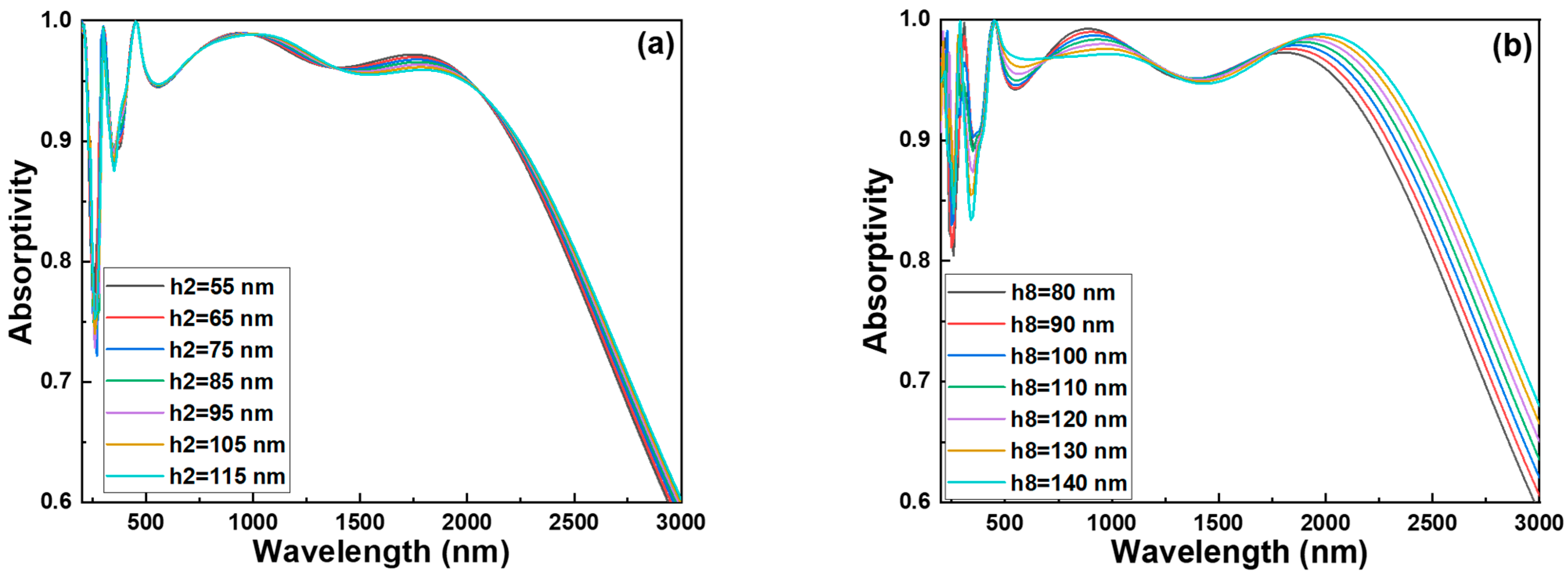
To determine the optimal thickness for each individual layer in the multilayer structure, we conducted a step-by-step simulation process. In this procedure, we varied the thickness of one specific layer at a time while keeping the thicknesses of all other layers fixed. This approach allowed us to isolate and examine the influence of each layer on the overall optical absorptivity. We began by analyzing the bottommost layer, designated as the h2 SiO2 layer. Figure 5a displays the absorption spectra as a function of layer thickness (y-axis) and wavelength (x-axis). The color scale indicating the absorptivity is typically shown on the right side of each figure. For example, in Figure 5a, the right-side color bar shows that dark red represents an absorptivity of 1.000, while the color gradually transitions to blue, indicating an absorptivity of 0.500. All subsequent similar figures follow the same convention. As shown in Figure 5a, changes in the thickness of this layer had only a minor impact on the overall absorptivity. A slight variation was observed near a wavelength of approximately 250 nm. When the thickness was adjusted to 55 nm, the 2D absorptivity map indicated a clear reduction in the yellow region near 250 nm, which corresponds to higher absorption. Therefore, we selected 55 nm as the optimal thickness for the h2 SiO2 layer to enhance absorption performance at this specific wavelength. With the h2 SiO2 layer fixed at 55 nm, we proceeded to examine the effect of the h4 SiO2 layer, positioned higher in the structure. Similar to h2, the h4 SiO2 layer had a relatively subtle influence on the total absorptivity, while the detailed data are not presented in this section. However, a closer look revealed that a thickness of 70 nm resulted in a noticeable improvement in absorption near 270 nm, making 70 nm the most suitable thickness for the h4 SiO2 layer.
Next, we analyzed the h6 SiO2 layer, which is even closer to the air interface and to the direction of incident light. Although we do not present the detailed results here, the trends observed were generally consistent with those of the h2 and h4 layers—mainly affecting localized absorption but having a limited impact on the overall profile. Interestingly, the behavior of the h6 layer resembled that of the h8 SiO2 layer, whose performance is illustrated in Figure 5b. In the case of h8, which lies just beneath the outermost SiO2 layer, the influence on absorptivity was far more pronounced, especially in both the short and long wavelength regimes. Specifically, for wavelengths below 500 nm, two distinct absorption valleys were observed. Around 380 nm, the absorptivity exceeded 0.9 when the thickness of the h8 SiO2 layer reached or surpassed 110 nm. In the long-wavelength range—particularly beyond 2000 nm—absorptivity increased progressively with the thickness of the h8 SiO2 layer. However, this trend was not consistent across all spectral regions. For instance, an absorption peak near 880 nm exhibited a decrease in absorptivity as the thickness increased. Based on this analysis, we selected 110 nm as the optimal thickness for both the h6 and h8 SiO2 layers.
The more significant influence of upper layers such as h6 and h8, particularly in the short and long wavelength regions, can be attributed to their physical proximity to the incident light source and the air interface. At shorter wavelengths, the optical penetration depth of incident light is relatively shallow, meaning that the interaction between the light and the topmost layers is stronger. Any change in thickness in these layers can significantly alter the conditions for interference and reflection, affecting how efficiently light is absorbed or reflected. In the long-wavelength regime, while light penetrates deeper into the structure, the top layers still play a critical role due to the phase accumulation over the optical path. Constructive and destructive interference effects become more pronounced as the optical path length increases with wavelength. Therefore, even subtle variations in the thickness of the upper layers can shift the phase conditions for these longer wavelengths, enhancing or suppressing absorption depending on the specific structural configuration. Moreover, the fact that the upper SiO2 layers lie beneath one more SiO2 layer (i.e., they are not the very topmost layer but still near the top) means that their optical effect is influenced by multi-layer interference within a semi-transparent stack. This layered interference can enhance the field localization at certain resonant wavelengths, thereby increasing the optical energy density and leading to enhanced absorption either in underlying lossy layers or at specific resonant points. These complex interactions explain why the h6 and h8 layers exhibit greater influence across both spectral extremes, and why their optimization is crucial for achieving high-performance broadband absorptivity.
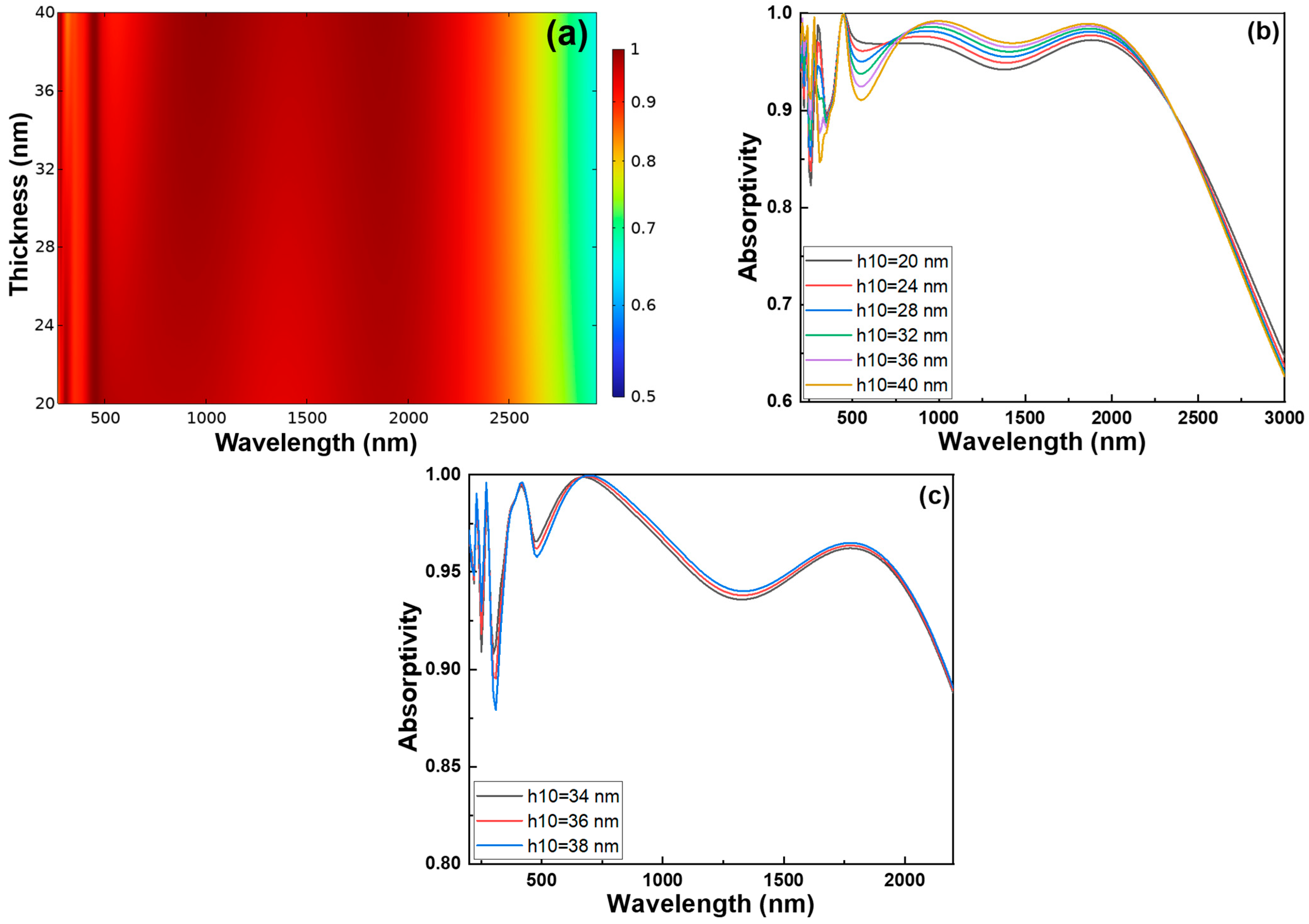
Finally, we performed a thickness sweep of the h10 SiO2 layer, which is located beneath the Cr matrix-arranged cylindrical structures. We conducted a detailed thickness sweep of the h10 SiO2 layer, which lies beneath the Cr cylindrical matrix structure, and observed distinct variations in absorptivity across different wavelength regions. As shown in Figure 6a, when the thickness of the h10 SiO2 layer increases, absorptivity decreases in the 300–370 nm and 500–850 nm ranges, but increases within the 200–290 nm ultraviolet region. This contrasting behavior is primarily attributed to the interference effects and the optical path length within the multilayer structure. At shorter wavelengths (200–290 nm), light penetration depth is shallow, and the increasing thickness of the SiO2 layer enhances the near-field coupling between the Cr nanocylinders and the underlying layers, as well as constructive interference, thereby improving absorption. In contrast, at longer wavelengths (300–370 nm and 500–850 nm), destructive interference becomes more dominant with increasing SiO2 thickness, resulting in reduced absorptivity due to phase mismatches and weakened field confinement at the absorber-active interfaces. The goal of adjusting the h10 SiO2 thickness was to maximize absorption in the deep UV range while minimizing the loss of absorption in the visible range, as shown in Figure 6b. However, Figure 6b also reveals that in some cases, even with thickness optimization, the absorptivity fails to exceed 0.9, which is the target threshold for high-efficiency absorbers in the UV region. To finetune the optimal thickness, we performed a refined sweep in the 34–38 nm range, incrementing by 2 nm. As shown in Figure 6c, within this range, increasing thickness still leads to improved absorption in the 200–290 nm UV region, due to enhanced field localization and better resonance conditions, but simultaneously causes a drop in visible light absorption, likely due to increased reflection and destructive interference. Considering the trade-off between enhancing UV absorptivity and maintaining acceptable performance in the visible range, a final thickness of 34 nm was selected as the optimal configuration, achieving better balance across the spectrum.
Next, we analyzed the influence of different Cr metal layers on the absorption properties of our designed absorbers. We began by investigating the effect of varying the thickness of the h3 Cr layer. As shown in Figure 7a, increasing the thickness of the h3 Cr layer has a relatively minor impact on the overall absorptivity. However, as the metal thickness increases, a gradual decrease in absorptivity is observed around the wavelengths of 250 nm and 360 nm. Based on this trend, a thickness of 6 nm was determined to be the optimal parameter for the h3 Cr layer. We then examined the effect of varying the h5 Cr layer thickness on absorption. According to Figure 7b, increasing the h5 Cr thickness results in a noticeable decrease in absorptivity beyond 2000 nm, indicating a blue shift in the spectral region where absorptivity remains above 0.9. Additionally, absorptivity near 270 nm and 360 nm also gradually decreases with increasing thickness. Therefore, 6 nm was again selected as the optimal thickness for the h5 Cr layer. Although we do not present the detailed results here, the analysis of the h7 Cr layer also reveals that increasing the Cr thickness leads to a broader region of low absorptivity at longer wavelengths, represented by expanded blue and yellow areas in the absorption maps—further evidence of a pronounced blue shift. Around 250 nm, absorptivity also decreases progressively, with the yellow (low absorptivity) regions becoming more prominent. Among the data, the 6 nm thickness clearly provides the best absorptivity performance, making it the most suitable choice for the h7 Cr layer as well.
Finally, Figure 7c,d present the absorptivity distribution map and absorption spectra for different h9 Cr layer thicknesses. These figures clearly demonstrate that the thickness of the h9 Cr layer significantly influences the absorption behavior. As the Cr layer becomes thicker, regions of low absorptivity at longer wavelengths expand, again showing a marked blue shift. Based on the results in both figures, the h9 Cr layer also achieves optimal absorption performance at a 6 nm thickness. The observed variations in absorptivity with respect to different Cr layer thicknesses can be directly attributed to the optical characteristics of the multilayer structure, which consists of alternating SiO2 and Cr layers on a 300 nm Cr substrate (h1). In this configuration, the optimal thicknesses of four SiO2 layers of h2, h4, h6, and h8 are found to be 55, 70, 110, and 110 nm, while the corresponding Cr layers (h3, h5, h7, and h9) are set to the same thicknesses of 6 nm, and the topmost SiO2 layer (h10) is thinner at 34 nm. Additionally, Cr nanocylinders are patterned on the top surface. This layered design creates multiple interference interfaces and plasmonic interactions that govern the absorption characteristics. As Cr is a lossy metal, its thickness plays a crucial role in modulating both reflection and absorption across different wavelengths.
When the Cr layers (h3, h5, h7, and h9) are thin (around 6 nm), they contribute to constructive interference and enhanced field confinement, leading to high absorption across a broad spectral range. However, increasing their thickness reduces the transmission of incident light into deeper layers and leads to stronger reflection or damping, particularly at specific wavelengths. For instance, the decreasing absorptivity near 250 nm and 360 nm, observed with increasing Cr thickness in h2 and h4 regions, is due to the enhanced reflectivity and phase mismatches introduced by thicker metallic layers. The blue shift in high absorptivity regions (noted beyond 2000 nm) occurs because increased metal thickness alters the effective optical path and shifts the resonance conditions, especially in the h4, h6, and h8 Cr layers. This effect is amplified in upper layers closer to the incident light, as they more directly modulate the interaction of light with the structure. Thus, maintaining the Cr layer thickness at 6 nm ensures an optimal balance between sufficient absorption and minimal reflection or damping losses, enabling strong absorptivity over both short and long wavelength ranges.
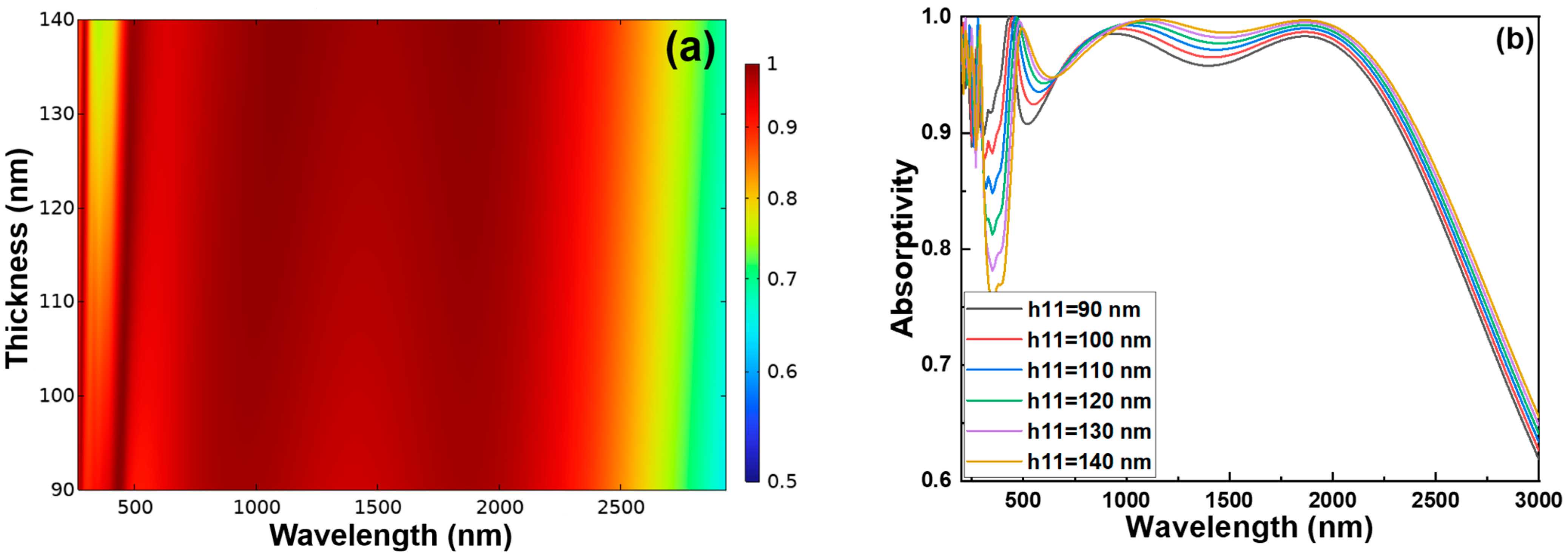
An optimization analysis was conducted on the cylinder height of the H11 Cr layer. As the height of the cylindrical structure increases, notable changes in optical absorption characteristics are observed. According to the 2D color map shown in Figure 8a, an increase in cylinder height leads to a decrease in absorptivity within the wavelength range of 300–500 nm. This is visually represented by the expansion of the yellow low absorptivity region on the map. Furthermore, the absorption spectra in Figure 8b confirm this trend: as the cylinder height increases, the overall absorption significantly decreases, particularly in the targeted wavelength range. Based on these observations, a cylinder height of 90 nm is determined to be the optimal value, balancing structural design with efficient optical performance.
Finally, we conducted an optimal width analysis for the cylindrical diameter d of the h11 Cr layer. As the cylinder diameter increases from 90 nm to 170 nm, it is evident that absorptivity improves significantly in the wavelength ranges of approximately 200–320 nm and 600–1350 nm. However, when the diameter exceeds 120 nm, a decreasing trend in absorptivity is observed in the 430–700 nm range. This trend is also visually apparent in the 2D color map, where the red regions become lighter, as shown in Figure 9a,b, further illustrating the variation in the absorption spectra for diameters ranging from 110 nm to 150 nm. It is clear that as the diameter increases, the absorption in the longer wavelength region—where absorptivity exceeds 0.9—expands. However, this improvement comes with a trade-off: a noticeable drop in absorptivity around the 500 nm valley. For diameters of 110 nm and 120 nm, absorptivity at the 310 nm absorption dip remains below 0.9. In contrast, when the diameter increases to between 130 nm and 150 nm, absorptivity in the ultraviolet region surpasses 0.9 across the entire UV range. According to Figure 9b, the configuration with a diameter of 130 nm demonstrates the most balanced and highest average absorptivity across the broad wavelength range of 200–2160 nm, indicating the most efficient overall absorption performance. Therefore, a cylinder diameter of 130 nm is identified as the optimal design parameter for the H11 Cr layer.
In this study, the topmost array of Cr cylinders plays a crucial role in enhancing absorption within the 200–350 nm wavelength range. By tuning the height and diameter of these cylinders, the structure can achieve an effective optical impedance with a real part close to 1 and an imaginary part near 0. This improvement in absorption arises from several key mechanisms. First, the Cr cylinder array behaves as an effective medium layer; by adjusting the diameter and spacing of the cylinders, the effective refractive index of the layer can be finely controlled, enabling a gradual impedance transition from air (n = 1) to the underlying layers. Second, the Cr cylinders support localized surface plasmon resonances within the ultraviolet range. When the cylinder dimensions resonate with the target wavelengths, strong electromagnetic field localization occurs, intensifying the light–matter interaction. Third, the periodic cylinder array induces strong scattering, which increases the optical path length within the structure. The scattered light undergoes multiple reflections within the multilayer architecture, creating a light-trapping effect that prolongs the interaction time between light and the absorbing materials. Fourth, the alternating SiO2 and Cr layers themselves form an interference cavity, enhancing absorption at specific wavelengths through constructive interference. The metallic Cr cylinders on top further couple with this interference field, boosting local field intensity and absorption. Lastly, the lower SiO2/Cr multilayer acts as a Fabry–Perot cavity, where the thicknesses of the SiO2 layers are precisely designed to match the target wavelengths.

3.3. Comparison of Absorption Spectra Before and After Structural Modification and the Principle of Optical Impedance

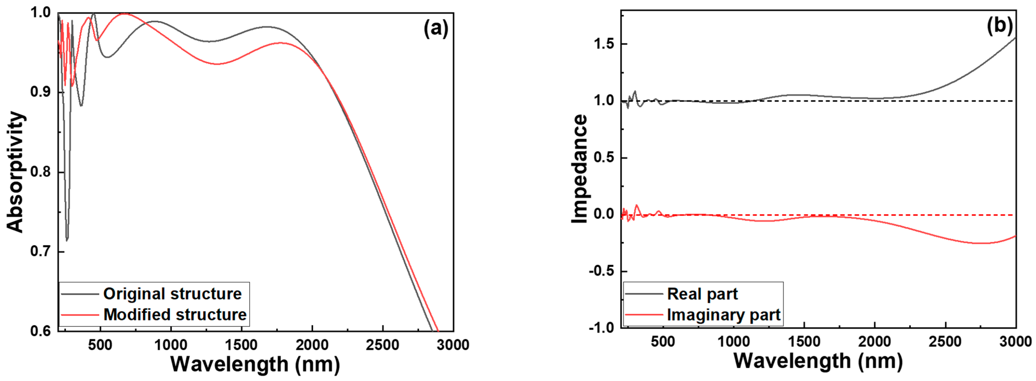
Based on the preceding series of analyses, the optimal thicknesses for the SiO2 layers—h2, h4, h6, h8, and h10—were determined to be 55 nm, 70 nm, 110 nm, 110 nm, and 34 nm, respectively. The corresponding Cr layers—h3, h5, h7, and h9—were each optimized to a uniform thickness of 6 nm. Additionally, the cylindrical Cr nanostructures positioned on the topmost h11 Cr layer exhibited a height of 90 nm and a diameter d of 130 nm. Figure 10a compares the absorption spectra of the original structure with that of the fully optimized absorber. Although the optimized absorber exhibits slightly reduced absorption in the longer wavelength range of 1000–2000 nm, it shows significant enhancement in absorptivity for wavelengths below 900 nm. This improvement is particularly prominent in the ultraviolet region, where the enhanced multilayer configuration—especially the addition of precisely tuned metal–dielectric pairs and the Cr cylindrical nanostructures—promotes stronger light confinement, increased resonance effects, and more efficient energy dissipation. These optimizations collectively contribute to superior performance in the UV and visible spectra, which are critical for applications such as photodetectors and solar absorbers. Figure 10b presents the optical impedance analysis of the absorber with the optimized structural parameters. Compared with the impedance profile shown in Figure 4b, it is evident that the imaginary part of the impedance in the optimized absorber remains close to zero until approximately 2050 nm, after which it begins to shift noticeably toward negative values.
Similarly, the real part of the impedance remains close to 1 until around 2300 nm, beyond which it starts to deviate significantly and bends toward higher values. This behavior indicates that the optimized absorber maintains well-matched impedance with free space (Z0 ≈ 1) across a broader spectral range, thereby minimizing reflection and maximizing absorption in the UV to near-infrared regions. The delayed deviation of the imaginary part toward negative values suggests that the structure effectively suppresses reactive (non-dissipative) components of the impedance over a wide wavelength range, reducing phase mismatch and enhancing light coupling. Meanwhile, the shift in the real part toward higher values at longer wavelengths reflects increased resistive losses and impedance mismatching, which reduce absorption efficiency in the far-infrared range. These changes are primarily caused by the cumulative effects of material dispersion, interference within the multilayer stack, and the frequency-dependent effective permittivity and permeability of the engineered nanostructure. To elucidate the perfect absorption mechanism of the proposed ultra-broadband solar absorber based on Cr–SiO2 metamaterial planar stacked structures, impedance matching theory is employed. The effective impedance Z is calculated using the following expression, where S11 and S21 represent the reflection and transmission coefficients, respectively [26,27]:
z = ( 1 +   S 11 ) 2   S 21 2 ( 1 +   S 11 ) 2 +   S 21 2
The absorptivity (A) can be expressed as follows:
A = 1 S 11 2   S 21 2
When the structure is designed such that Re(Z) ≈ 1 and Im(Z) ≈ 0, the effective impedance of the absorber matches that of free space. This eliminates impedance mismatch, minimizing reflection and enabling near-perfect absorption of the incident electromagnetic waves. Figure 10b shows that the designed absorber exhibits characteristics of Re(Z) ≈ 1 and Im(Z) ≈ 0 in the 200–2160 nm range. As a result, the absorber achieves an absorptivity greater than 0.900 within this wavelength range.

3.4. Simulated Spatial Distributions of Electric and Magnetic Field Intensities

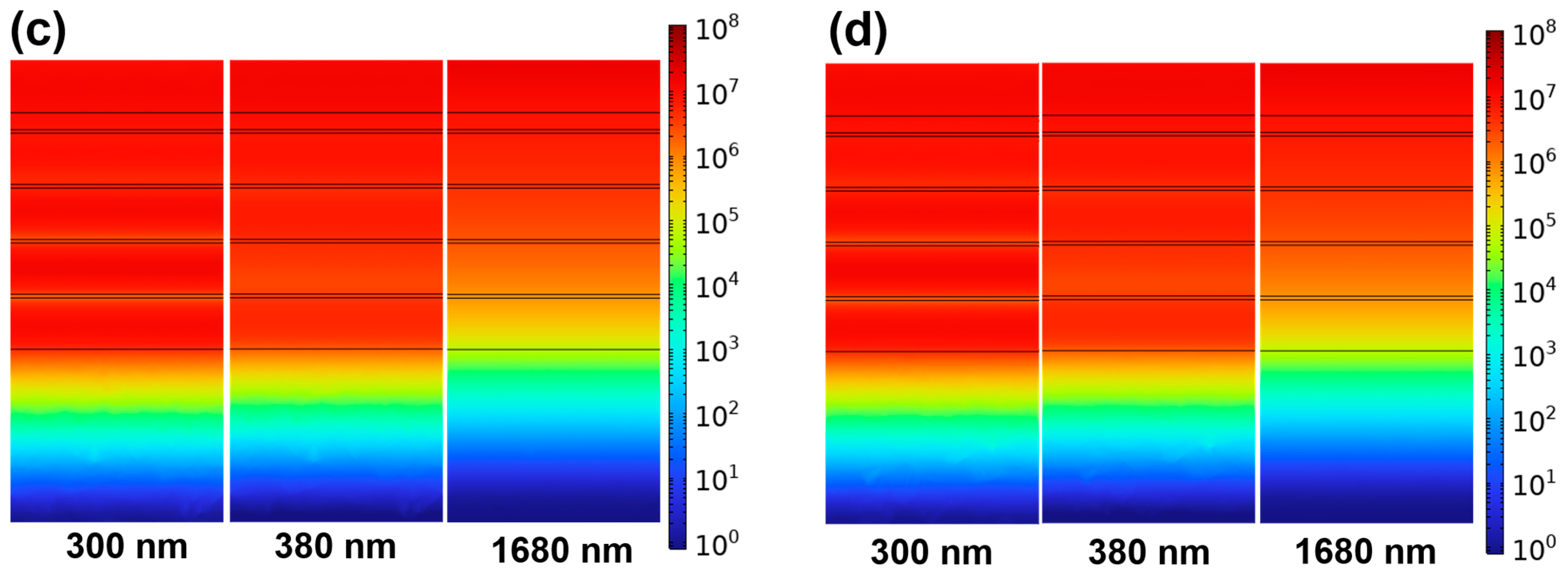
In this study, the ultra-wideband optical absorber under investigation is specifically engineered to achieve high light absorption across an extensive spectral range, from 200 nm in the ultraviolet-C region to 2160 nm in the near-infrared region. Figure 11 presents the simulated electric and magnetic field distributions at selected wavelengths of 420, 670, and 1780 nm, as shown in Figure 11a and Figure 11b, respectively. First, Figure 11a,b clearly demonstrate the high absorptivity characteristics of the top Cr cylinder layer at wavelengths of 420 nm and 670 nm, and the low absorption characteristic at a wavelength of 1780 nm. This observation supports our earlier assertion that the top Cr cylindrical structure plays a crucial role in enhancing the absorption performance of the entire design, particularly in the shorter wavelength range. The electric field intensity distribution in Figure 11a indicates strong field localization, correlating with high absorption at shorter wavelengths. Furthermore, as the wavelength increases, the regions of peak electric field intensity—and thus strong absorption—tend to shift toward the upper layers of the structure. This spatial shift is consistent with the wavelength-dependent nature of surface plasmon resonances (SPRs), which are more tightly confined at shorter wavelengths and more delocalized at longer wavelengths. Moreover, although the electric field intensity—and by extension, the absorptivity—slightly decreases as the wavelength increases from 420 to 1780 nm, the drop is not drastic.
Notably, at a wavelength of 1780 nm, the electric field intensity within the Cr cylinder becomes weaker than that in the surrounding dielectric regions. This phenomenon can be attributed to the wavelength-dependent behavior of SPRs. At longer wavelengths, such as 1780 nm, the excitation of localized surface plasmons is less efficient, resulting in reduced confinement of the electromagnetic field within the metallic nanostructure. Additionally, the increased skin depth at longer wavelengths allows the incident electromagnetic wave to penetrate deeper into the structure, causing the field to spread more broadly into the surrounding layers rather than being concentrated within the Cr cylinder itself. Despite the weaker field localization at this wavelength, the absorber still maintains considerable absorptivity, as energy dissipation continues to occur in the dielectric–metal interfaces and other lossy components of the multilayer structure. However, the magnetic field analysis in Figure 11b reveals a more noticeable trend: as the wavelength increases, the overall region within the structure exhibiting high absorption becomes narrower and more superficial. In particular, between 670 and 1780 nm, the high-absorptivity zones not only become shallower but also decrease in spatial extent, as evidenced by the expansion of regions with lower field intensity (i.e., “origin regions”). These findings indicate a gradual reduction in the absorber’s efficiency at longer wavelengths.
Nevertheless, the results confirm that the dominant mechanism enabling broadband absorption across the full 200–2160 nm range is SPR. SPR arises from the collective oscillation of free electrons at the interface between the metal (Cr) and dielectric materials, which strongly enhances local electromagnetic fields and, consequently, absorption. The observed decline in absorptivity at longer wavelengths can be attributed to the shift in resonance conditions; specifically, as the incident wavelength approaches the mid-infrared region, the efficiency of SPR diminishes due to the lower confinement of plasmonic modes and reduced coupling strength. To address the possibility of non-negligible transmission due to the relatively thin multilayer structure and Cr substrate, we provide additional clarification based on the field absorption distribution results shown in Figure 11a,b. It can be clearly observed that the bottom h1 Fe layer exhibits consistently low absorptivity across all wavelengths, as indicated by the prominent blue regions. This suggests that the incident electromagnetic waves are effectively absorbed by the upper layers before reaching the bottom layer, and that almost no significant energy penetrates through the entire structure. Therefore, the transmission through the absorber can be considered negligible. These results validate that the high absorptivity is primarily attributed to the efficient absorption and resonance effects within the multilayer system, rather than any transmitted component. The electric and magnetic field intensities for the six-pair structure without the topmost Cr cylinder (as shown in Figure 2a) are presented in Figure 11c,d. Notably, these intensities are significantly weaker compared to those observed in the six-pair structure with the topmost Cr cylinder.
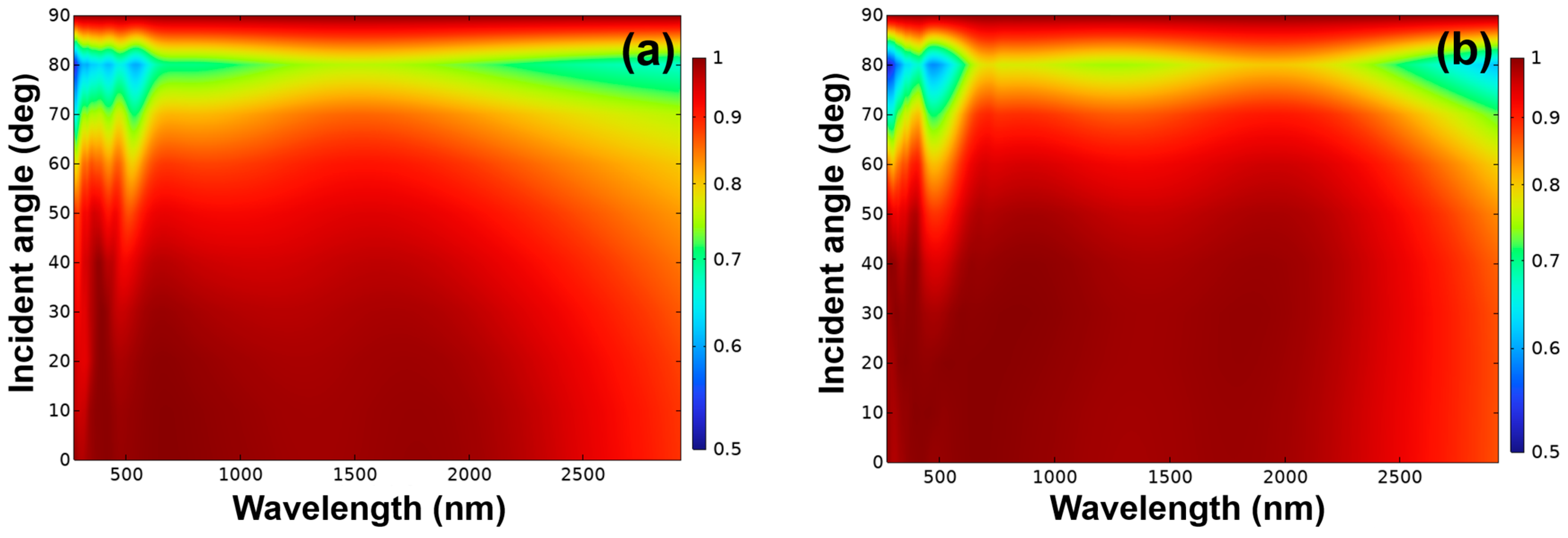
We conducted a comprehensive evaluation of the absorption performance of the proposed metamaterial absorber across the full electromagnetic spectrum, spanning from the ultraviolet-C band at 200 nm to the near-infrared region up to 2160 nm. The assessment considered incident angles ranging from 0° to 90°, and included both transverse electric (TE) polarization, as shown in Figure 12a, and transverse magnetic (TM) polarization, as shown in Figure 12b. As illustrated in Figure 12, there is no significant difference in absorptivity between TE and TM polarizations, indicating polarization-insensitive behavior. The simulation results further reveal the variation in absorptivity as a function of both incident angle and wavelength. The absorber structure is composed of 11 alternating layers. The bottom layer (h1) is a continuous planar Cr film, where layers h3, h5, h7, and h9 consist of continuous planar Cr structures, while h2, h4, h6, and h8 are continuous s SiO2 dielectric layers. The topmost layer features an array of discontinuous cylindrical Cr nanostructures. Absorptivity is angle-dependent and varies as the incident light angle changes from 0° to 90°. For both TE and TM polarizations, a lower absorptivity is observed across most angles in the broadband wavelength range of 200–2500 nm. However, a high absorptivity is consistently observed within the wavelength range of 200 nm to approximately 2300 nm, particularly for incident angles between 0° and 45°. These results demonstrate that the proposed ultra-broadband solar absorber, based on Cr–SiO2 metamaterial planar stacked structures, exhibits excellent angular insensitivity. This makes it a promising candidate for practical solar energy harvesting applications where variable light incidence is a key consideration.
3.5. Comparison with Other Research Results and Potential Applications

The Cr cylinders, functioning as metallic nanostructures, play a crucial role in enhancing the optical performance of the absorber. They excite localized surface plasmon resonances (LSPRs) at specific wavelengths, amplifying the local electromagnetic field and improving light-matter coupling efficiency. In addition, they form a resonant cavity with the underlying multilayer structure, inducing interference-based resonance through multiple reflections of incident light. These combined mechanisms significantly enhance absorption, particularly at targeted spectral bands. Simulation results show that removing the topmost Cr cylinder leads to an approximate 10% drop in absorptivity across the 500–2000 nm range and reduces a local absorptivity peak near 360 nm from approximately 0.900, confirming its critical role in light trapping. Based on these findings, a six-pair Cr–SiO2 configuration was selected for further optimization. Under optimal design parameters, the proposed absorber achieves absorptivity exceeding 0.900 across the entire 200–2160 nm spectrum, with an impressive average absorptivity of 0.950 and a peak absorptivity of 0.999 at 670 nm. To highlight the advantages of this design, Table 1 compares its performance with several recently reported ultra-wideband absorbers. Unlike conventional planar optical absorbers, which often struggle to sustain high absorption in the deep ultraviolet (200–300 nm) region, and unlike other designs that require complex geometries or expensive noble metals like Au, our absorber employs only Cr and SiO2—both low-cost and compatible with standard semiconductor fabrication processes. This structurally simple yet highly efficient absorber demonstrates exceptional broadband absorption using scalable and practical materials, making it a promising candidate for solar energy harvesting applications.
To clarify the operational mechanism and practical value of the proposed absorber, we highlight several potential application scenarios. Owing to its broadband absorptivity extending from the ultraviolet to the near-infrared, including strong absorption in the 200–300 nm range, the structure is particularly suited for ultraviolet photodetectors, sterilization systems, and accelerated material aging studies, where efficient UV absorption is critical. Although solar irradiance below 300 nm accounts for less than 1.0% of the AM1.5 spectrum and thus contributes negligibly to conventional photovoltaic efficiency, this spectral feature is an inherent result of the multilayer configuration and tailored nanostructure, which enable resonant coupling and localized field enhancement at high photon energies. In addition, the broadband absorption characteristics also make the absorber a strong candidate for solar energy harvesting systems, where maximizing energy conversion across a wide spectral range is essential. These combined attributes demonstrate the design’s versatility and practical relevance across different spectral domains, extending its applicability well beyond traditional photovoltaic scenarios.

4. Conclusions

For the ultrabroadband solar absorber based on Cr–SiO2 metamaterial planar stacked structures, the optimal thicknesses of the SiO2 layers—h2, h4, h6, h8, and h10—were determined to be 55, 70, 110, 110, and 34 nm, respectively. The corresponding Cr layers—h3, h5, h7, and h9—were each optimized to a uniform thickness of 6 nm. Additionally, the cylindrical Cr nanostructures placed atop the uppermost h11 Cr layer had a height of 90 nm and a diameter d of 130 nm. The simulation results clearly demonstrate that the top Cr cylindrical nanostructures exhibit pronounced absorption peaks at wavelengths of 420 nm and 670 nm, and a distinct absorption dip at 1780 nm. These findings reinforce our previous assertion that the top Cr cylindrical layer plays a pivotal role in enhancing the overall absorption performance of the proposed structure, particularly within the short-wavelength region of the spectrum. The designed absorber exhibits distinct absorption peaks at 420 nm, 670 nm, and 1780 nm, along with an ultra-broadband absorption bandwidth ranging from 200 to 2160 nm. It achieves an average absorptivity of 0.950 and a maximum of 0.999 at 670 nm, indicating near-perfect absorption performance. Moreover, consistently high absorptivity is maintained across the 200–2300 nm range, particularly for incident angles between 0° and 45°. These results confirm that the proposed ultra-broadband solar absorber, based on a Cr–SiO2 metamaterial planar stacked structure, demonstrates excellent angular insensitivity.

Author Contributions

Conceptualization, W.-L.H., X.-Y.L., C.-F.Y. and K.-K.L.; methodology, W.-L.H., X.-Y.L., C.-M.H., C.-F.Y. and K.-K.L.; validation, W.-L.H., X.-Y.L., C.-M.H., C.-F.Y. and K.-K.L.; formal analysis, W.-L.H., X.-Y.L., C.-M.H., C.-F.Y. and K.-K.L.; investigation, W.-L.H., C.-F.Y. and K.-K.L.; data curation, W.-L.H., X.-Y.L., C.-M.H., C.-F.Y. and K.-K.L.; writing—original draft preparation, W.-L.H., C.-F.Y. and K.-K.L.; writing—review and editing, W.-L.H., C.-F.Y. and K.-K.L.; visualization, W.-L.H., X.-Y.L., C.-F.Y. and K.-K.L. All authors have read and agreed to the published version of the manuscript.

Funding

The works are supported by Summit-Tech Resource Corp., and by projects under Nos. NSTC 113-2221-E-390-011 and NSTC 114-2622-E-390-001.

Data Availability Statement

The original contributions presented in this study are included in the article. Further inquiries can be directed to the corresponding author.

Acknowledgments

We would like to thank Pitotech Co., Ltd. for their help in teaching the use of COMSOL Multiphysics® software (version 6.0).

Conflicts of Interest

The authors declare no conflicts of interest.

References

  1. Farooq, S.; Rativa, D.; Said, Z.; Araujo, R.E. Ultra-sensitive narrow-band plasmonic perfect absorber for sensing applications. Photonics Nanostruct. Fundam. Appl. 2022, 50, 101018. [Google Scholar] [CrossRef]
  2. Lateef, O.S.; Al Badri, M.; Al-badri, K.S.L.; Mohammed, S.A. Polarization insensitive Archimedes’ spiral shaped ultrathin metamaterial absorbers for microwave sensing application. Sci. Rep. 2023, 13, 19445. [Google Scholar] [CrossRef] [PubMed]
  3. Dayal, G.; Anantha Ramakrishna, S. Flexible metamaterial absorbers with multi-band infrared response. J. Phys. D Appl. Phys. 2015, 48, 035105. [Google Scholar] [CrossRef]
  4. Anwar, S.; Khan, Q.; Ali, G.; Khan, M.; Maqbool, M. Triple-band terahertz metamaterial absorber with enhanced sensing capabilities. Eur. Phys. J. D 2023, 77, 69. [Google Scholar] [CrossRef]
  5. Errajraji, K.; Jebbor, N.; Das, S.; Islam, T.; Phani Madhav, B.T.; El-Arrouch, T. Design and analysis of a multi-band miniaturized metamaterial absorber for wireless communication applications. Opt. Quantum Electron. 2024, 56, 232. [Google Scholar] [CrossRef]
  6. Devinder, S.; Vishwakarma, M.K.; Joseph, S.; Pandey, S.; Joseph, J. UV-LIG-Based Perfect Broadband Absorber for Solar Thermoelectric Generation. CS Appl. Energy Mater. 2023, 6, 5616–5627. [Google Scholar] [CrossRef]
  7. Peng, G.; Li, W.Z.; Tseng, L.C.; Yang, C.F. Investigation of a Multi-Layer Absorber Exhibiting the Broadband and High Absorptivity in Red Light and Near-Infrared Region. Nanomaterials 2023, 766, 2241003. [Google Scholar] [CrossRef]
  8. Cui, Y.; Fung, K.H.; Xu, J.; Ma, H.; Jin, Y.; He, S.; Fang, N.X. Ultrabroadband Light Absorption by a Sawtooth Anisotropic Metamaterial Slab. Nano Lett. 2012, 12, 1443–1447. [Google Scholar] [CrossRef]
  9. Dinh, M.Q.; Le, M.T.; Ngo, S.T.; Tung, N.T. Unifying approach to multilayer metamaterials absorber for bandwidth enhancement. Opt. Commun. 2021, 485, 126725. [Google Scholar] [CrossRef]
  10. Assal, A.E.; Breiss, H.; Benzerga, R.; Sharaiha, A. Design and optimization of ultra-wideband planar multilayer absorber based on long-carbon fiber-loaded composites. J. Mater. Sci. 2021, 56, 19484–19500. [Google Scholar] [CrossRef]
  11. Peng, G.; Ke, P.X.; Tseng, L.C.; Yang, C.F.; Chen, H.C. The Design of a Multilayer and Planar Metamaterial with the Multi-Functions of a High-Absorptivity and Ultra-Broadband Absorber and a Narrowband Sensor. Photonics 2023, 10, 804. [Google Scholar] [CrossRef]
  12. Rego, D.F.; Silva, F.G.S.; Gusmao, R.C.; Rodriguez-Esquerre, V.F. Design of Planar Multilayer Devices for Optical Filtering Using Surrogate Model Based on Artificial Neural Network. Optics 2024, 5, 121–132. [Google Scholar] [CrossRef]
  13. Kim, I.; So, S.; Rana, A.S.; Mehmood, M.Q.; Rho, J. Thermally robust ring-shaped chromium perfect absorber of visible light. Nanophotonics 2018, 7, 1827–1833. [Google Scholar] [CrossRef]
  14. Iqbal, M.A.; Bakhsh, S.; Maidin, S.S.; Morsy, K.; Choi, J.R.; Alguno, A.C. Investigating structural and optoelectronic properties of Cr-substituted ZnSe semiconductors. Sci. Rep. 2024, 14, 15510. [Google Scholar] [CrossRef] [PubMed]
  15. Lundgaard, S.; Ng, S.H.; Nishijima, Y.; Mazilu, M.; Juodkazis, S. Black Metals: Optical Absorbers. Micromachines 2020, 11, 256. [Google Scholar] [CrossRef]
  16. Khichar, V.; Hozhabri, N.; Koymen, N.A. Solar energy harvesting using new broadband metamaterial solar absorbers for generation of heat. APL Energy 2024, 2, 016105. [Google Scholar] [CrossRef]
  17. Khelifa, A.B.; Khamlich, S.; Nuru, Z.Y.; Kotsedi, L.; Mebrahtu, A.; Balgouthi, M.; Guizani, A.A.; Dimassi, W.; Maaza, M. Growth and Characterization of Spectrally Selective Cr2O3/Cr/Cr2O3 Multilayered Solar Absorber by E-Beam Evaporation. J. Alloys Compd. 2018, 734, 204–209. [Google Scholar] [CrossRef]
  18. De Maio, D.; D’Alessandro, C.; Caldarelli, A.; Musto, M.; Russo, R. Solar selective coatings for evacuated flat plate collectors: Optimisation and efficiency robustness analysis. Sol. Energy Mater. Sol. Cells 2022, 242, 111749. [Google Scholar] [CrossRef]
  19. Farchado, M.; San Vicente, G.; Barandica, N.; Sanchez-Senoran, D.; Morales, A. High performance selective solar absorber stable in air for high temperature applications. Sol. Energy Mater. Sol. Cells 2024, 271, 112849. [Google Scholar] [CrossRef]
  20. Yang, C.F.; Wang, C.H.; Ke, P.X.; Meen, T.H.; Lai, K.K. Design and manufacture of a multi-layer planar solar light absorber with high absorptivity and ultra-wideband from visible light to infrared. Nanomaterials 2024, 14, 930. [Google Scholar] [CrossRef]
  21. Liu, Y.; Ma, W.Z.; You, E.M.; Cai, H.Y.; Zhuang, P.P.; Chen, Y.S.; Liu, J. Optimization configuration of lithograph-free solar energy absorber based on anti-reflection. Sol. Energy 2024, 270, 112417. [Google Scholar] [CrossRef]
  22. Kim, J.H.; Lee, S.G.; Kim, T.T.; Ha, T.; Lee, S.H.; Kim, J.H.; Lee, Y.H. High-temperature differences in plasmonic broadband absorber on PET and Si substrates. Sci. Rep. 2020, 10, 13279. [Google Scholar] [CrossRef] [PubMed]
  23. Lai, F.D.; Lai, Y.T.; Chen, C.-S. Big Data Analysis, Design, Effect Fabrication, and Properties Analysis of SiO2/Cr/SiO2 Colored Solar Selective Absorbers with High PTCE and Chromaticity for Building Applications. Materials 2024, 17, 5810. [Google Scholar] [PubMed]
  24. Zou, Y.; Zhang, C.; Yang, B.; Yi, Z.; Zhang, B.; Wu, X. Lithography-Free Solar Absorber Made of Multilayer W/SiO2 for Efficient Photothermal Conversion. Plasmonics 2023, 18, 1865–1871. [Google Scholar] [CrossRef]
  25. Wang, Y.; Zhang, Y.; Fan, M.; Zhang, J.; Zhou, C. Efficient solar absorber based on VO2–W–SiO2 hybrid metamaterials. Phys. Scr. 2023, 98, 065516. [Google Scholar] [CrossRef]
  26. Zhang, Y.; Hou, B.; Yang, Y.; Song, Q.; Yi, Z.; Zhou, Z. An Active Controllable Wide-Angle and Ultrawideband Terahertz Absorber/Reflector Based on VO2 Metamaterial. Phys. Chem. Chem. Phys. 2024, 26, 6091–6098. [Google Scholar] [CrossRef]
  27. Zhang, Y.; Hou, B.; Song, Q.; Yi, Z.; Zeng, Q. A THz Smart Switch Based on a VO2 Metamaterial That Switches Between Wide-Angle Ultra-Wideband Absorption and Transmission. Dalton Trans. 2024, 53, 19264–19271. [Google Scholar] [CrossRef]
  28. Liu, J.; Ma, W.Z.; Chen, W.; Yu, G.X.; Chen, Y.S.; Deng, X.C.; Yang, C.F. Numerical analysis of an ultra-wideband metamaterial absorber with high absorptivity from visible light to near-infrared. Opt. Express 2020, 28, 23748–23760. [Google Scholar] [CrossRef]
  29. Li, F.; Issah, I.; Baah, M.; Amedalor, R.; Quarshie, M.; Bawuah, P.; Asamoah, B.O. Polarization-dependent wideband met-amaterial absorber for ultraviolet to near-infrared spectral range applications. Opt. Express 2022, 30, 25974. [Google Scholar] [CrossRef]
  30. Rezaei, M.H.; Vatandoust, Y.; Afshari-Bavil, M.; Liu, D. Ultra-broadband, polarization-independent, and wide-angle met-amaterial absorber based on fabrication-friendly Ti and TiO2 resonators. Opt. Quantum Electron. 2024, 56, 400. [Google Scholar]
  31. Li, H.; Qiu, X.; Lu, J.; Tian, X.; Long, H. UV-NIR polarization sensitive metamaterial absorber based on two-dimensional titanium grating. Optik Inter. J. Light Electron Opt. 2024, 311, 171916. [Google Scholar] [CrossRef]
  32. Wang, Y.; Liu, F.; Ni, B.; Chen, L.; Ji, K. Design of an ultra-wideband solar absorber based on tungsten. AIP Adv. 2023, 13, 095024. [Google Scholar] [CrossRef]
  33. Tharwat, M.M.; Alsulami, A.R.; Mahros, A.M. Exploring the Absorption Spectra of an Ultra-Wideband Metamaterial Absorber in the Visible and Near-Infrared Regions. Materials 2022, 15, 7160. [Google Scholar] [CrossRef]
Figure 1. Side view of the three-dimensional and two-dimensional unit cell of the investigated Cr–SiO2 metamaterial stacked structures.
Photonics 12 00907 g001
Figure 2. Side view of the two-dimensional unit cell of the investigated three Cr–SiO2 metamaterial stacked structures, (a) without and (b) with the topmost Cr cylinder.
Photonics 12 00907 g002
Figure 3. Effects of the number of Cr–SiO2 pairs on the absorption spectra, with the topmost Cr cylinder spanning from (a) 200 to 3000 nm and (b) 200 to 600 nm.
Photonics 12 00907 g003
Figure 4. Effects of the number of Cr–SiO2 pairs, without the topmost Cr cylinder, on the (a) absorption spectra, (b) the impedance spectra of the investigated absorbers, and (c) the expanded view of the impedance spectra of the investigated absorbers in the 200–700 nm wavelength range.
Photonics 12 00907 g004
Figure 5. Effects of variations in the thickness of different SiO2 layers on the absorption properties of the designed absorber; (a) thickness of the h2 layer on the absorptivity and (b) thickness of the h4 layer on the absorptivity.
Photonics 12 00907 g005
Figure 6. Effects of variations in the thickness of h10 SiO2 layer on the absorption properties of the designed absorber on (a) the absorptivity, (b) absorption spectra in the wild range, and (c) absorption spectra in the narrow range.
Photonics 12 00907 g006
Figure 7. Effects of variations in the thickness of different Cr layers on the absorption properties of the designed absorber; (a) thickness of the h3 Cr layer on the absorptivity, (b) thickness of the h5 Cr layer on the absorptivity, (c) thickness of the h9 Cr layer on the absorptivity, and (d) thickness of the h9 Cr layer on the absorption spectra.
Photonics 12 00907 g007
Figure 8. Effects of variations in the thickness of h11 Cr layer on the absorption properties of the designed absorber on (a) the absorptivity and (b) absorption spectra.
Photonics 12 00907 g008
Figure 9. Effects of variations in the diameter of the top Cr cylinder on the absorption properties of the designed absorber on (a) the absorptivity and (b) absorption spectra in the narrow range.
Photonics 12 00907 g009
Figure 10. (a) Comparison of the absorption spectra for the absorbers using the original structure parameters and the modified optimal parameters; (b) the optical impedance of the designed absorber with the optimal structure parameters.
Photonics 12 00907 g010
Figure 11. Simulated distributions of (a) electric field and (b) magnetic field intensities for the absorber with six-pair structure with the topmost Cr cylinder, and (c) electric field and (d) magnetic field intensities for the absorber with six-pair structure without the topmost Cr cylinder under normal incidence at different TE-polarized wavelengths.
Photonics 12 00907 g011aPhotonics 12 00907 g011b
Figure 12. Angular-dependent absorptivity distributions of the ultra-wideband absorber for (a) TE-polarized and (b) TM-polarized waves under various oblique incidence conditions.
Photonics 12 00907 g012
Table 1. The absorption characteristics of the investigated ultra-wideband absorber are compared with those reported in the recent literature. The bandwidth is defined as the spectral range with absorptivity greater than 0.900.
The Used Technology in Each StudyBandwidthAverage
Absorptivity
Ref. [28]The proposed ultra-wideband absorber consists of four film layers—SiO2, Ti, MgF2, and Al—with the top SiO2 and Ti layers featuring rectangular cube structures.405–1505 nm0.951
Ref. [29]The bottom layer consists of a continuous flat Ti plane, the middle layer is a continuous flat SiO2 plane, and the top layer comprises a square Ti layer, forming a metal–insulator–metal structure.250–1600 nm~0.910
Ref. [30]The absorber comprised a two-dimensional Ti grating fabricated on an Au substrate, one-dimensional SiO2 grating, and a rectangular platform.300–2400 nm0.957
Ref. [31]The structure comprised a dielectric top layer and a metallic bottom layer, where the dielectric layer incorporated a rectangular block featuring an etched cross groove.287–1544 nm~0.946
Ref. [32]The structure of the designed absorber features a cross-shaped resonator on top and a metal thin film at the bottom, separated by an intermediate dielectric layer.515–1945 nm0.924
Ref. [33]This structure employs a periodic metal (Ti)–dielectric (SiO2) circular or square cap atop a metallic substrate to excite surface plasmon modes.380–2150 nm~0.962
This studyThis absorber adopts a metal–dielectric multilayer structure composed of alternating flat layers of Cr and SiO2. From bottom to top, Cr is used as the bottommost layer, followed by stacked layers of SiO2, forming six pairs. A Cr cylinder is added on top of the metamaterial multilayer structure.200–2160 nm0.950
Disclaimer/Publisher’s Note: The statements, opinions and data contained in all publications are solely those of the individual author(s) and contributor(s) and not of MDPI and/or the editor(s). MDPI and/or the editor(s) disclaim responsibility for any injury to people or property resulting from any ideas, methods, instructions or products referred to in the content.