Design of All-Optical Ternary Inverter and Clocked SR Flip-Flop Based on Polarization Conversion and Rotation in Micro-Ring Resonator


Abstract
1. Introduction
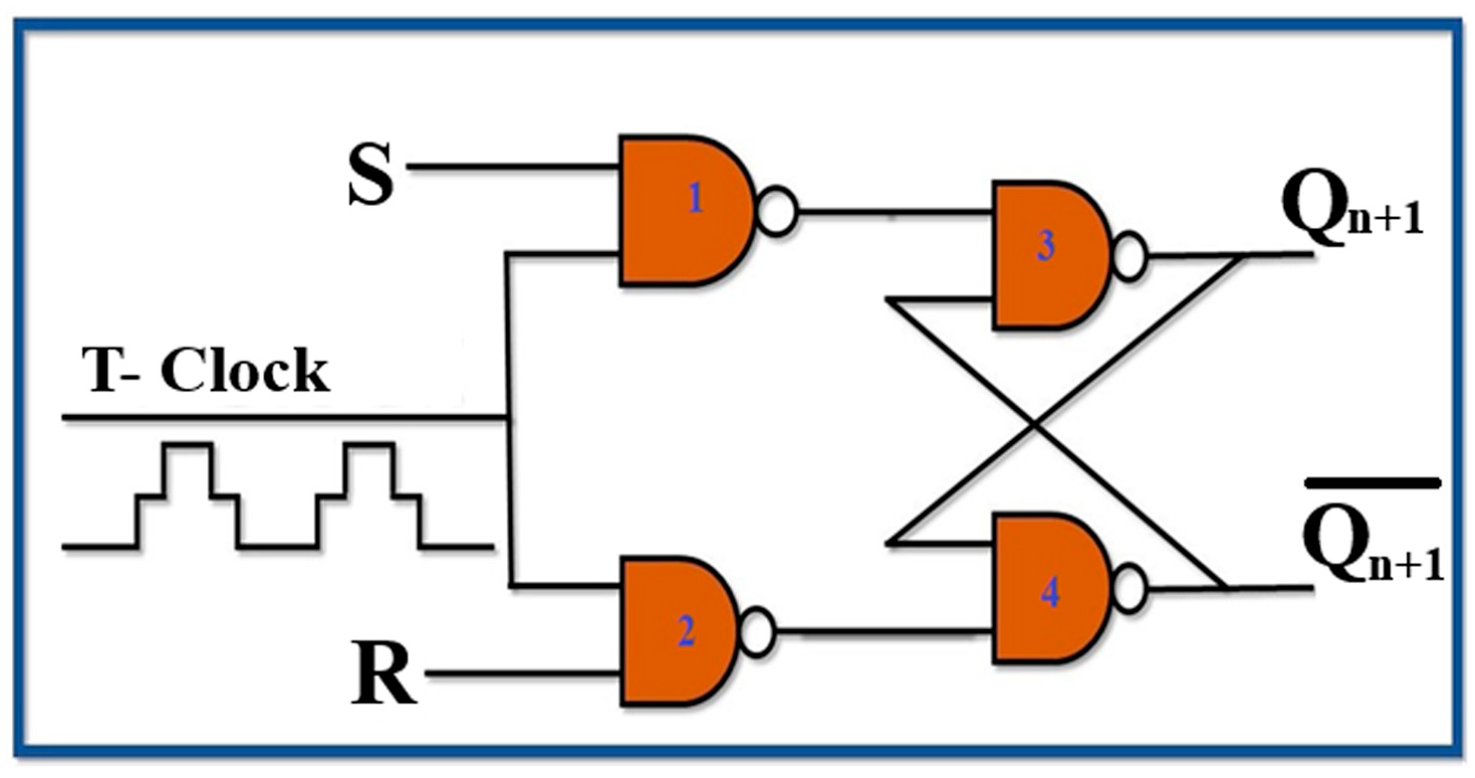
2. Theory of Ternary Inverter Circuit and Clocked SR Flip-Flop Circuit
- (a)
- 0: Horizontally polarized light or HPL (•);
- (b)
- 1: Linearly polarized light at 45° or L45P;
- (c)
- 2: Vertically polarized light or VPL (↑).
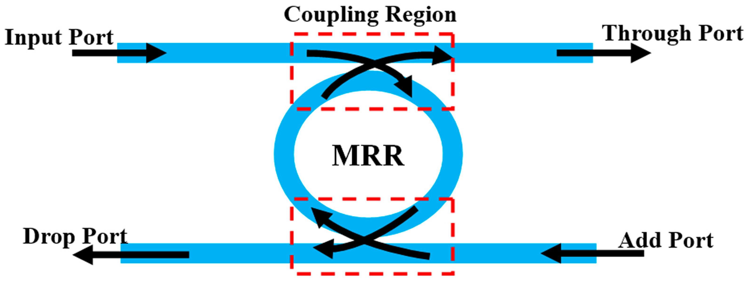
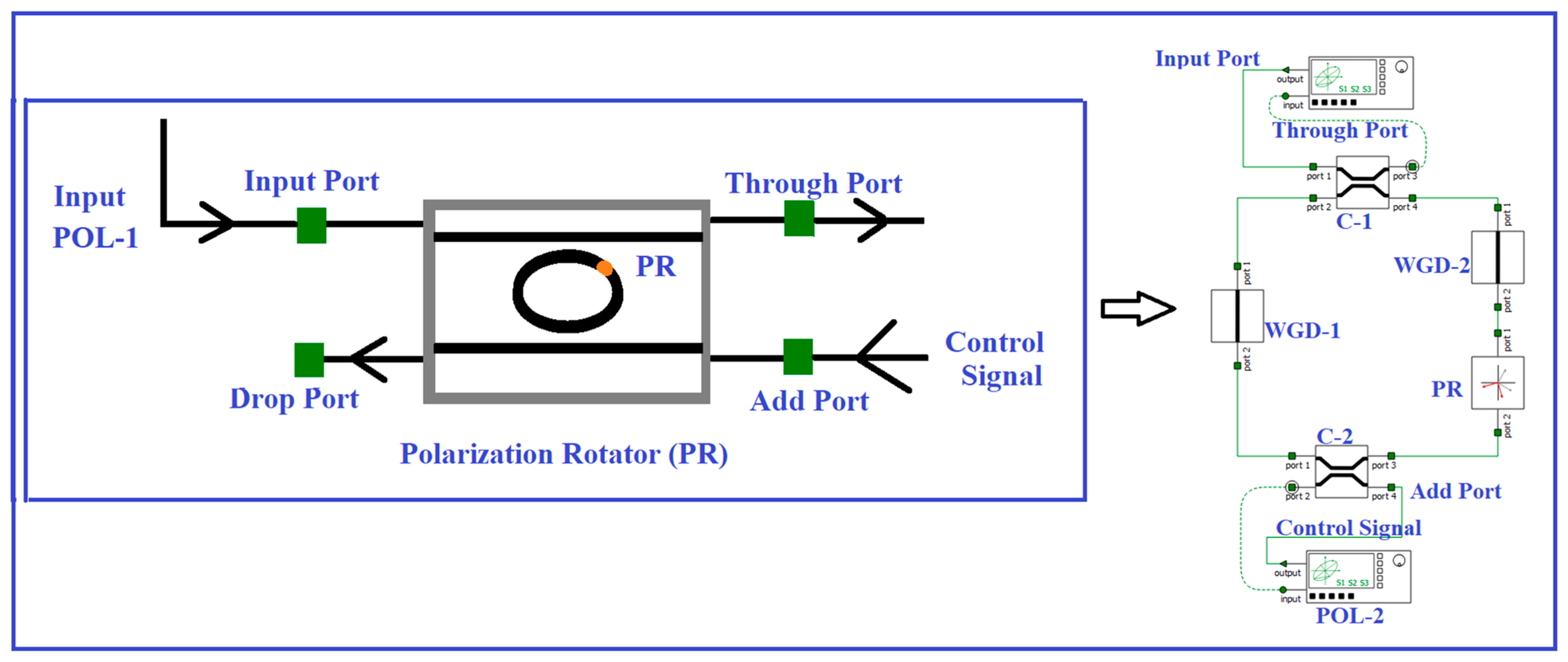
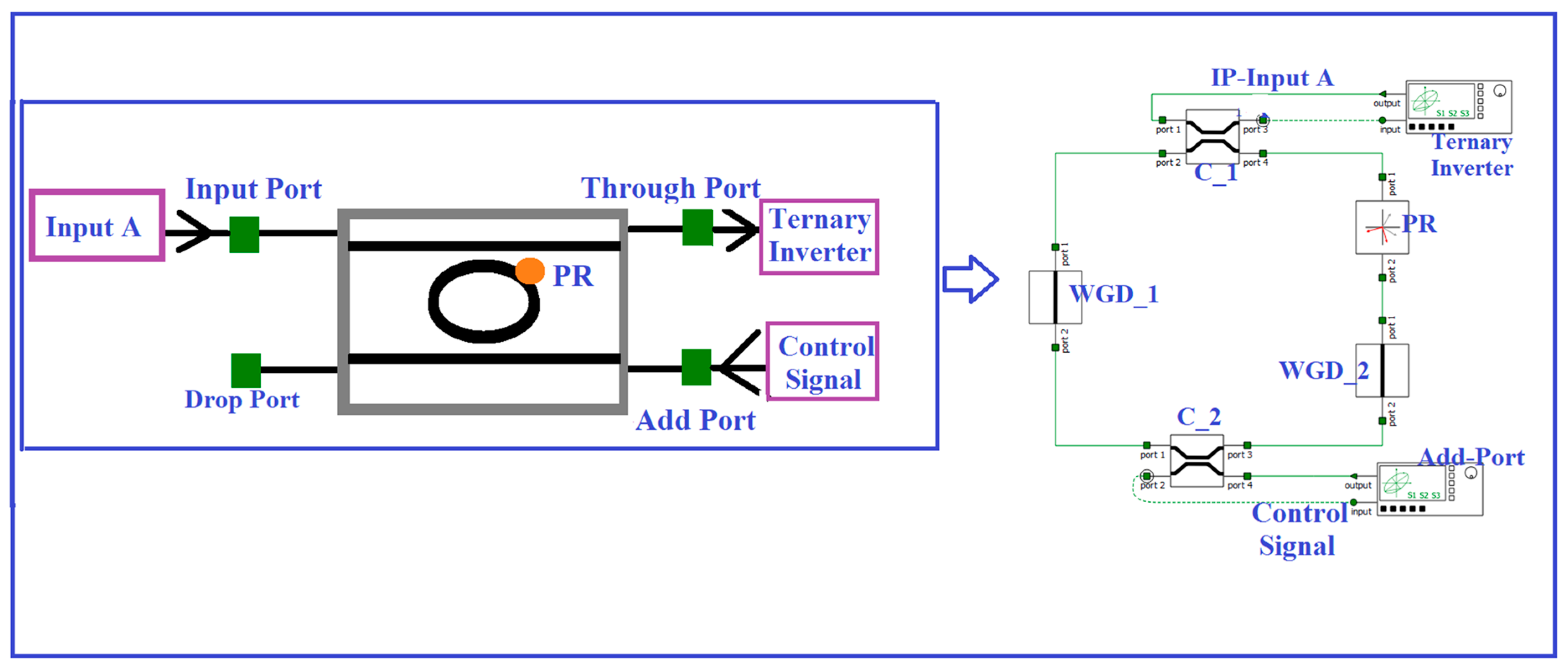
2.1. Modeling of MRR-Based Ternary Polarization Rotation Switch (PRS)
2.2. Ternary NAND Logic Gate Using MRR-PRS
3. Design of the Ternary Inverter and Clocked SR Flip-Flop Circuit
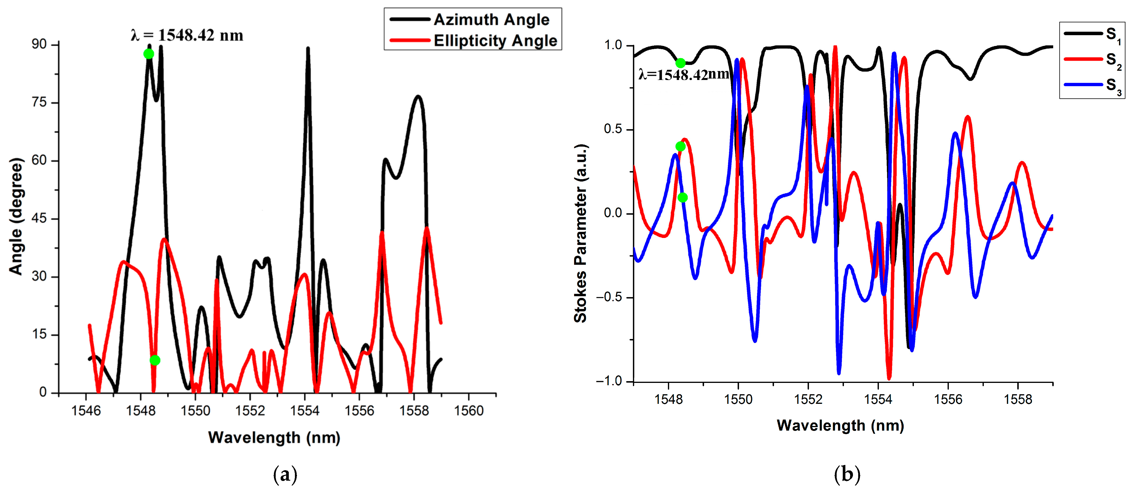
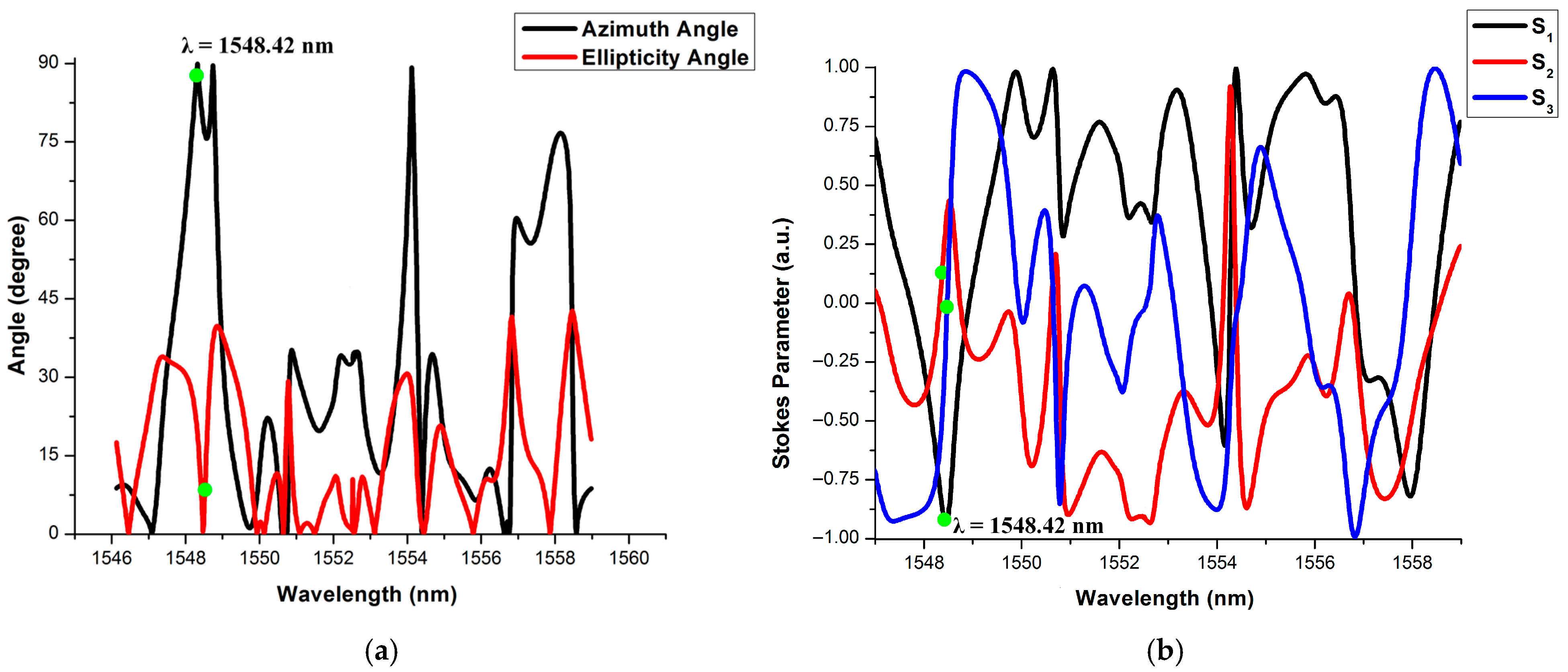
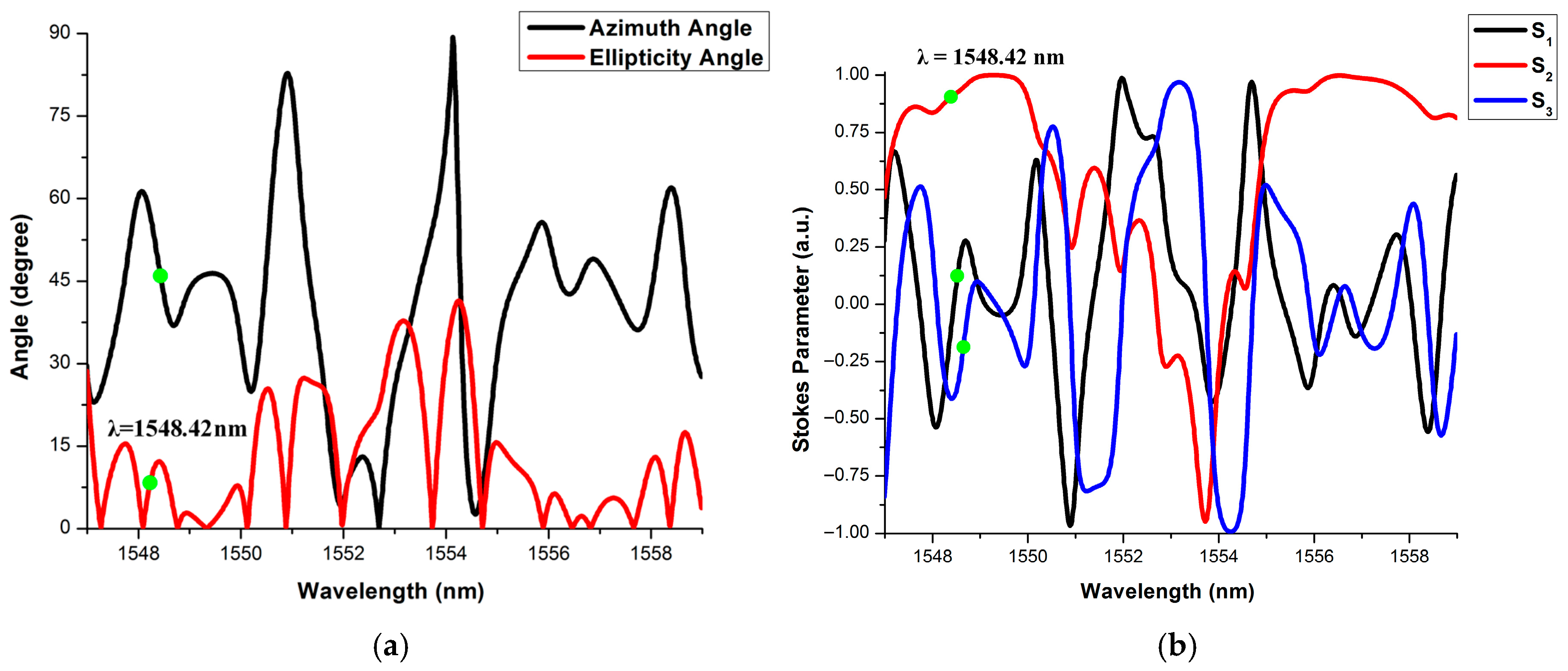
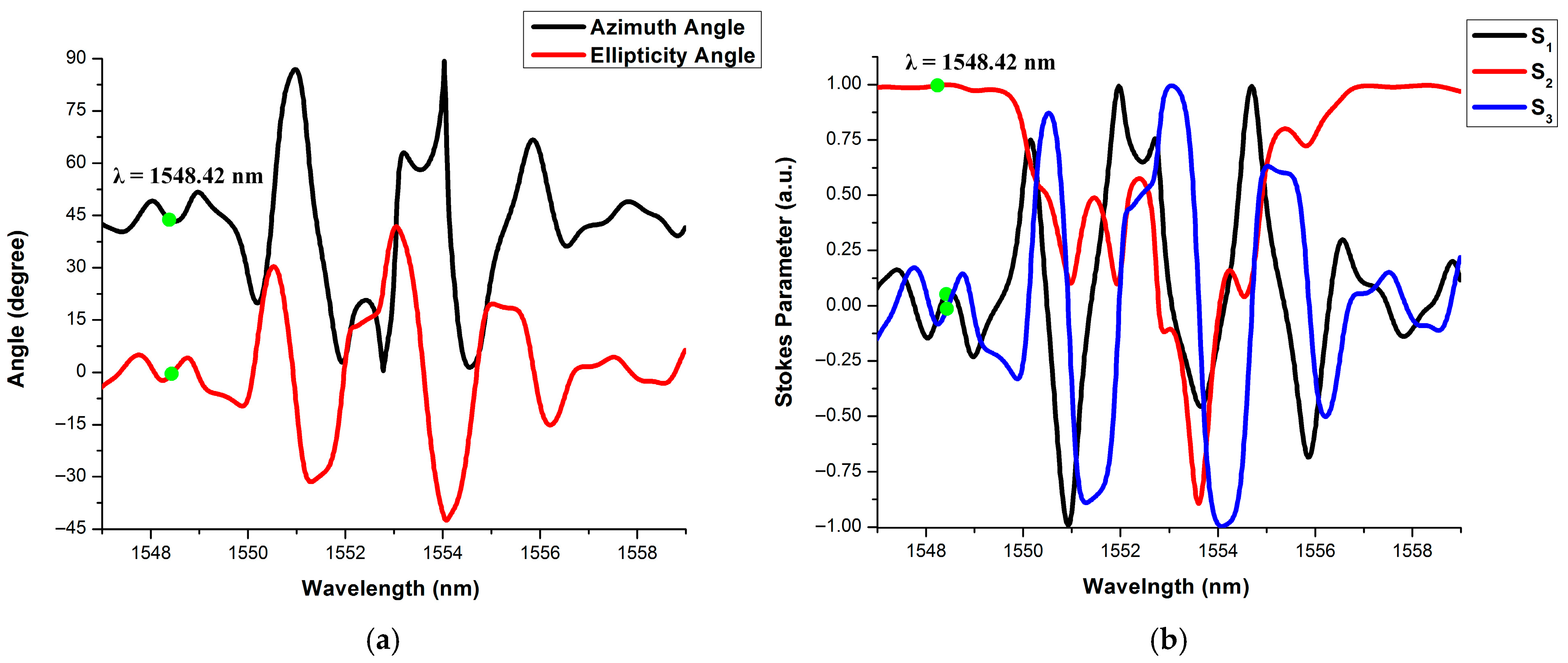
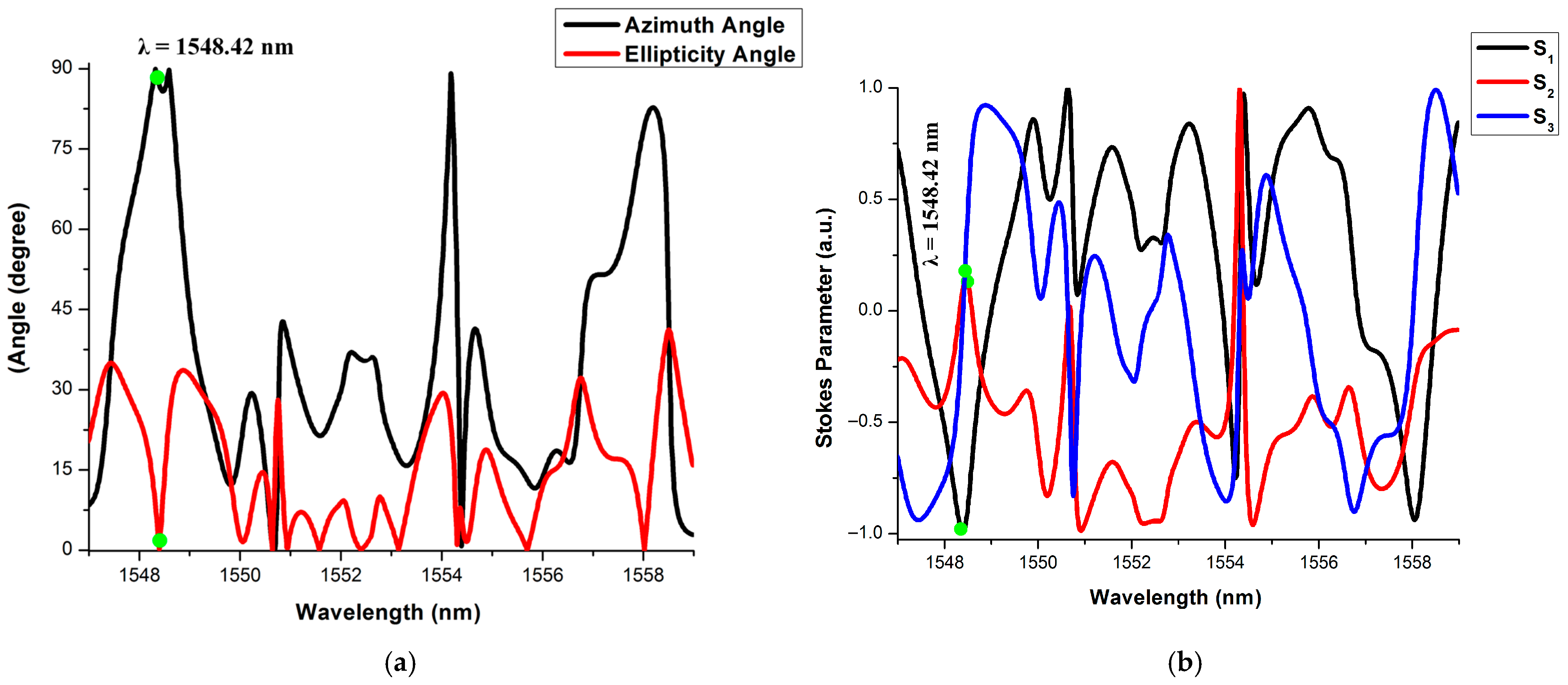
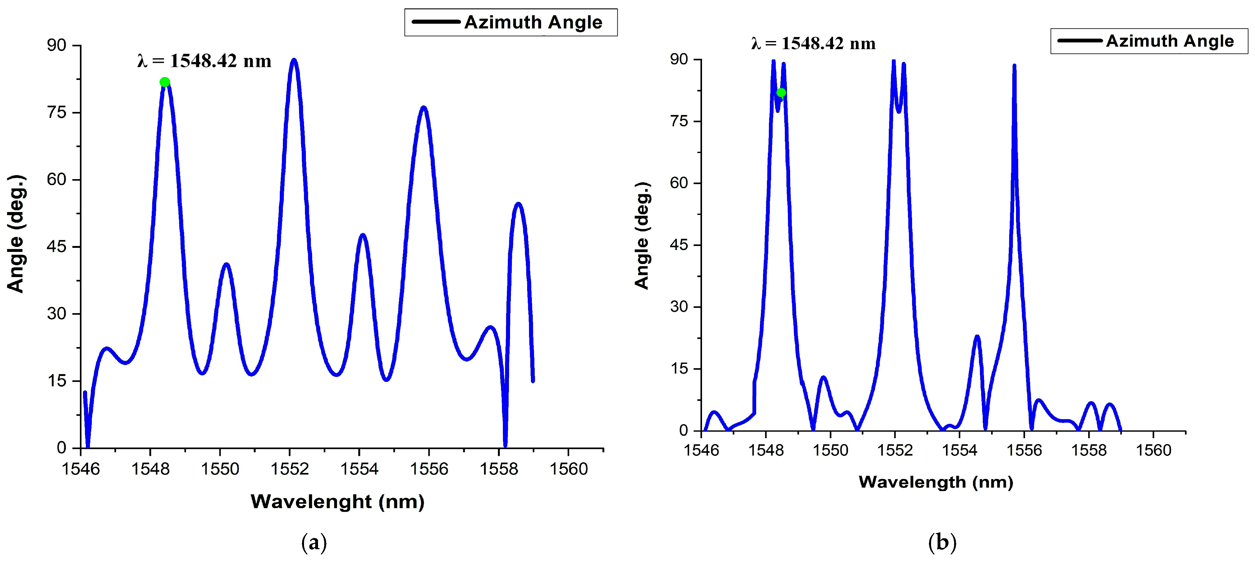
4. Simulation Results and Discussion
4.1. Inverter
4.2. Clocked SR Flip-Flop Circuit
4.3. Discussion
5. Conclusions
Author Contributions
Funding
Institutional Review Board Statement
Informed Consent Statement
Data Availability Statement
Conflicts of Interest
Abbreviations
| PRS | polarization rotation switch |
| TCSR | ternary clocked SR flip-flop |
| MRR | micro-ring resonator |
| AOS | All-optical switch |
| MZI | Mach-Zender Interferometer |
| TOAD | Terahertz Optical Asymmetrical Demultiplexer |
| OPNLM | Optical Nonlinear Material |
| MVL | multi-valued logic |
| DP | Drop Port |
| TP | Through Port |
| WGD | Waveguide |
| PR | polarization rotator |
| POL | polarization analyzer |
| TNAND | ternary NAND gate |
| HPL | Horizontally polarized light |
| L45P | Linearly polarized light at 45° |
| VPL | Vertically polarized light |
References
- Li, Z.; Chen, Z.; Li, B. Optical pulse controlled all-optical logic gates in SiGe/Si multimode interference. Opt. Express 2005, 13, 1033–1038. [Google Scholar] [CrossRef] [PubMed]
- Hossain, M.; Rakshit, J.K.; Singh, M.P. Numerical analysis of all-optical silicon microring resonator-based cyclic redundancy check encoder. J. Nanophoton. 2022, 16, 036007. [Google Scholar] [CrossRef]
- Rizou, Z.V.; Zoiros, K.E. Performance analysis and improvement of semiconductor optical amplifier direct modulation with assistance of microring resonator notch filter. Opt. Quantum Electron. 2017, 49, 119. [Google Scholar] [CrossRef]
- Rao, D.G.S.; Swarnakar, S.; Palacharla, V.; Raju, K.S.R.; Kumar, S. Design of all-optical AND, OR, and XOR logic gates using photonic crystals for switching applications. Photonic Netw. Commun. 2021, 41, 109–118. [Google Scholar] [CrossRef]
- Hossain, M.; Zoiros, K.E.; Chattopadhyay, T.; Rakshit, J.K. Speed enhancement of all-optical pseudo random binary sequence (PRBS) generator using microring resonator. Opt. Quantum Electron. 2021, 53, 670. [Google Scholar] [CrossRef]
- Rakshit, J.K.; Zoiros, K.E.; Bharti, G.K. Proposal for ultrafast all-optical pseudo random binary sequence generator using microring resonator-based switches. J. Comput. Electron. 2021, 20, 353–367. [Google Scholar] [CrossRef]
- Ding, Y.; Ou, H.; Xu, J.; Xiong, M.; An, Y.; Hu, H.; Galili, M.; Riesgo, A.L.; Seoane, J.; Yvind, K.; et al. Linear all-optical signal processing using silicon micro-ring resonators. Front. Optoelectron. 2016, 9, 362–376. [Google Scholar] [CrossRef]
- Awwal, A.A.S.; Karim, M.A.; Cherri, A.K. Polarization-encoded optical shadow-casting scheme: Design of multioutput trinary combinational logic units. Appl. Opt. 1987, 26, 4814–4818. [Google Scholar] [CrossRef]
- Mandal, S.; Mandal, D.; Mandal, M.K.; Garai, S.K. Design of optical quaternary adder and subtractor using polarization switching. J. Opt. 2018, 47, 332–350. [Google Scholar] [CrossRef]
- Yan, J.; Jin, Y.; Zuo, K. Decrease-radix design principle for carrying/borrowing free multi-valued and application in ternary optical computer. Sci. China Ser. F Inf. Sci. 2008, 51, 1415–1426. [Google Scholar] [CrossRef]
- Rakshit, J.K.; Singh, M.P.; Hossain, M.; Roy, J.N. Polarization rotation based all-optical ternary half-adder and full-adder: Design and analysis using micro-ring resonator. Opt. Quantum Electron. 2022, 54, 128. [Google Scholar] [CrossRef]
- Jahromi, H.D.; Binaie, A.; Zarifkar, A.; Sheikhi, M.H. A new structure for all-optical three-input XOR logic gate based on semiconductor optical amplifier mach–zehnder interferometer. Int. J. Mod. Phys. B 2014, 28, 1450052. [Google Scholar] [CrossRef]
- Hamedi, S.; Jahromi, H.D. Performance analysis of all-optical logical gate using artificial neural network. Expert Syst. Appl. 2021, 178, 115029. [Google Scholar] [CrossRef]
- Parandin, F.; Yahya, S.I.; Rezaeenia, M.; Askarian, A.; Roshani, S.; Roshani, S.; Ghadi, Y.Y.; Jamshidi, M.; Rezaee, S. A neural networks approach for designing compact all-optical photonic crystal based AND logic gate. J. Opt. Commun. 2025, 45, s2627–s2636. [Google Scholar] [CrossRef]
- Singh, M.P.; Hossain, M.; Rakshit, J.K.; Bharti, G.K.; Roy, J.N. Proposal for Polarization Rotation–Based Ultrafast All Optical Switch in Ring Resonator. Braz. J. Phys. 2021, 51, 1763–1774. [Google Scholar] [CrossRef]
- Raja, A.; Mukherjee, K.; Roy, J.N. Ultra-high-speed all-optical multivalued inverter using nonlinear polarization rotation in semiconductor optical amplifier. J. Opt. 2022, 51, 517–525. [Google Scholar] [CrossRef]
- Hurst, S.L. Multiple-valued logic—It’s status and it’s future. IEEE Trans. Comput. C 1984, 33, 1160–1179. [Google Scholar] [CrossRef]
- Smith, K.C. Multiple-valued logic—A tutorial and appreciation. IEEE Comput. 1988, 8, 17–27. [Google Scholar] [CrossRef]
- Cunha, R.; Boudinov, H.; Carro, L. Quaternary look-up tables using voltage mode CMOS logic design. In Proceedings of the 37th International Symposium of multiple-valued logic (ISMVL’07), Oslo, Norway, 13–16 May 2007; p. 56. [Google Scholar]
- Chattopadhyay, T.; Roy, J.N. Polarization encoded all optical quaternary successor with the help of SOA assisted Sagnac switch. Opt. Commun. 2011, 284, 2755–2762. [Google Scholar] [CrossRef]
- Yasuda, Y.; Tokuda, Y.; Zaima, S.; Pak, K.; Nakamura, T.; Yoshida, A. Realization of quaternary logic circuits by n-channel MOS devices. IEEE J. Solid-State Circuits 1986, 21, 162–168. [Google Scholar] [CrossRef]
- Chattopadhyay, T.; Roy, J.N. Polarization-encoded all-optical quaternary universal inverter and design of multivalued flip-flop. Opt. Eng. 2010, 49, 035201. [Google Scholar] [CrossRef]
- Imai, Y.; Ohtsuka, Y. Optical multiple-output and multiplevalued logic operation based on fringe shifting techniques using a spatial light modulator. Appl. Opt. 1987, 26, 274–277. [Google Scholar] [CrossRef] [PubMed]
- Rizvi, R.A.; Zaheer, K.; Zubairy, M.S. Implementation of trinary logic in polarization encoded shadow-casting scheme. Appl. Opt. 1991, 30, 936–942. [Google Scholar] [CrossRef] [PubMed]
- Chattopadhyay, T.; Bhowmik, P.; Roy, J.N. Polarization encoded optical N-valued inverter. J. Opt. Soc. Am. B 2012, 29, 2852–2860. [Google Scholar] [CrossRef]
- Raja, A.; Mukherjee, K.; Roy, J.N. Design of dual semiconductor optical amplifier structure based all-optical standard quaternary inverter and quaternary clocked SR flip-flop. Opt. Quantum Electron. 2022, 54, 39. [Google Scholar] [CrossRef]
- Chattopadhyay, T. All-optical symmetric ternary logic gate. Opt. Laser Technol. 2010, 42, 1014–1021. [Google Scholar] [CrossRef]
- Singh, M.P.; Rakshit, J.K.; Hossain, M. Implantation of polarization rotation based ternary 3:1 multiplexer and 1:3 demultiplexer using optical micro ring resonator. Opt. Commun. 2022, 522, 128646. [Google Scholar] [CrossRef]
- Singh, M.P.; Rakshit, J.K.; Hossain, M. Design of polarization conversion and rotation based ternary logic AND/NAND, OR/NOR, Ex-OR/Ex-NOR gates using ring resonator. Opt. Quantum Electron. 2021, 53, 703. [Google Scholar] [CrossRef]
- Chrostowski, L.; Lu, Z.; Flueckiger, J.; Wang, X.; Klein, J.; Liu, A.; Jhoja, J.; Pond, J.; Vivien, L.; Pavesi, L.; et al. Design and simulation of silicon photonic schematics and layouts. Silicon Photonics Photonic Integr. Circuits V 2016, 9891, 185–195. [Google Scholar]
- Li, J.; Li, L.; Jin, L.; Li, C. All-optical switch and limiter based on nonlinear polarization in Mach–Zehnder interferometer coupled with a polarization-maintaining fiber-ring resonator. Opt. Commun. 2006, 260, 318–323. [Google Scholar] [CrossRef]
- Singh, M.P.; Rakshit, J.K.; Hossain, M. Modeling of Polarization-Conversion and Rotation-Based Ultrafast All-Optical Ternary Logic Switch Using Microring Resonator. Braz. J. Phys. 2023, 53, 40. [Google Scholar] [CrossRef]
- Jahrom, H.D. Germanium-incorporated Si-Ge-Si heterojunction phototransistors for a high-limit of detection and wide linear dynamic range near-infrared light detection. Opt. Express 2024, 32, 43475–43489. [Google Scholar] [CrossRef]
- Jahromi, H.D.; Mahmoodi, A.; Sheikhi, M.H.; Zarifkar, A. Spectral response, dark current, and noise analyses in resonant tunneling quantum dot infrared photodetectors. Appl. Opt. 2016, 55, 8494–8499. [Google Scholar] [CrossRef]
- Jahromi, H.D.; Zarifkar, A. A physical model for quantum wire infrared photodetectors under illumination condition. Opt. Commun. 2021, 493, 127043. [Google Scholar] [CrossRef]
- Yang, T.; Liu, X.; Li, H.; Wang, C.; Sun, J.; Zhou, J. THz polarization conversion metamaterial based on bianisotropic response of split-ring resonators. J. Phys. D Appl. Phys. 2020, 53, 345102. [Google Scholar] [CrossRef]
- Bokhari, S.H.A.; Cheema, H.M. Broadband asymmetric transmission via angle-induced chirality enhancement in split ring resonators. J. Appl. Phys. 2020, 128, 063102. [Google Scholar] [CrossRef]
- Rabus, D.; Hamacher, M.; Troppenz, U.; Heidrich, H. Optical filters based on ring resonators with integrated semiconductor optical amplifiers in GaInAsP-InP. IEEE J. Sel. Top. Quantum Electron. 2003, 8, 1405–1411. [Google Scholar] [CrossRef]


| Sl. No. | References | Mechanism | Structures/No. of Switches Used | Performance Analysis | Advantages | Drawbacks |
|---|---|---|---|---|---|---|
| 1 | T. Chattopadhyay and J. N. Roy [22] | SOA-assisted Sagnac switch-based all-optical quaternary universal inverter. | 2 TOAD-based switches are used for inverters. | Power, 0.2 mW; switching time, not mentioned. | High-speed, simple optical control structure. | The main drawback of SOA-based AOSs is that it has speed limitations due to the relatively slow recovery of the carrier density in the amplifier’s active region. It has some problems with temperature variations and might have trouble keeping the signals polarized. |
| 2 | A. Raja, et al. [26] | Dual SOA-based all-optical quaternary inverter and clocked SR flip-flop. | 2 SOA-based switches are used for inverter. 24 SOA-based switches are used for flip-flop. Relatively complex in nature. | Power, 0.2 mW for single SOA; data rate, 333 Gbps. | High-speed, simple optical control structure. | The main drawback of SOA-based AOSs is that it has speed limitations due to the relatively slow recovery of the carrier density in the amplifier’s active region. It has some problems with temperature variations and might have trouble keeping the signals polarized. |
| 3 | T. Chattopadhyay [27] | TOAD-based ternary logic gates. | 2 TOAD-based interferometric switches for ternary MIN/MAX gate. | Power not mentioned; switching time not mentioned. | Normally high operational speed and low level of switching energy. | Normally, power consumption is high, wavelength selectivity is poor, and cascadability is difficult. |
| 4 | M. P. singh [28] | Ring resonator-based ternary multiplexer and demultiplexer circuit. | 3-micro-ring resonator-based ternary AND gate. | Power, 80 µW to 1.35 mW; switching time, 0.714 ps. | Ultra-compact, very high operational speed, high wavelength selectivity, low power consumption, and high integration capacity. | Fabrication-sensitive, and narrow bandwidth. |
| S. No. | Parameters | Description |
|---|---|---|
| I. | MRR waveguide material | GaAs |
| II. | Nature of coupling | Lateral coupling |
| III. | Coupling coefficient (k1, k2) | 0.45, 0.45 |
| IV. | Refractive index of GaAs | 3.38 |
| V. | Coupling length | 3 μm |
| VI. | MRR radius | 12 μm |
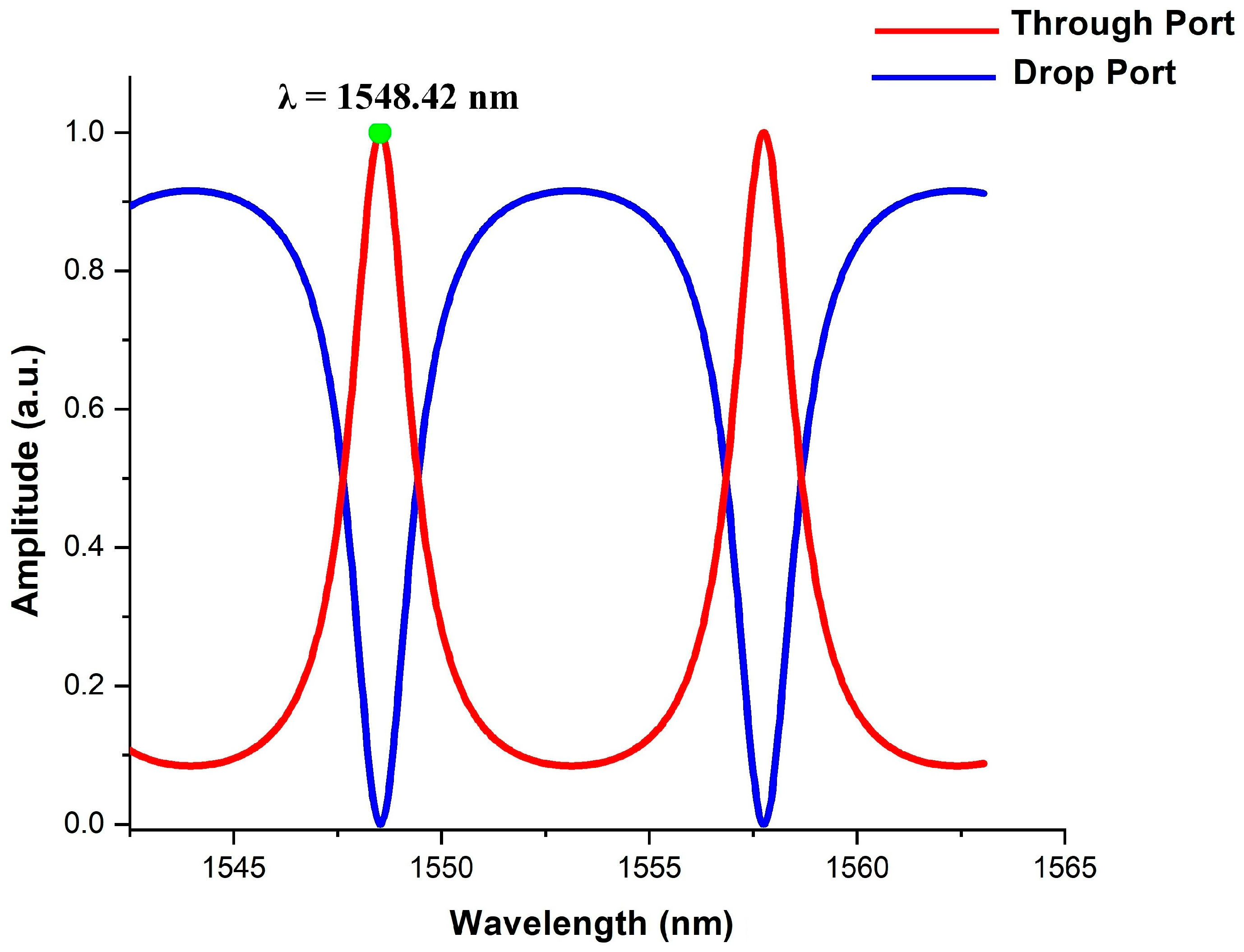
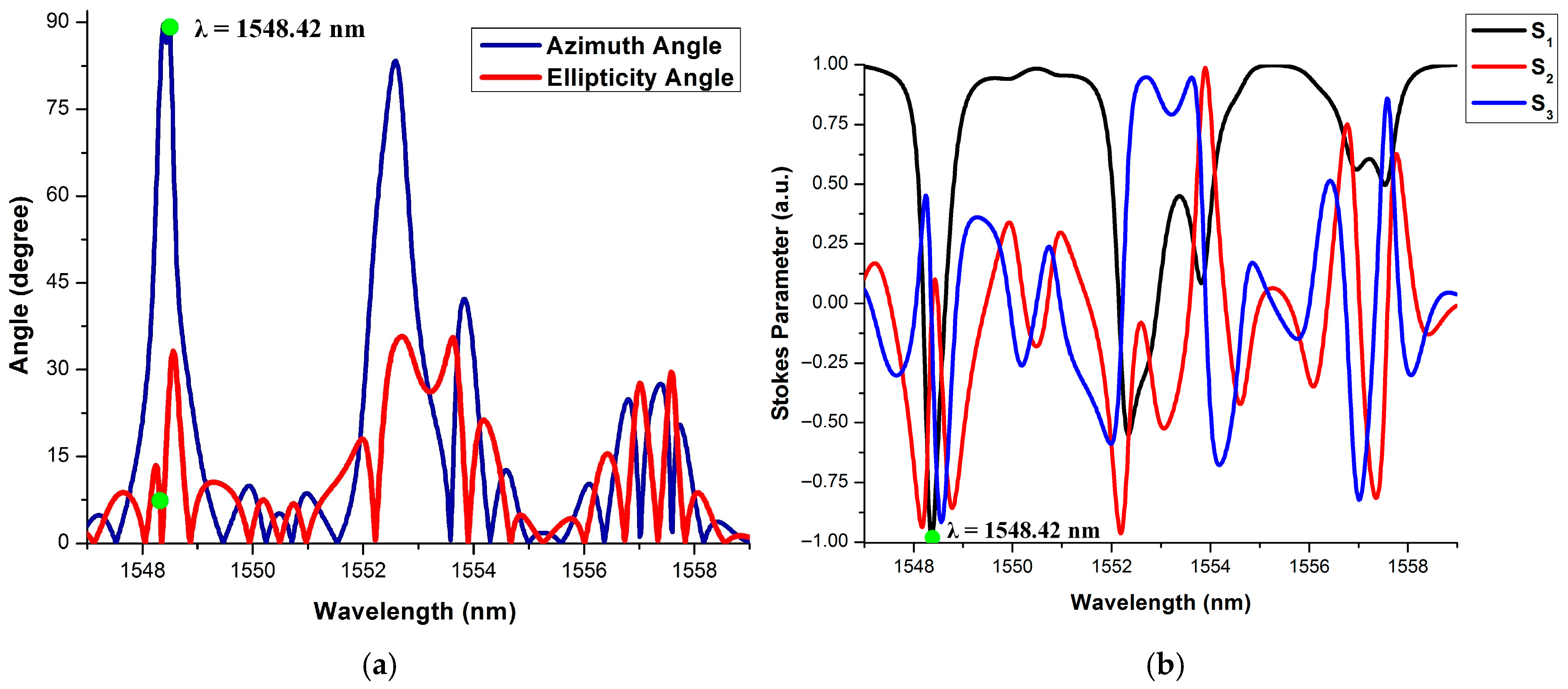
| VII. | Resonance wavelength | 1548.42 nm |
| VIII. | Polarization rotation angle | 60° |
| Input Port (A) | Add Port (B) | “Through Port” (NAND Gate) |
|---|---|---|
| HPL(‘Logic-0’) | HPL(‘Logic-0’) | VPL(‘Logic-2’) |
| L45P (‘Logic-1’) | HPL(‘Logic-0’) | VPL(‘Logic-2’) |
| VPL(‘Logic-2’) | HPL(‘Logic-0’) | VPL(‘Logic-2’) |
| HPL(‘Logic-0’) | L45P (‘Logic-1’) | VPL(‘Logic-2’) |
| L45P (‘Logic-1’) | L45P (‘Logic-1’) | L45P (‘Logic-1’) |
| VPL(‘Logic-2’) | L45P (‘Logic-1’) | L45P (‘Logic-1’) |
| HPL(‘Logic-0’) | VPL(‘Logic-2’) | VPL(‘Logic-2’) |
| L45P (‘Logic-1’) | VPL(‘Logic-2’) | L45P (‘Logic-1’) |
| VPL(‘Logic-2’) | VPL(‘Logic-2’) | HPL(‘Logic-0’) |
| Input Port (A) | Pump Source (B) | “Through Port” Output (NAND Gate) | ||
|---|---|---|---|---|
| Logic State | Pump Power | Azimuth Angle (E = 0°) | Output Polarization State | |
| HPL ‘Logic-0’ | HPL | 240 μW | 90° | VPL(‘Logic-2’) |
| L45P | 400 μW | 90° | VPL(‘Logic-2’) | |
| VPL | 915 μW | 90° | VPL(‘Logic-2’) | |
| L45P ‘Logic-1’ | HPL | 185 μW | 90° | VPL(‘Logic-2’) |
| L45P | 10 μW | 45° | L45P (‘Logic-1’) | |
| VPL | 18 μW | 45° | L45P (‘Logic-1’) | |
| VPL ‘Logic-2’ | HPL | 8 μW | 90° | VPL(‘Logic-2’) |
| L45P | 200 μW | 45° | L45P (‘Logic-1’) | |
| VPL | 380 μW | 0° | HPL(‘Logic-0’) | |
| Input Polarization States | Control Signal | Output Polarization States (Y) |
|---|---|---|
| HPL | HPL | HPL |
| L45P | ||
| VPL | ||
| L45P | HPL | |
| L45P | ||
| VPL | ||
| VPL | HPL | |
| L45P | ||
| VPL | ||
| L45P | HPL | HPL |
| L45P | ||
| VPL | ||
| L45P | HPL | |
| L45P | ||
| VPL | ||
| VPL | HPL | |
| L45P | ||
| VPL | ||
| VPL | HPL | HPL |
| L45P | ||
| VPL | ||
| L45P | HPL | |
| L45P | ||
| VPL | ||
| VPL | HPL | |
| L45P | ||
| VPL |
| Ternary Clock | Input-S | Input-R | Previous State | Next State | Remark | ||
|---|---|---|---|---|---|---|---|
| Qn | Qn+1 | ||||||
| ‘Logic-0’ (HPL) | ‘Logic-0’ | ‘Logic-0’ | ‘Logic-0’ | ‘Logic-2’ | 0 | 2 | Unchanged |
| ‘Logic-2’ | ‘Logic-0’ | 2 | 0 | Unchanged | |||
| ‘Logic-1’ | ‘Logic-1’ | 1 | 1 | Unchanged | |||
| ‘Logic-0’ | ‘Logic-1’ | ‘Logic-0’ | ‘Logic-2’ | 0 | 2 | Reset | |
| ‘Logic-2’ | ‘Logic-0’ | 2 | 0 | Set | |||
| ‘Logic-1’ | ‘Logic-1’ | 1 | 1 | Intermediate | |||
| ‘Logic-0’ | ‘Logic-2’ | ‘Logic-0’ | ‘Logic-2’ | 0 | 2 | Reset | |
| ‘Logic-2’ | ‘Logic-0’ | 2 | 0 | Set | |||
| ‘Logic-1’ | ‘Logic-1’ | 1 | 1 | Intermediate | |||
| ‘Logic-1’ (L45P) | ‘Logic-1’ | ‘Logic-0’ | ‘Logic-0’ | ‘Logic-2’ | 1 | 2 | Forbidden |
| ‘Logic-2’ | ‘Logic-0’ | 2 | 1 | Forbidden | |||
| ‘Logic-1’ | ‘Logic-1’ | 1 | 1 | Intermediate | |||
| ‘Logic-1’ | ‘Logic-1’ | ‘Logic-0’ | ‘Logic-2’ | 1 | 2 | Forbidden | |
| ‘Logic-2’ | ‘Logic-0’ | 2 | 1 | Forbidden | |||
| ‘Logic-1’ | ‘Logic-1’ | 1 | 1 | Intermediate | |||
| ‘Logic-1’ | ‘Logic-2’ | ‘Logic-0’ | ‘Logic-2’ | 1 | 2 | Forbidden | |
| ‘Logic-2’ | ‘Logic-0’ | 2 | 1 | Forbidden | |||
| ‘Logic-1’ | ‘Logic-1’ | 1 | 1 | Intermediate | |||
| ‘Logic-2’ (VPL) | ‘Logic-2’ | ‘Logic-0’ | ‘Logic-0’ | ‘Logic-2’ | 0 | 2 | Reset |
| ‘Logic-2’ | ‘Logic-0’ | 2 | 0 | Set | |||
| ‘Logic-1’ | ‘Logic-1’ | 1 | 1 | Intermediate | |||
| ‘Logic-2’ | ‘Logic-1’ | ‘Logic-0’ | ‘Logic-2’ | 2 | 2 | Forbidden | |
| ‘Logic-2’ | ‘Logic-0’ | 2 | 1 | Forbidden | |||
| ‘Logic-1’ | ‘Logic-1’ | 1 | 1 | Intermediate | |||
| ‘Logic-2’ | ‘Logic-2’ | ‘Logic-0’ | ‘Logic-2’ | 2 | 2 | Forbidden | |
| ‘Logic-2’ | ‘Logic-0’ | 2 | 2 | Forbidden | |||
| ‘Logic-1’ | ‘Logic-1’ | 2 | 2 | Forbidden | |||
| Input Port Polarization State | Add-Port Polarization State | Control Signal Power | Output | Through Port “Polarization State” | |
|---|---|---|---|---|---|
| (Az, E), | (S1, S2, S3) | ||||
| Logic-0 (HPL) | Logic-0 (HPL) | 10 μW | (0°, 0°) | (1, 0, 0) | Logic-0 (HPL) |
| 90 μW | (45°, 0°) | (−1, 0, 0) | Logic-1 (L45P) | ||
| 180 μW | (90°, 0°) | (0, 1, 0) | Logic-2 (VPL) | ||
| Logic-0 (HPL) | Logic-1 (L45P) | 20 μW | (0°, 0°) | (1, 0, 0) | Logic-0 (HPL) |
| 950 μW | (45°, 0°) | (−1, 0, 0) | Logic-1 (L45P) | ||
| 880 μW | (90°, 0°) | (0, 1, 0) | Logic-2 (VPL) | ||
| Logic-0 (HPL) | Logic-2 (VPL) | 10 μW | (0°, 0°) | (1, 0, 0) | Logic-0 (HPL) |
| 740 μW | (45°, 0°) | (−1, 0, 0) | Logic-1 (L45P) | ||
| 965 μW | (90°, 0°) | (0, 1, 0) | Logic-2 (VPL) | ||
| Logic-1 (L45P) | Logic-0 (HPL) | 165 μW | (0°, 0°) | (1, 0, 0) | Logic-0 (HPL) |
| 15 μW | (45°, 0°) | (−1, 0, 0) | Logic-1 (L45P) | ||
| 922 μW | (90°, 0°) | (0, 1, 0) | Logic-2 (VPL) | ||
| Logic-1 (L45P) | Logic-1 (L45P) | 10 μW | (0°, 0°) | (1, 0, 0) | Logic-0 (HPL) |
| 650 μW | (45°, 0°) | (−1, 0, 0) | Logic-1 (L45P) | ||
| 867 μW | (90°, 0°) | (0, 1, 0) | Logic-2 (VPL) | ||
| Logic-1 (L45P) | Logic-2 (VPL) | 114 μW | (0°, 0°) | (1, 0, 0) | Logic-0 (HPL) |
| 990 μW | (45°, 0°) | (−1, 0, 0) | Logic-1 (L45P) | ||
| 10 μW | (90°, 0°) | (0, 1, 0) | Logic-2 (VPL) | ||
| Logic-2 (VPL) | Logic-0 (HPL) | 915 μW | (0°, 0°) | (1, 0, 0) | Logic-0 (HPL) |
| 650 μW | (45°, 0°) | (−1, 0, 0) | Logic-1 (L45P) | ||
| 14 μW | (90°, 0°) | (0, 1, 0) | Logic-2 (VPL) | ||
| Logic-2 (VPL) | Logic-1 (L45P) | 450 μW | (0°, 0°) | (1, 0, 0) | Logic-0 (HPL) |
| 910 μW | (45°, 0°) | (−1, 0, 0) | Logic-1 (L45P) | ||
| 10 μW | (90°, 0°) | (0, 1, 0) | Logic-2 (VPL) | ||
| Logic-2 (VPL) | Logic-2 (VPL) | 480 μW | (0°, 0°) | (1, 0, 0) | Logic-0 (HPL) |
| 910 μW | (45°, 0°) | (−1, 0, 0) | Logic-1 (L45P) | ||
| 10 μW | (90°, 0°) | (0, 1, 0) | Logic-2 (VPL) | ||
| T-Clock | Input S | Input R | Control Signal Power, CS-1 | Control Signal Power, CS-2 | Qn | Qn+1 | Remarks | ||
|---|---|---|---|---|---|---|---|---|---|
| Active State (HPL) | 0 | 0 | 12 μW | 160 μW | 0 | 2 | 0 | 2 | Unchanged |
| 0 | 0 | 75 μW | 15 μW | 2 | 0 | 2 | 0 | Unchanged | |
| 0 | 0 | 670 μW | 670 μW | 1 | 1 | 1 | 1 | Unchanged | |
| 0 | 1 | 340 μW | 880 μW | 0 | 2 | 0 | 2 | Reset | |
| 0 | 1 | 1.02 mW | 1.10 mW | 2 | 0 | 2 | 0 | Set | |
| 0 | 1 | 170 μW | 170 μW | 1 | 1 | 1 | 1 | Intermediate | |
| 0 | 2 | 85 μW | 140 μW | 0 | 2 | 0 | 2 | Reset | |
| 0 | 2 | 640 μW | 1.40 mW | 2 | 0 | 2 | 0 | Set | |
| 0 | 2 | 810 μW | 320 μW | 1 | 1 | 1 | 1 | Forbidden | |
| Active State (L45L) | 1 | 0 | 1.02 mW | 140 μW | 0 | 2 | 1 | 2 | Forbidden |
| 1 | 0 | 850 μW | 955 μW | 2 | 0 | 2 | 1 | Forbidden | |
| 1 | 0 | 170 μW | 170 μW | 1 | 1 | 1 | 1 | Intermediate | |
| 1 | 1 | 140 μW | 140 μW | 0 | 2 | 1 | 2 | Forbidden | |
| 1 | 1 | 35 μW | 155 μW | 2 | 0 | 2 | 1 | Forbidden | |
| 1 | 1 | 170 μW | 270 μW | 1 | 1 | 1 | 1 | Intermediate | |
| 1 | 2 | 385 μW | 1.15 mW | 0 | 2 | 1 | 2 | Forbidden | |
| 1 | 2 | 140 μW | 140 μW | 2 | 0 | 2 | 1 | Forbidden | |
| 1 | 2 | 560 μW | 440 μW | 1 | 1 | 1 | 1 | Intermediate | |
| Active State (VPL) | 2 | 0 | 1.50 mW | 1.02 mW | 0 | 2 | 0 | 2 | Reset |
| 2 | 0 | 850 μW | 850 μW | 2 | 0 | 2 | 0 | Set | |
| 2 | 0 | 170 μW | 240 μW | 1 | 1 | 1 | 1 | Forbidden | |
| 2 | 1 | 140 μW | 180 μW | 0 | 2 | 2 | 2 | Forbidden | |
| 2 | 1 | 155 μW | 120 μW | 2 | 0 | 2 | 1 | Forbidden | |
| 2 | 1 | 670 μW | 445 μW | 1 | 1 | 1 | 1 | Intermediate | |
| 2 | 2 | 385 µW | 140 μW | 0 | 2 | 2 | 2 | Forbidden | |
| 2 | 2 | 470 μW | 810 μW | 2 | 0 | 2 | 2 | Forbidden | |
| 2 | 2 | 540 μW | 1.24 mW | 1 | 1 | 2 | 2 | Forbidden |
Disclaimer/Publisher’s Note: The statements, opinions and data contained in all publications are solely those of the individual author(s) and contributor(s) and not of MDPI and/or the editor(s). MDPI and/or the editor(s) disclaim responsibility for any injury to people or property resulting from any ideas, methods, instructions or products referred to in the content. |
© 2025 by the authors. Licensee MDPI, Basel, Switzerland. This article is an open access article distributed under the terms and conditions of the Creative Commons Attribution (CC BY) license (https://creativecommons.org/licenses/by/4.0/).
Share and Cite
Singh, M.P.; Rakshit, J.K.; Zoiros, K.E.; Hossain, M. Design of All-Optical Ternary Inverter and Clocked SR Flip-Flop Based on Polarization Conversion and Rotation in Micro-Ring Resonator. Photonics 2025, 12, 762. https://doi.org/10.3390/photonics12080762
Singh MP, Rakshit JK, Zoiros KE, Hossain M. Design of All-Optical Ternary Inverter and Clocked SR Flip-Flop Based on Polarization Conversion and Rotation in Micro-Ring Resonator. Photonics. 2025; 12(8):762. https://doi.org/10.3390/photonics12080762
Chicago/Turabian StyleSingh, Madan Pal, Jayanta Kumar Rakshit, Kyriakos E. Zoiros, and Manjur Hossain. 2025. "Design of All-Optical Ternary Inverter and Clocked SR Flip-Flop Based on Polarization Conversion and Rotation in Micro-Ring Resonator" Photonics 12, no. 8: 762. https://doi.org/10.3390/photonics12080762
APA StyleSingh, M. P., Rakshit, J. K., Zoiros, K. E., & Hossain, M. (2025). Design of All-Optical Ternary Inverter and Clocked SR Flip-Flop Based on Polarization Conversion and Rotation in Micro-Ring Resonator. Photonics, 12(8), 762. https://doi.org/10.3390/photonics12080762