Abstract
An optical power splitter (OPS) with arbitrary splitting ratios has attracted significant research interest for its broad applications in photonic integrated circuits. A series of OPSs with arbitrary splitting ratios based on silicon nitride (Si3N4) platforms are presented. The devices are designed with ultra-compact dimensions using three-dimensional finite-difference time-domain (3D FDTD) analysis and an inverse design algorithm. Within a 50 nm bandwidth (1525 nm to 1575 nm), we demonstrated a 1 × 2 OPS with splitting ratios of 1:1, 1:1.5, and 1:2; a 1 × 3 OPS with ratios of 1:2:1 and 2:1:2; and a 1 × 4 OPS with ratios of 1:1:1:1 and 2:1:2:1. The target splitting ratios are achieved by optimizing pixel distributions in the coupling region. The dimensions of the designed devices are 1.96 × 1.96 µm2, 2.8 × 2.8 µm2, and 2.8 × 4.2 µm2, respectively. The designed devices achieve transmission efficiencies exceeding 90% and exhibit excellent power splitting ratios (PSRs).
1. Introduction
In recent years, the rapid advancement of communication technology has increasingly highlighted the physical limitations of electronic integrated circuits (EICs) [1]. In contrast, photonic integrated circuits (PICs) overcome these limitations and provide high transmission rates and broad bandwidths, resulting in extensive utilization. As fundamental components in nanophotonic systems, optical power splitters (OPSs) are widely utilized in various applications, including signal detection, signal feedback [2,3], and wavelength-division multiplexing systems [4]. OPSs provide reasonable power configurations and are integrated with other optical devices to fulfill diverse functional requirements. The design approaches for OPSs are mainly divided into the following two types: forward design method and inverse design method. The device structures based on the forward design are deduced from optical theories and practical experience [5]. Currently, the power splitter structures based on forward design have been reported, including asymmetric multimode interference (MMI) couplers [6], directional couplers (DCs) [7], Y-branches [8], and adiabatic couplers (ACs) [9,10,11]. Although these power splitters exhibit excellent performance, they are designed with an uncompact size, which hinders further integration. For example, Yanmei Lin et al. proposed and experimentally verified several 1 × 2 OPSs with power splitting ratios (PSRs) ranging from 50:50 to 5:95 using a thin-film lithium niobate platform [12]. The different splitting ratios were achieved by adjusting the geometry of the MMI region. All devices exhibit insertion losses below 0.3 dB at 1550 nm, with PSR variations under 3% over the 1520–1590 nm wavelength band. The coupling region length ranges from 57.5 µm to 108 µm. Shasha Liao et al. proposed and demonstrated an integrated OPS based on silicon-on-insulator [13]. The design integrates several common structures, including 2 × 2 multimode interferometric coupler, waveguide grating, and slot. The PSR can be continuously tuned by adjusting the input signal wavelength or the voltage applied to the on-chip electrodes. The coupling region length is approximately 56.5 µm.
To address the requirements of photonic system integration, the inverse design method has received increasing attention in recent years. Compared to forward design, inverse design maximizes the design space by utilizing an objective function to adjust discretized pixels, thereby altering the PSR and field distribution. The designed OPSs using this approach exhibit ultra-compact dimensions. The algorithms for inverse design include genetic algorithm [14], direct binary search (DBS) algorithm [15,16,17,18], particle swarm optimization (PSO) algorithm [19,20], and deep learning [21,22]. Recently, different ultra-compact OPSs based on inverse design have been reported. Ke Xu et al. proposed an ultra-compact power splitter design featuring QR code-like nanostructures [23], utilizing a nonlinear fast search method. A 1 × 2 splitter with PSRs of 1:1, 1:2, and 1:3, and a 1 × 3 splitter with a 1:2:1 splitting ratio, were demonstrated. All devices exhibit a compact footprint of 3.6 × 3.6 µm2, with measured transmission efficiencies approaching 80% across a 30 nm wavelength range. Yingjie Liu et al. experimentally demonstrated a polarization-insensitive MMI coupler with a footprint of 2.4 µm × 2.4 µm [24]. The device exhibited transmission efficiencies exceeding 90% for both TE and TM polarizations across the wavelength range of 1480 nm to 1560 nm. Hucheng Xie et al. designed a 1 × 4 power splitter on a silicon platform, supporting arbitrary PSRs across a 2 µm spectral range [25]. The device achieves transmission efficiency exceeding 80% and demonstrates excellent power ratio performance. Chong Meng et al. designed a 1 × 3 power splitter using inverse design, with a compact size of 2.8 × 2.8 µm2 and a splitting ratio of 25%:50%:25% [26]. In the 1500–1600 nm operation range, the device exhibits an insertion loss below 0.49 dB and a ratio variation under 4.4%.
In this study, we proposed a series of OPSs with arbitrary splitting ratios based on the silicon nitride (Si3N4) platforms and verified that the design method can be effectively extended to the design of multi-channel optical splitters. Due to the relatively low refractive index contrast, Si3N4 waveguides provide excellent performance with respect to minimizing optical losses and enhancing fabrication tolerance in both lithography and etching. The coupling region is discretized into small pixels, which are digitally optimized using the DBS algorithm. The target PSR is achieved by adjusting the pixel distribution. The designed 1 × 2 power splitter with splitting ratios of 1:1, 1:1.5, and 1:2 exhibits excellent performance across the 1525 nm to 1575 nm wavelength range. To verify the scalability of this design method for multi-channel configurations, 1 × 3 splitters with ratios of 1:2:1 and 2:1:2 and 1 × 4 splitters with ratios of 1:1:1:1 and 2:1:2:1 are investigated. The designed devices are ultra-compact with dimensions of 1.96 × 1.96 µm2, 2.8 × 2.8 µm2, and 2.8 × 4.2 µm2, respectively. All designed devices exhibit transmission efficiencies exceeding 90% and excellent splitting ratios.
2. Operating Principle and Simulation Results
The geometry (3D) of the designed 1 × 2 OPS with an adjustable splitting ratio is shown in Figure 1a. The device consists of three components: the input waveguide, the 1 × 2 MMI design area, and the output waveguides. By launching the fundamental transverse electric (TE0) mode into the device, the predefined power splitting ratio (PSR) is achieved at the output ports. All designed devices operate exclusively in TE0 mode. The output waveguides are axisymmetrically distributed strip waveguides. The waveguide layer consists of 800 nm-thick Si3N4, supported by a 2 µm-thick silicon dioxide (SiO2) substrate, beneath which lies a 200 nm-thick silicon (Si) layer. At a wavelength of 1550 nm, the effective refractive indices of Si3N4, SiO2, and Si are 2.462, 1.444, and 3.421, respectively. The device is encapsulated with a SiO2 upper cladding layer for structural protection. To ensure effective optical signal propagation, the input waveguide dimensions of the OPS must support single-mode transmission. Accordingly, both the input and output waveguides are designed with widths and heights of 800 nm. The output waveguides of the 1 × 2 power splitter are spaced 200 nm apart. Serving as a transition between the input and output waveguides, the MMI region is designed with an ultra-compact footprint of 1.96 × 1.96 µm2. For fabrication robustness, the region is uniformly discretized into 196 (14 × 14) square pixels, each with dimensions of 140 × 140 nm2. A circular hole with a diameter of 120 nm and a height of 800 nm is etched at the center of each pixel. As shown in Figure 1a, each circular hole occupies two states, where the blue regions represent Si3N4 state while the gray regions represent air state. The state distribution of the circular hole is automatically optimized using an algorithm, which adjusts the refractive index distribution in the MMI region to achieve optimal device performance. TE0 mode light propagates from the input waveguide to the MMI coupling region, and a monitor at the output waveguides measures the output power. Different from traditional MMI structure devices, this design maximizes the use of free space within the coupling region to control optical field distribution and power transmission, achieving an ultra-compact size and excellent performance. Additionally, the design enables fabrication in a single lithographic step and is compatible with CMOS fabrication processes.
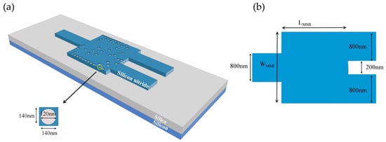
Figure 1.
(a) The geometry (3D) of the 1 × 2 optical power splitter (OPS); (b) the initial structure of the inverse-optimized 1 × 2 OPS.
The initial structure of the inverse-optimized device is designed using forward design methods, as illustrated in Figure 1b. To ensure reliable optical signal transmission over long distances, the input waveguide dimensions must satisfy single-mode transmission standards. Using the effective refractive index method, the input waveguide dimensions are set to 800 nm in both height and width. The dimensions of the MMI region were determined using the eigenmode expansion (EME) solver implemented in Mode Solutions software (Lumerical 2020 R2). Based on calculations, the MMI region dimensions were set to WMMI = 1.96 µm and LMMI = 1.96 µm. This high-quality initial structure improves the convergence speed and optimization efficiency of the inverse design process, leading to enhanced performance of the optimized device. Next, the initial structure was modeled in the FDTD Solutions software (Lumerical 2020 R2), including a simulated light source (TE0 mode) and a monitoring region. Subsequently, the script was executed, and the device structure was optimized using the FDTD Solutions programming interface of Python (PyCharm 2023.3.5). The DBS algorithm was employed in this work for inverse design, owing to its simplicity of implementation and rapid convergence.
In this work, the pixel states in the MMI design region are encoded as “0” and “1” to precisely track the states of all pixels in the computational model. The pixel state distribution is optimized using the DBS algorithm to determine the optimal refractive index configuration in the MMI region, thereby achieving the functional requirements. Specifically, “0” represents the un-etched state (Si3N4 state), while “1” represents the etched state (air state). It is worth noting that the DBS algorithm exhibits high sensitivity to the initial state distribution of the device during the optimization process. Therefore, a random pattern and a manually designed pattern were employed to optimize the devices, respectively. Figure 2 shows the optimization results, demonstrating that the device with a manually designed pattern achieves lower loss. To ensure high optimization efficiency, we employ manually designed initial patterns with all pixels in the MMI region set to “0”. Additionally, figure-of-merit (FOM) was employed as the objective function for inverse optimization. The optimization process is illustrated in Figure 3. During device optimization, the TE0 mode light was launched into the input waveguide. The optical power at the output ports was measured in the monitoring region and the data was transferred to the scripting program to calculate FOM, which evaluates the efficiency of device performance improvement. Specifically, the initial structure for the inverse design process is configured with all pixels set to the “0” state. A pixel is then randomly selected in the MMI region, and the electromagnetic equations are solved to compute the FOM. The selected pixel state is then flipped, and the FOM is recalculated. If the FOM value improves, the target device performance is enhanced and the pixel state is retained; otherwise, the pixel state is reverted to its previous state. After computing one pixel, the next pixel is randomly selected to solve the electromagnetic equations and calculate the FOM. The pixel state is then flipped, and the FOM is recalculated and compared. Once all pixel states in the MMI region have been traversed the first iteration is completed and the next iteration begins. The process continues until the FOM value reaches the target threshold or plateau. At this point, the resulting pixel state distribution corresponds to the optimal device performance.
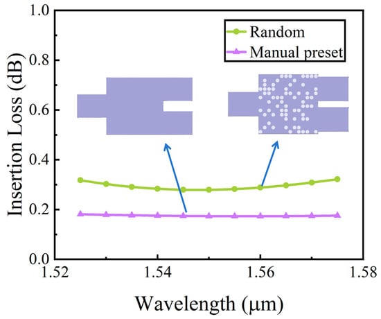
Figure 2.
Insertion losses for different initial structures.
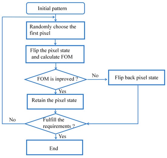
Figure 3.
Algorithm optimization process.
Theoretically, OPSs with arbitrary splitting ratios can be realized through algorithmic optimization. In this work, three splitting ratios (1:1, 1:1.5, and 1:2) of 1 × 2 OPS were selected for optimization. The OPS with an adjustable PSR is achieved in FDTD (Lumerical 2020 R2) software without altering the structure and dimensions of the device. Here, the FOM is defined as follows:
where Pout1 and Pout2 represent the average optical powers at the upper and lower output ports, respectively. Here, a and b denote the target average transmittance of the upper and lower output ports for a specific PSR. During the algorithm optimization process, the output power progressively converges to the predefined target value. As shown in Equation (1), the FOM asymptotically approaches the ideal value of 1 during the optimization process. For the selected splitting ratios (1:1, 1:1.5, and 1:2), the corresponding values of a and b were set to 0.5:0.5, 0.6:0.4, and 0.66:0.33, respectively.
After optimization a set of device structures achieving the target PSRs is obtained, as illustrated in Figure 4a,b,d,e,g,h which depict the optical field distributions of the OPSs with different splitting ratios, along with the cross-sectional energy intensity profiles of the output channels. The energy intensity profiles of the output channel cross-sections demonstrate that the proposed power splitter with an arbitrary splitting ratio achieves excellent performance. Figure 4c,f,i illustrate the transmittance distribution curves of the output ports and the splitting ratio curves (upper port to lower port) for the optimized devices with different splitting ratios. Specifically, the green and violet curves show the transmittance efficiencies of the upper and lower output ports, respectively. The red curves depict the splitting ratios between the upper and lower ports. Within the wavelength range of 1525 nm to 1575 nm, the designed power splitter exhibits transmittance exceeding 90%, with the achieved splitting ratios aligning with the predefined design targets. Specifically, for the OPSs with target splitting ratios of 1:1, 1:1.5, and 1:2, the average transmission efficiencies are 95.76%, 95.24%, and 97.52%, respectively, while the corresponding average splitting ratios are 1.06, 1.42, and 2.02. The achieved splitting ratios closely match the ideal values. Based on the 3D FDTD simulation results, the splitting ratio plots clearly demonstrate that the structure optimized using the DBS algorithm achieves excellent power distribution performance.
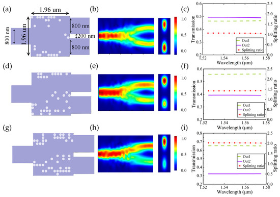
Figure 4.
(a,d,g) Top views of the 1 × 2 power splitter for different splitting ratios of 1:1, 1:1.5, and 1:2; (b,e,h) optical field distributions and the cross-sectional energy intensity profiles of the output channels for different splitting ratios of 1:1, 1:1.5, and 1:2; (c,f,i) transmittance distributions and the splitting ratios for different splitting ratios of 1:1, 1:1.5, and 1:2. Out1, Out2 represent the upper and lower output channels, respectively.
During optical signal propagation, energy loss is inevitable, resulting in incomplete transmission of the input optical power to the output ports. Therefore, the device performance is evaluated based on insertion loss, defined by the following function:
where Tout1 and Tout2 represent the average transmittance of the upper and lower output ports, respectively, and Tin denotes the average transmittance of the input waveguide. Figure 5 presents the insertion loss characteristics of the 1 × 2 OPS for various splitting ratios, where the 1:1, 1:1.5, and 1:2 ratios are represented by the red, green, and violet curves, respectively. The insertion loss of the device remains below 0.22 dB across the designed wavelength range of 1525 nm to 1575 nm, demonstrating that the designed OPS achieves excellent transmission efficiency. Specifically, the structure with a splitting ratio of 1:1.5 exhibits the highest average insertion loss of 0.22 dB, while the structures with ratios of 1:1 and 1:2 show lower insertion losses of 0.19 dB and 0.11 dB, respectively.
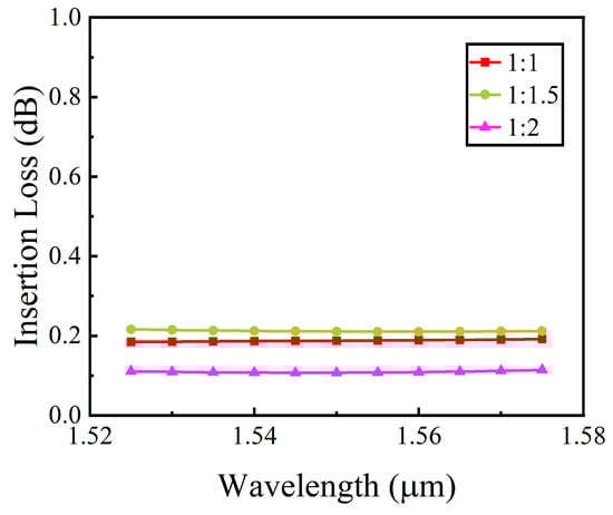
Figure 5.
Insertion losses of 1 × 2 power splitter for different splitting ratios (1:1,1:1.5, and 1:2).
3. 1 × 3 and 1 × 4 Power Splitters
The designed 1 × 2 OPS with an adjustable splitting ratio exhibits excellent device performance. This design method can be extended to develop OPSs with arbitrary splitting ratios. In this case, the OPS output channel count is extended to three and four. The three-channel and four-channel power splitters with arbitrary splitting ratios are designed and optimized using 3D FDTD simulations in conjunction with the DBS algorithm. The top view of the three-channel OPS with an adjustable splitting ratio is illustrated in Figure 6. The footprint of the 1 × 3 MMI design region is 2.8 × 2.8 µm2. The spacing between the output waveguides is 200 nm. According to the manufacturing process, the MMI region is discretized into 400 (20 × 20) small square pixels. For the three-channel OPS, splitting ratios of 1:2:1 and 2:1:2 are selected for optimization, following the same design process as the two-channel OPS. The FOM is defined as follows:
where Pout1, Pout2, and Pout3 represent the average optical powers at the upper, middle, and lower output ports of the device, respectively. Here, a, b, and c denote the target average transmittance of the upper, middle, and lower output ports for a specific PSR. Based on the selected splitting ratios (1:2:1 and 2:1:2), the corresponding values of a, b, and c were set to 0.25:0.5:0.25 and 0.4:0.2:0.4, respectively.
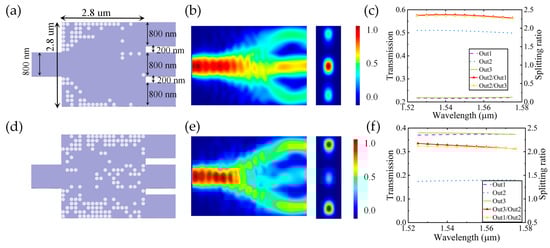
Figure 6.
(a,d) Top views of the 1 × 3 power splitter for different splitting ratios of 1:2:1 and 2:1:2; (b,e) optical field distributions and the cross-sectional energy intensity profiles of the output channels for different splitting ratios of 1:2:1 and 2:1:2; (c,f) transmittance distributions and the splitting ratios for different splitting ratios of 1:2:1 and 2:1:2. Out1, Out2, and Out3 represent the upper, middle, and lower output channels, respectively.
Figure 6b,e display the optical field distributions and corresponding cross-sectional intensity profiles for devices with various PSRs. The optical field intensity distributions confirm that the designed devices successfully achieve the target PSRs. Figure 6c,f present the performance analysis of the three-channel OPS based on 3D FDTD simulations, showing both the output port transmittance distributions and splitting ratio characteristics. Within the designed wavelength range of 1525 nm to 1575 nm, the transmittance of the three-channel OPS exceeds 90%. For the power splitters with target ratios of 1:2:1 and 2:1:2, the measured average transmission efficiencies reach 94.24% and 92.84%, respectively.
Figure 7a displays the insertion loss characteristics of the three-channel power splitter for different splitting ratios, with the 1:2:1 and 2:1:2 ratio cases represented by red and green curves, respectively. Across the design wavelength range (1525–1575 nm), the device maintains an insertion loss under 0.34 dB. Specifically, the 2:1:2 configuration demonstrates a marginally higher insertion loss of 0.34 dB, while the 1:2:1 structure achieves 0.28 dB across the operational bandwidth.
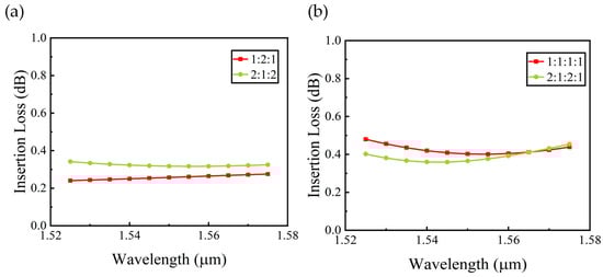
Figure 7.
(a) Insertion losses of 1 × 3 power splitter for different splitting ratios (1:2:1 and 2:1:2); (b) insertion losses of 1 × 4 power splitter for different splitting ratios (1:1:1:1 and 2:1:2:1).
Similarly, the top view of the four-channel OPS with an adjustable splitting ratio is shown in Figure 8. The 1 × 4 MMI design region has dimensions of 2.8 × 4.2 µm2 and is discretized into 600 (20 × 30) square pixel elements. The spacing between the output waveguides is 300 nm. For the four-channel OPS, splitting ratios of 1:1:1:1 and 2:1:2:1 are selected for optimization. The FOM is defined as follows:
where Pout1, Pout2, Pout3, and Pout4 represent the average optical powers at the upper, middleup, middledown, and lower output ports of the device, respectively. Here, a, b, c, and d denote the target average transmittance of the upper, middleup, middledown, and lower output ports for a specific PSR. Based on the selected splitting ratios (1:1:1:1 and 2:1:2:1), the corresponding values of a, b, c, and d were set to 0.25:0.25:0.25:0.25 and 0.332:0.166:0.332:0.166, respectively.
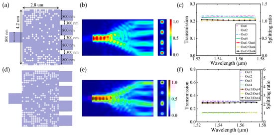
Figure 8.
(a,d) Top view of the 1 × 4 power splitter for different splitting ratios of 1:1:1:1 and 2:1:2:1; (b,e) optical field distributions and the cross-sectional energy intensity profiles of the output channels for different splitting ratios of 1:1:1:1 and 2:1:2:1; (c,f) transmittance distributions and the splitting ratios for different splitting ratios of 1:1:1:1 and 2:1:2:1. Out1, Out2, Out3, and Out4 represent the upper, middleup, middledown, and lower output channels, respectively.
Figure 8b,e present the optical field distributions and corresponding cross-sectional intensity profiles of the four-channel OPS for different PSRs. Figure 8c,f present the transmittance distributions and power splitting ratio characteristics of the output ports. Across the designed wavelength range (1525–1575 nm), the four-channel power splitter maintains transmittance above 90%. Specifically, devices with target ratios of 1:1:1:1 and 2:1:2:1 achieve average transmission efficiencies of 90.73% and 91.46%, respectively. Figure 7b presents the insertion loss performance for various splitting ratios, where the 1:1:1:1 and 2:1:2:1 configurations are indicated by red and green curves, respectively. Throughout the operational wavelength range from 1525 nm to 1575 nm, the device exhibits consistent insertion losses below 0.48 dB. Specifically, the 1:1:1:1 configuration demonstrates a marginally higher insertion loss of 0.48 dB, while the 2:1:2:1 structure achieves 0.45 dB across the operational bandwidth.
4. Fabrication Tolerance Analysis
The MMI coupling region in inverse-designed devices typically exhibits substantial structural randomness, potentially leading to hysteresis effects during fabrication and elevated optical losses. In contrast, the devices designed in this study incorporate uniformly dimensioned etching holes, significantly reducing hysteresis-induced performance degradation. However, slight over-etching or under-etching is inevitable during nanophotonic device fabrication. Therefore, a comprehensive tolerance analysis of critical fabrication parameters is essential. Taking the 1 × 2 power splitter with tunable splitting ratios as a representative example, we systematically analyzed the influence of etch hole diameter and depth variations on device performance.
Initially, we systematically evaluated the influence of etch hole diameter variations on device performance, with specific emphasis on insertion loss characteristics. Figure 9 clearly shows the insertion losses of different splitting ratios of 1:1, 1:1.5, and 1:2. The analysis was conducted with 5 nm incremental variations in etch hole diameter across a ±10 nm range. As clearly shown in Figure 9a–c, the insertion loss of the device increases with increasing etch hole diameters. When the etch hole diameter increases by 10 nm, the average insertion loss for devices with splitting ratios of 1:1, 1:1.5, and 1:2 increases to 0.2 dB, 0.24 dB, and 0.12 dB, respectively. The simulation results confirm that ±10 nm variations in etch hole diameter maintain device performance within acceptable limits across the operational wavelength range of 1525 nm to 1575 nm. Additionally, the output PSR of the power splitter is a critical parameter for evaluating device performance. Consequently, the influence on the output PSR is incorporated into the fabrication tolerance analysis. To evaluate the device fabrication tolerance, we defined an error function to characterize the PSR between the output ports. Specifically, the error function is defined as follows:
where e represents the target PSR between the upper and lower output ports and Pout1 and Pout2 denote the average optical power of the upper and lower output ports, respectively. The calculated error curves for various splitting ratios are shown in Figure 9d. The calculated maximum splitting ratio errors are 6.76%, 11.62%, and 14.44% for the 1:1, 1:1.5, and 1:2 splitting ratios, respectively.
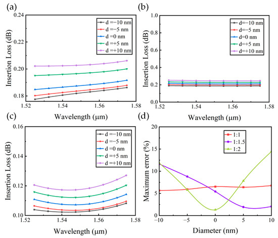
Figure 9.
(a–c) Insertion losses of various etch diameters for different ratios of 1:1, 1:1.5, and 1:2; (d) maximum errors of various etch diameters for different ratios of 1:1, 1:1.5, and 1:2.
We subsequently investigated the influence of etch hole depth variations on device performance. Figure 10 presents the corresponding insertion loss and maximum splitting ratio error characteristics as variations in etch depth. The analysis was performed with 5 nm increments across a ±10 nm etch depth variation range. As evidenced by the data, the device maintains insertion losses below 0.22 dB and splitting ratio errors under 6.51% throughout this parameter range. The results demonstrate that the performance of the designed OPSs with adjustable splitting ratios exhibits small fluctuations within the evaluated fabrication tolerance range, allowing for processing variations of up to ±10 nm in etch hole diameter and ±10 nm in etch hole depth.
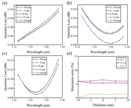
Figure 10.
(a–c) Insertion losses of various etch thicknesses for different ratios of 1:1, 1:1.5, and 1:2; (d) maximum errors of various etch thicknesses for different ratios of 1:1, 1:1.5, and 1:2.
5. Discussion
After a series of simulations and data analyses, the proposed 1 × 2 power splitter with an adjustable PSR based on the Si3N4 platform demonstrates excellent performance, including low insertion loss (<0.22 dB) and high transmittance (>90%). Moreover, the device achieves an ultra-compact footprint of only 1.96 × 1.96 μm2. Theoretically, the design method in this paper enables the realization of power splitters with arbitrary splitting ratios, offering high design flexibility. To demonstrate the feasibility and versatility of this approach, three representative ratios are selected as examples. Considering possible deviations in etch hole depth and diameter during fabrication, a tolerance analysis was conducted separately for these two critical parameters. The results indicate that the device maintains stable performance under dimensional variations of up to ±10 nm, indicating strong robustness to fabrication imperfections. Furthermore, the design methodology is scalable and can be applied to the development of multi-channel power splitters with adjustable PSRs. Due to the increased device footprint and longer optimization time associated with multi-channel devices, this work focuses on the design of three-channel and four-channel power splitters with adjustable PSRs. Simulation results confirm that the designed devices maintain excellent performance.
It is important to note that, in contrast to conventional symmetric power splitters, the device with 1:1 PSR exhibits an asymmetric structure. This asymmetry results from a design strategy that simultaneously optimizes both the splitting ratio and the overall transmission efficiency. During the automated optimization process, the algorithm identifies structural devices that simultaneously ensure high transmission efficiency and low deviation from the target splitting ratio. Table 1 presents a comprehensive performance comparison between the proposed OPSs and previously reported designs. It demonstrates that the proposed power splitter design achieves both port-count scalability and excellent performance, including compact size and reduced insertion loss. Therefore, the proposed device exhibits promising potential for practical applications in signal detection and feedback, power equalization circuits, and nanophotonic phased arrays.

Table 1.
Comparison of demonstrated OPSs with an adjustable PSR.
6. Conclusions
In conclusion, we have demonstrated integrated OPSs with arbitrary splitting ratios using an inverse design approach, where the DBS algorithm was employed for device optimization. A 1 × 2 power splitter with splitting ratios of 1:1, 1:1.5, and 1:2 was successfully implemented across the 1525–1575 nm operational bandwidth. To demonstrate the scalability of the designed devices based on this design methodology, we further implemented a 1 × 3 power splitter with 1:2:1 and 2:1:2 splitting ratios and a 1 × 4 power splitter with 1:1:1:1 and 2:1:2:1 splitting ratios. The designed power splitters exhibit ultra-compact footprints of 1.96 × 1.96 μm2, 2.8 × 2.8 μm2, and 2.8 × 4.2 μm2, respectively. The achieved performance shows minimal discrepancy from the design objectives. The adopted design approach demonstrates effectiveness in realizing high-performance devices through automated design.
Author Contributions
Conceptualization, H.L. and Y.C.; methodology, S.L. and Y.C.; software, Y.C.; validation, Y.C., S.L., F.L. and H.W.; formal analysis, S.L. and Y.C.; investigation, Y.C.; resources, H.L.; data curation, Y.C.; writing—original draft preparation, Y.C.; writing—review and editing, H.L. and Y.C.; visualization, Y.C.; supervision, X.L., F.L., S.L. and Y.L.; project administration, Y.C., Y.L., S.L. and Q.G.; funding acquisition, H.L. All authors have read and agreed to the published version of the manuscript.
Funding
This research was funded by the Foundation of Liaoning Province Education Administration (JYTMS20230429).
Institutional Review Board Statement
Not applicable.
Informed Consent Statement
Not applicable.
Data Availability Statement
The raw data supporting the conclusions of this article will be made available by the authors on request.
Conflicts of Interest
The authors declare no conflicts of interest.
References
- Hansi, M.; Te, D.; Xinpeng, J.; Junbo, Y. Inverse-designed silicon-based on-chip power splitters. Opto-Electron. Eng. 2023, 50, 230086-1–230086-18. [Google Scholar]
- Kasai, K.; Nakazawa, M.; Ishikawa, M.; Ishii, H. 8 kHz linewidth, 50 mW output, full C-band wavelength tunable DFB LD array with self-optical feedback. Opt. Express 2018, 26, 5675–5685. [Google Scholar] [CrossRef] [PubMed]
- Velha, P.; Sorianello, V.; Preite, M.V.; De Angelis, G.; Cassese, T.; Bianchi, A.; Testa, F.; Romagnoli, M. Wide-band polarization controller for Si photonic integrated circuits. Opt. Lett. 2016, 41, 5656–5659. [Google Scholar] [CrossRef] [PubMed]
- Qiu, J.; Tian, Y.; Huang, Z.; Wang, Y.; Kong, D.; Wu, J. Integrated In-band OSNR monitor based on asymmetrical parallel-MZIs for WDM signals. IEEE J. Sel. Top. Quantum Electron. 2016, 22, 467–472. [Google Scholar] [CrossRef]
- Xie, F.; Zhu, S.; Zhang, Z. Design of an optical power splitter with adjustable split ratio. Chin. Opt. 2023, 16, 1121–1128. [Google Scholar] [CrossRef]
- Li, Z.; Huang, X.; Liu, Y.; Kuang, Y.; Guan, H.; Tian, L.; Li, Z.; Han, W. Ultra-compact low-loss variable-ratio 1 × 2 power splitter with ultra-low phase deviation based on asymmetric ladder-shaped multimode interference coupler. Opt. Express 2020, 28, 34137–34146. [Google Scholar] [CrossRef] [PubMed]
- Zhang, L.; Fu, X.; Yang, L. Polarization-independent, lithium-niobate-on-insulator directional coupler based on a combined coupling-sections design. Appl. Opt. 2020, 59, 8668–8673. [Google Scholar] [CrossRef] [PubMed]
- Lin, Z.; Shi, W. Broadband, low-loss silicon photonic Y-junction with an arbitrary power splitting ratio. Opt. Express 2019, 27, 14338–14343. [Google Scholar] [CrossRef] [PubMed]
- Mao, D.; Wang, Y.; El-Fiky, E.; Xu, L.; Kumar, A.; Jaques, M.; Samani, A.; Carpentier, O.; Bernal, S.; Alam, M.S. Adiabatic coupler with design-intended splitting ratio. J. Light. Technol. 2019, 37, 6147–6155. [Google Scholar] [CrossRef]
- Zhu, J.; Chao, Q.; Huang, H.; Zhao, Y.; Li, Y.; Tao, L.; She, X.; Liao, H.; Huang, R.; Zhu, Z. Compact, broadband, and low-loss silicon photonic arbitrary ratio power splitter using adiabatic taper. Appl. Opt. 2021, 60, 413–416. [Google Scholar] [CrossRef] [PubMed]
- Sia, J.X.B.; Wang, W.; Guo, X.; Zhou, J.; Zhang, Z.; Rouifed, M.S.; Li, X.; Qiao, Z.L.; Liu, C.Y.; Littlejohns, C. Mid-infrared, ultra-broadband, low-loss, compact arbitrary power splitter based on adiabatic mode evolution. IEEE Photonics J. 2019, 11, 6601111. [Google Scholar] [CrossRef]
- Lin, Y.; Ke, W.; Ma, R.; Huang, F.; Tan, H.; Xu, J.; Lin, Z.; Cai, X. Arbitrary-ratio 1 × 2 optical power splitter based on thin-film lithium niobate. Opt. Express 2023, 31, 27266–27273. [Google Scholar] [CrossRef] [PubMed]
- Liao, S.; Bao, H.; Zhang, T.; Liu, J.; Liao, X.; Liu, L. Integrated optical power splitter with continuously adjustable power splitting ratio. IEEE Photonics J. 2020, 12, 7801513. [Google Scholar] [CrossRef]
- Yu, Z.; Cui, H.; Sun, X. Genetically optimized on-chip wideband ultracompact reflectors and Fabry–Perot cavities. Photonics Res. 2017, 5, B15–B19. [Google Scholar] [CrossRef]
- Wang, K.; Ren, X.; Chang, W.; Lu, L.; Liu, D.; Zhang, M. Inverse design of digital nanophotonic devices using the adjoint method. Photonics Res. 2020, 8, 528–533. [Google Scholar] [CrossRef]
- Lu, L.; Liu, D.; Zhou, F.; Li, D.; Cheng, M.; Deng, L.; Fu, S.; Xia, J.; Zhang, M. Inverse-designed single-step-etched colorless 3 dB couplers based on RIE-lag-insensitive PhC-like subwavelength structures. Opt. Lett. 2016, 41, 5051–5054. [Google Scholar] [CrossRef] [PubMed]
- Shen, B.; Wang, P.; Polson, R.; Menon, R. An integrated-nanophotonics polarization beamsplitter with 2.4 × 2.4 μm2 footprint. Nat. Photonics 2015, 9, 378–382. [Google Scholar] [CrossRef]
- Ma, H.; Huang, J.; Zhang, K.; Yang, J. Arbitrary-direction, multichannel and ultra-compact power splitters by inverse design method. Opt. Commun. 2020, 462, 125329. [Google Scholar] [CrossRef]
- Zhang, Y.; Zhang, Y.; Yin, M.; Wei, X.; Ma, H.; Zhao, F.; Zhang, Z.; He, X.; Chen, H.; Yu, Y. Vertical direction high-bandwidth multilayer tunable power splitter based on PSO and DBS algorithms. Opt. Eng. 2024, 63, 087102. [Google Scholar]
- Wu, Z.; Wen, J.; Zhang, H.; Wang, Q.; Yu, H.; Pan, Y.; Zhang, Y.; Liu, Z. Inverse design of an ultra-compact and large-bandwidth bent subwavelength grating wavelength demultiplexer. Appl. Opt. 2023, 62, 8292–8298. [Google Scholar] [CrossRef] [PubMed]
- Ma, W.; Cheng, F.; Liu, Y. Deep-learning-enabled on-demand design of chiral metamaterials. ACS Nano 2018, 12, 6326–6334. [Google Scholar] [CrossRef] [PubMed]
- Tahersima, M.H.; Kojima, K.; Koike-Akino, T.; Jha, D.; Wang, B.; Lin, C.; Parsons, K. Deep neural network inverse design of integrated photonic power splitters. Sci. Rep. 2019, 9, 1368. [Google Scholar] [CrossRef] [PubMed]
- Xu, K.; Liu, L.; Wen, X.; Sun, W.; Zhang, N.; Yi, N.; Sun, S.; Xiao, S.; Song, Q. Integrated photonic power divider with arbitrary power ratios. Opt. Lett. 2017, 42, 855–858. [Google Scholar] [CrossRef] [PubMed]
- Liu, Y.; Li, Z.; Wang, S.; Zhang, N.; Yao, Y.; Du, J.; He, Z.; Song, Q.; Xu, K. Ultra-compact and polarization-insensitive MMI coupler based on inverse design. In Proceedings of the 2019 Optical Fiber Communications Conference and Exhibition (OFC), San Diego, CA, USA, 3–7 March 2019; pp. 1–3. [Google Scholar]
- Xie, H.; Liu, Y.; Sun, W.; Wang, Y.; Xu, K.; Du, J.; He, Z.; Song, Q. Inversely designed 1 × 4 power splitter with arbitrary ratios at 2-μm spectral band. IEEE Photonics J. 2018, 10, 2700506. [Google Scholar] [CrossRef]
- Meng, C.; Qiu, J.; Tian, Y.; Ye, Z.; Wu, J. A broadband compact 1 × 3 power splitter designed with inverse design method. In Proceedings of the 2016 15th International Conference on Optical Communications and Networks (ICOCN), Hangzhou, China, 24–27 September 2016; pp. 1–3. [Google Scholar]
- Patsamanis, G.; Ketzaki, D.; Chatzitheocharis, D.; Chrysostomidis, T.; Roumpos, I.; Sacchetto, D.; Zervas, M.; Vyrsokinos, K. Silicon nitride asymmetric 1 × 2 power splitter based on multimode interference. In Proceedings of the Integrated Optics: Devices, Materials, and Technologies XXV, Online, 6–12 March 2021; pp. 236–241. [Google Scholar]
Disclaimer/Publisher’s Note: The statements, opinions and data contained in all publications are solely those of the individual author(s) and contributor(s) and not of MDPI and/or the editor(s). MDPI and/or the editor(s) disclaim responsibility for any injury to people or property resulting from any ideas, methods, instructions or products referred to in the content. |
© 2025 by the authors. Licensee MDPI, Basel, Switzerland. This article is an open access article distributed under the terms and conditions of the Creative Commons Attribution (CC BY) license (https://creativecommons.org/licenses/by/4.0/).