Article

Creation of Low-Loss Dual-Ring Optical Filter via Temporal Coupled Mode Theory and Direct Binary Search Inverse Design

College of Future Information Technology, Fudan University, Shanghai 200438, China
*
Authors to whom correspondence should be addressed.
Photonics 2025, 12(7), 681; https://doi.org/10.3390/photonics12070681
Submission received: 9 June 2025 / Revised: 3 July 2025 / Accepted: 4 July 2025 / Published: 6 July 2025

Abstract

We propose a dual-ring optical filter based on direct binary search inverse design. The proposed device comprises two cascaded rings in an add–drop configuration. A physical model was established using temporal coupled mode theory to derive theoretical spectra and analyze key parameters governing transmission performance. Based on theoretical results, a direct binary search algorithm was implemented. The parameters of the proposed device were calculated using a three-dimensional finite-difference time-domain method for verification. The numerical results demonstrate a free spectral range of 86 nm, with insertion loss and extinction ratios of 0.3 dB and 22 dB, respectively. The proposed device has a narrow spectral linewidth of 0.3 nm within a compact footprint of 24   μ m × 25.5   μ m . The device shows significant application potential in laser external cavities and dense wavelength division multiplexing systems. Moreover, this work provides a novel methodology for precision design of photonic devices.

1. Introduction

Silicon photonic devices have emerged as core components in modern optical communications, sensing, and quantum optical systems owing to their low loss, high integration density, and immunity to electromagnetic interference [1,2,3,4,5]. As pivotal elements in photonic integrated circuits (PICs), optical filters play critical roles in wavelength selection, channel isolation, and signal modulation [6,7,8]. Conventional single-ring optical filters are widely deployed in optical communication systems owing to their high-quality factors and compact footprints. Their free spectral range (FSR = λ2/(ng·L)) is inversely proportional to the resonator circumference L and results in typical FSR values of merely a few nanometers in the 1550 nm band, which is insufficient for dense wavelength division multiplexing (DWDM) broad-tuning requirements [9,10]. Recently, cascaded rings in add–drop configurations have significantly extended the FSR via the Vernier effect, theoretically expanding the tuning range by orders of magnitude compared to single-ring designs, thereby emerging as an effective solution for high-performance filters [11]. In 2022, Guo et al. [12] proposed a dual-ring filter based on the Vernier effect. The designed filter is made of two cascaded add–drop racetrack MRRs with slightly different perimeters of 725   μ m and 740   μ m . By using finite-difference time-domain (FDTD) for parameter calculation, the numerical results show that the FSR can reach 95 nm near the 1550 nm wavelength. However, the total length of the device is about 8 mm, and the insertion loss varies by 1.5 dB in the 1480–1660 nm wavelength. In 2023, Calo et al. [13] proposed a hybrid InP-SiN dual-ring filter, which is based on SiN waveguides with low propagation losses (0.1 dB/cm), and its moderate refractive index contrast enables a tighter bending radius. The structure of the proposed device is relatively compact and the power coupling coefficient of the micro-ring resonator (MRR) is thoroughly dimensioned. The FSR is only 45 nm. In 2024, Lin et al. [14] demonstrated an ultra-broadband Vernier-cascaded dual-ring filter. The proposed device comprises two cascaded add–drop MRRs with slightly different radii. Finite-different eigenmode simulations were used in Lumerical for parameter calculation, and the Si3N4 MRR dispersion characteristics were simulated. The numerical results show that the insertion loss, extinction ratio, and FSR of the designed device are 1 dB, 5.78 dB, and 72 nm, respectively. Although an extinction ratio of more than 5 dB is sufficient for lasing, when it comes to DWDM systems, such extinction ratio will cause significant channel crosstalk. Moreover, further optimization of the insertion loss of this device is still necessary. The design methodologies mentioned above have remained empirically driven in recent years [15,16,17], where researchers identify structural features meeting specific performance metrics such as transmittance, the FSR, and the extinction ratio based on manual design. Such approaches consider limited structural parameters while neglecting coupling losses from rings and waveguides, which often converge to local optima and fail in high-precision and densely integrated devices. Recent advances in global optimization techniques, such as genetic algorithms (GAs) and particle swarm optimization (PSO), address local optimum issues in silicon photonic device design. However, their population-based iteration mechanisms exhibit exponentially deteriorating convergence rates when optimizing more than five parameters [18]. In contrast, as a gradient-free optimization algorithm, direct binary search (DBS) provides a potential solution to these challenges. Its core methodology discretizes the parameter space through binary encoding and employs sequential single-parameter perturbation to evaluate performance improvements, enabling local minimum avoidance and compatibility with both discrete and continuous variables [19]. In recent years, DBS has been successfully implemented in the design of certain silicon photonic devices. In 2023, Lin et al. [20] proposed a low-loss and broadband polarization-insensitive high-order mode pass filter based on the DBS algorithm. The 3D-FDTD method is used to simulate the performance of the device. The DBS algorithm is used to optimize the coupling structure between multi-mode waveguides. The numerical results show that an insertion loss smaller than 0.86 dB and an extinction ratio larger than 16.8 dB are obtained for the filter working at TE polarization within a bandwidth ranging from 1520 to 1590 nm, while in the case of TM polarization, an insertion loss lower than 0.79 dB and an extinction ratio greater than 17.5 dB are obtained. In 2024, Wang et al. [21] proposed a 1 × 2 ultra-compact 2.4 × 3.6   μ m 2 multimode wavelength demultiplexer based on the DBS algorithm, which can simultaneously perform wavelength demultiplexing and mode conversion. The pre-designed FOM guides the algorithm in optimizing the transmittance of the device. The simulation results show that the lowest insertion loss and extinction ratio are 0.759 dB and 10.06 dB, respectively. In the same year, Zhou et al. [22] designed a 1 × 2 photonic switch based on the silicon-on-insulator platform, assisted by the DBS algorithm, and based on the parameter sweeping results. The device exhibits a tiny footprint of only 3 × 4   μ m 2 with an insertion loss lower than 0.5 dB and an extinction ratio over 20 dB. Recent reports [23,24] indicate that designed photonic devices assisted by the DBS algorithm exhibit a common advantage, that is, exceptional optimization of their coupling structures. Through continuous nanostructure iteration, lower losses are achievable while maintaining compact footprints. However, little research has been conducted to date regarding the application of DBS in dual-ring optical filter design. The coupling between the ring and the waveguide is the core of the dual-ring filter device. For feasible implementation of DBS in a dual-ring optical filter, a systematic analysis of the MRRs’ coupling structures is crucial. Commonly, the transmission characteristics of this coupling structure can be analyzed by using the time-domain coupled mode theory (TCMT). Hence, there is considerable interest in combining TCMT with the DBS algorithm to create dual-ring optical filters with excellent performance and compact structures.
We propose a low-loss dual-ring optical filter based on TCMT and the DBS algorithm. First, we established a physical model of cascaded dual-ring systems using TCMT. Second, the desired transmission performance was encoded into a DBS figure of merit (FOM) to optimize coupling coefficients between ring resonators and waveguides. Finally, theoretical parameters were used to perform 3D-FDTD simulations to verify the theoretical results for the proposed dual-ring optical filter. The numerical results demonstrate a 0.3 dB insertion loss, an 86 nm FSR, a 0.3 nm linewidth, and a 22 dB extinction ratio for the designed filter. The proposed device has significant application potential in laser external cavities and DWDM systems. This study also provides novel theoretical tools and technical pathways for high-precision multi-ring optical filter design.

2. Theoretical Analysis

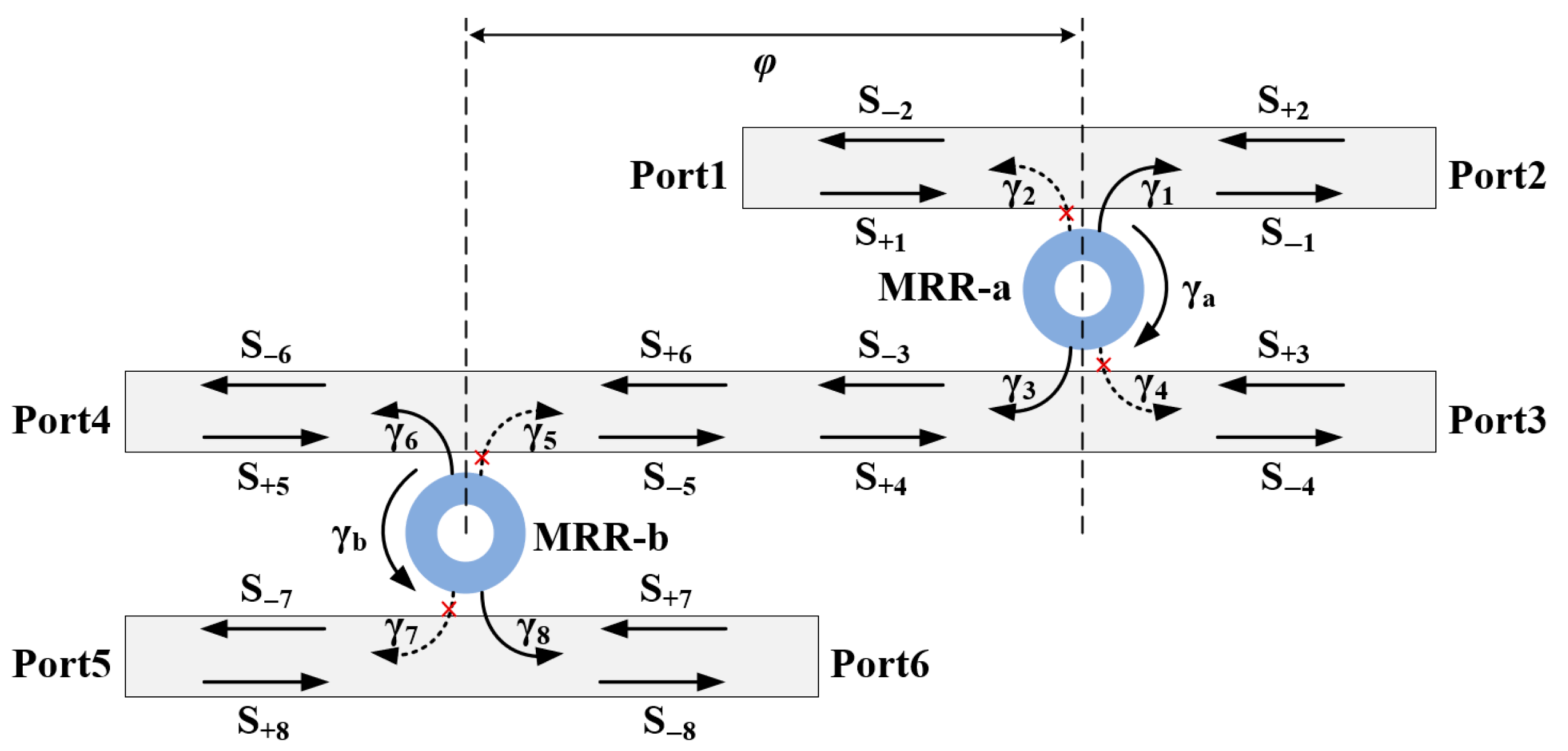
2.1. Theoretical Analysis of Dual-Ring Optical Filter

The filter structure proposed in this study comprises two MRRs and three waveguides in cascade. The theoretical model of the dual-ring optical filter is shown in Figure 1. In the cascaded dual-ring system, the coupling process occurs as follows: when the wavelength of light incident from Port 1 coincides with the resonant wavelengths of both MRR-a and MRR-b, the optical wave sequentially couples into both MRRs. Eventually, most of the light intensity is output from Port 6, while all other ports exhibit negligible energy output. We analyze the transmission characteristics of the model in Figure 1 based on TCMT. In Figure 1, S + i and S i represent the amplitude of the input and output waves, respectively (i = 1, 2, 3, 4, 5, 6). The coupling attenuation coefficient γ i (i = 1, 2, 3… 8) determines the coupling efficiency between the ring and the waveguide. ϕ represents the phase delay of the light wave transmitted from MRR-a to MRR-b. Parameters γ a and γ b denote the intrinsic amplitude attenuation coefficients of MRR-a and MRR-b, respectively. The intrinsic quality factor Q int and intrinsic loss rate α satisfy the relationship Q int = 2 π n e f f L λ v g α . The smaller the γ a or γ b value (reduced α ), the higher the intrinsic quality factor Q int . Due to the radius mismatch between the two rings, we define the resonant frequencies as ω 1 and ω 2 and the resonant mode amplitudes as a and b for MRR-a and MRR-b, respectively. Let the incident light frequency be ω . The temporal coupled mode equations for this structure are then given.
For MRR-a, the time domain variation in the resonant mode amplitude can be expressed as
d a d t = i ω 1 a ( γ 1 + γ 3 + γ a ) a + 2 γ 1 S + 1 + 2 γ 3 S + 3
According to power conservation and time-reversal symmetry, the relationship between input and output waves is given as follows:
S 1 = S + 1 2 γ 1 a
S 3 = S + 3 2 γ 3 a
Since the frequency ω of the incident light is constant, i.e., a ( t ) = e i ω t , then da/dt = −iωa. By substituting it into Equation (1), we can get
i ( ω ω 1 ) a + ( γ 1 + γ 3 + γ a ) a = 2 γ 1 S + 1 + 2 γ 3 S + 3
For MRR-b, the time domain variation in the resonant mode amplitude is given by
d b d t = i ω 2 b ( γ 6 + γ 8 + γ b ) b + 2 γ 6 S + 6 + 2 γ 8 S + 8
Similarly, the relationship between the input and output waves is given as follows:
S + 6 = S 3 e j ϕ
S 8 = S + 8 2 γ 8 b
Since the frequency ω of the incident light is constant, i.e., b ( t ) = e i ω t , then db/dt = −iωb. By substituting it into Equation (5) and combining Equation (6), we can get
i ( ω ω 2 ) b + ( γ 6 + γ 8 + γ b ) b = S 3 e j ϕ + 2 γ 8 S + 8
It is assumed that S + 2 = S + 3 = S + 5 = S + 7 = S + 8 = 0 , which means that there is no light input at Ports 2, 3, 4, 5, and 6. Since the light waves are only input from Port 1, Equations (4) and (8) can be simplified as follows:
i ( ω ω 1 ) a + ( γ 1 + γ 3 + γ a ) a = 2 γ 1 S + 1
i ( ω ω 2 ) b + ( γ 6 + γ 8 + γ b ) b = 2 γ 3 a e j ϕ
By comparing Equations (9) and (10), it can be observed that the resonant mode amplitude of MRR-a is related to the input wave amplitude, while the resonant mode amplitude of MMR-b is related to that of MRR-a. From the perspective of the optical path, this is because after the light wave is input from Port 1, it first comes into contact with MRR-a. And the maximum resonant amplitude of MRR-b is entirely determined by how much of the light wave is coupled out from MRR-a, that is, S 3 = 2 γ 3 a . Here, γ 3 represents the coupling attenuation coefficient between MMR-a and the waveguide. By properly designing the coupling structure, this parameter can be significantly influenced.
From Equation (9), we can determine the relationship between the amplitude of the input light and the resonant mode amplitude of MRR-a:
S + 1 = [ i ( ω ω 1 ) + ( γ 1 + γ 3 + γ a ) ] 2 γ 1 a
By combining Equations (7) and (11), the transmission spectrum T ( ω ) can be obtained:
T ( ω ) = S 8 S + 1 2 = 2 γ 1 γ 8 i ( ω ω 1 ) + ( γ 1 + γ 3 + γ a ) b a 2
From Equation (12), it can be seen that the theoretical transmission of the dual-ring filter is related to the ratio of the resonant mode amplitude of MRR-b and MRR-a. Ideally, one of the conditions for the theoretical transmittance to approach 1 is that b a = 1 . This implies that MRR-a and MRR-b must have exactly the same structure to ensure consistent resonant mode amplitude. However, such a structure is meaningless for the dual-ring filter that extends the FSR based on the Vernier effect. On the one hand, we can utilize MRR-a and MRR-b with slightly different radii to find a balance between the FSR and transmittance. On the other hand, the maximum transmittance can be achieved by adjusting the coupling attenuation coefficient between the ring and the waveguide, as discussed next.
From Equation (10), we can obtain the expression of b a . By substituting it into Equation (12), the theoretical transmittance T ( ω ) is given as follows:
T ( ω ) = S 8 S + 1 2 = 16 γ 1 γ 3 γ 6 γ 8 e j 2 ϕ ( γ 1 + γ 3 + γ a ) 2 + ( ω ω 1 ) 2 ( γ 6 + γ 8 + γ b ) 2 + ( ω ω 2 ) 2
As mentioned above, by properly designing the coupling structure, the coupling attenuation coefficient between MMR-a and the waveguide can be significantly influenced. Similarly, we can optimize the coupling structures on both sides of each ring to achieve the purpose of adjusting γ i (i = 1, 2, 3…8) to obtain the maximum transmittance.
Assuming that γ 1 = γ 3 = γ w a v a , γ 6 = γ 8 = γ w a v b , which means the structure of MRR-a and MRR-b are symmetrical. Let ω 1 = ω 2 = ω , which means the resonant frequencies of the two ring resonators and incident light are the same. By substituting the above relationship into Equation (13), the theoretical maximum transmittance T max can be expressed as follows:
T max = S 8 S + 1 2 = 4 γ w a v a 2 γ w a v a + γ a 4 γ w a v b 2 γ w a v b + γ b e j 2 ϕ
From Equation (14), it can be seen that T max can reach 1 only when ϕ = ( m + 1 / 2 ) π (where m is a non-negative integer) and γ a = γ b = 0 . The first two terms of Equation (14) can be regarded as the contributions provided by MRR-a and MRR-b to the transmittance. Taking the first term of Equation (14) as an example, Figure 2 illustrates the relationship between the numerical value and γ w a v a / γ a . As can be seen from Figure 2, when γ w a v a > > γ a , the value of the first term of Equation (14) is close to 1, which means that the theoretical model of MRR-a with intrinsic loss shown in Figure 1 can be simplified to a model without intrinsic loss for discussion. The second term of Equation (14) also follows the same pattern. However, in the actual process of structural design, it is not necessary for γ w a v a to be much larger than γ a . Usually, when γ w a v a / γ a 100 , it can be considered that the coupling model does not have intrinsic loss. Because when γ w a v a / γ a = 100 and γ w a v b / γ b = 100 , the T max value is close to 0.9803. At this time, the energy loss caused by intrinsic loss can be approximately ignored.
A larger amplitude attenuation coefficient is like a higher refractive index in a light path, while a smaller coefficient resembles a lower refractive index. Because light waves tend to follow paths with higher refractive indexes, greater differences between two paths’ indexes concentrate more energy along the high-index route. Similarly, light favors paths with larger attenuation coefficients. When the coupling attenuation coefficient exceeds the intrinsic attenuation coefficient, more energy couples into the waveguide. This implies that the coupling structures on both sides of each ring critically governs the overall transmission efficiency of the cascaded dual-ring system.

2.2. An Analysis of the Frequency Deviation

Based on the above theoretical derivation results, we further analyze the relationship between transmittance and frequency detuning. Assuming a symmetric coupling configuration between the MRR and waveguides, we set equal coupling attenuation coefficients γ 1 = γ 3 = γ 6 = γ 8 = γ w a v . According to Equation (14), the transmission spectrum T ( ω ) can be rewritten as
T ( ω ) = S 8 S + 1 2 = 16 γ w a v 4 e j 2 ϕ ( 2 γ w a v + γ a ) 2 + ( ω ω 1 ) 2 ( 2 γ w a v + γ b ) 2 + ( ω ω 2 ) 2
The MRRs are modeled as lossless resonators, that is, γ a = γ b = 0 . Let Δ = ω ω 0 represent frequency detuning with identical resonant frequencies ( ω 1 = ω 2 = ω 0 ), and Equation (15) can be simplified as
T ( ω ) = S 8 S + 1 2 = 16 γ w a v 4 e j 2 ϕ ( 2 γ w a v ) 2 + Δ 2 ( 2 γ w a v ) 2 + Δ 2
Equation (16) demonstrates that the transmission T ( ω ) achieves its maximum value of 1 when ϕ = ( m + 1 / 2 ) π (where m is a non-negative integer) and ω = ω 0 .
Figure 3 shows the relationship between the transmittance and frequency detuning of the cascaded dual-ring system. From Figure 3a, it can be seen that when the resonant frequency ω = ω 0 , the transmittance of this device can reach the highest value, and the reflectance is the lowest. As frequency detuning ω / ω 0 increases, transmittance decreases, while reflectance increases. This phenomenon satisfies the law of energy conservation. According to Figure 3b, when γ w a v takes values of 4.05 × 10 3 , 5 × 10 3 , and 6.05 × 10 3 , the transmission spectrum broadens as the coupling attenuation coefficient increases. This is because the total Q value Q t o t a l of the MRR is composed of the intrinsic Q value Q i and the coupling Q value Q c , and they satisfy the relationship Q t o t a l = 1 Q i + 1 Q c . The increase in γ w a v indicates an increase in coupling strength, making it easier for optical energy to enter the MRR from the waveguide and escape from the MRR as well. This leads to an increase in the coupling Q value Q c , which further causes the Q t o t a l value to decrease, and consequently, the linewidth broadens.

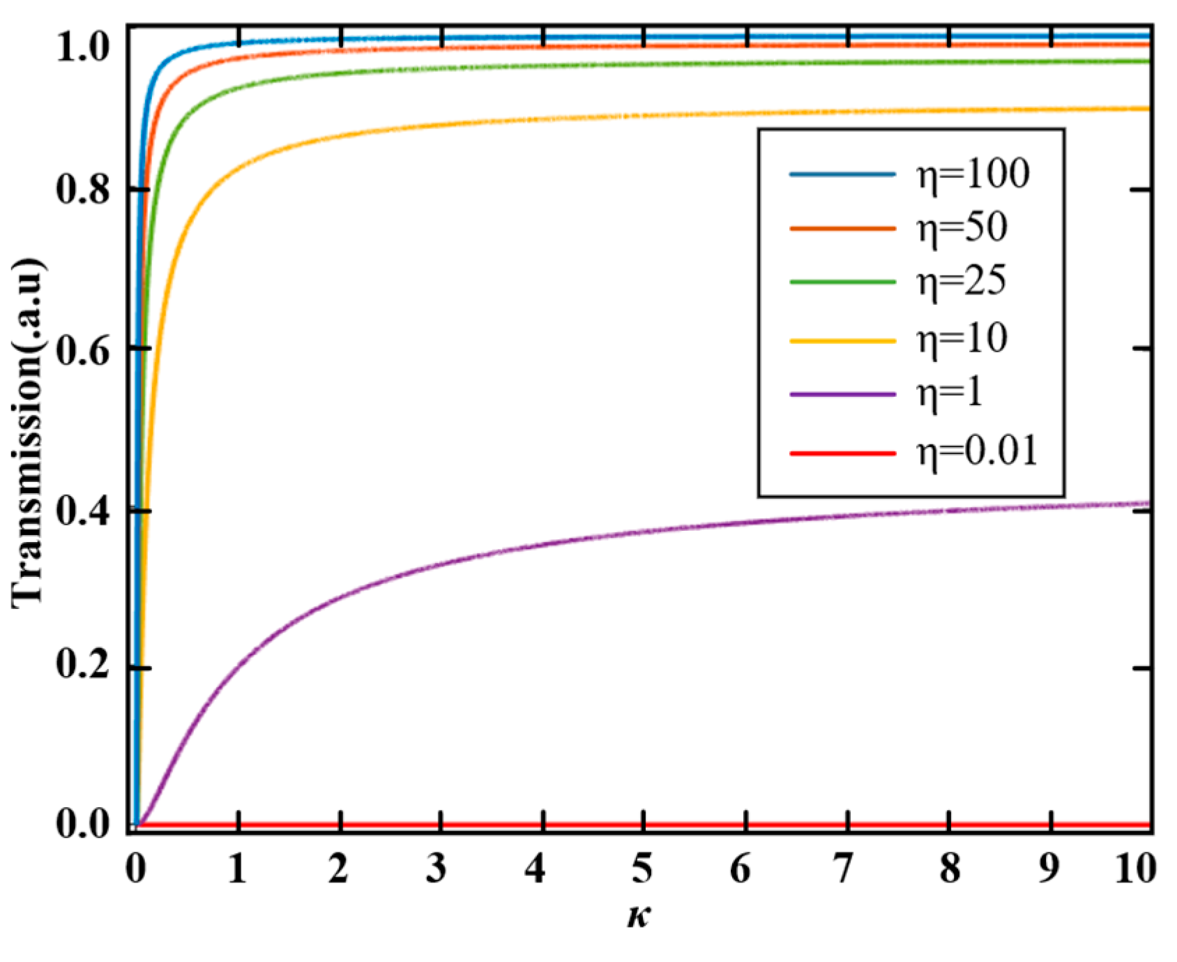
2.3. Analysis of Intrinsic Loss in MRR
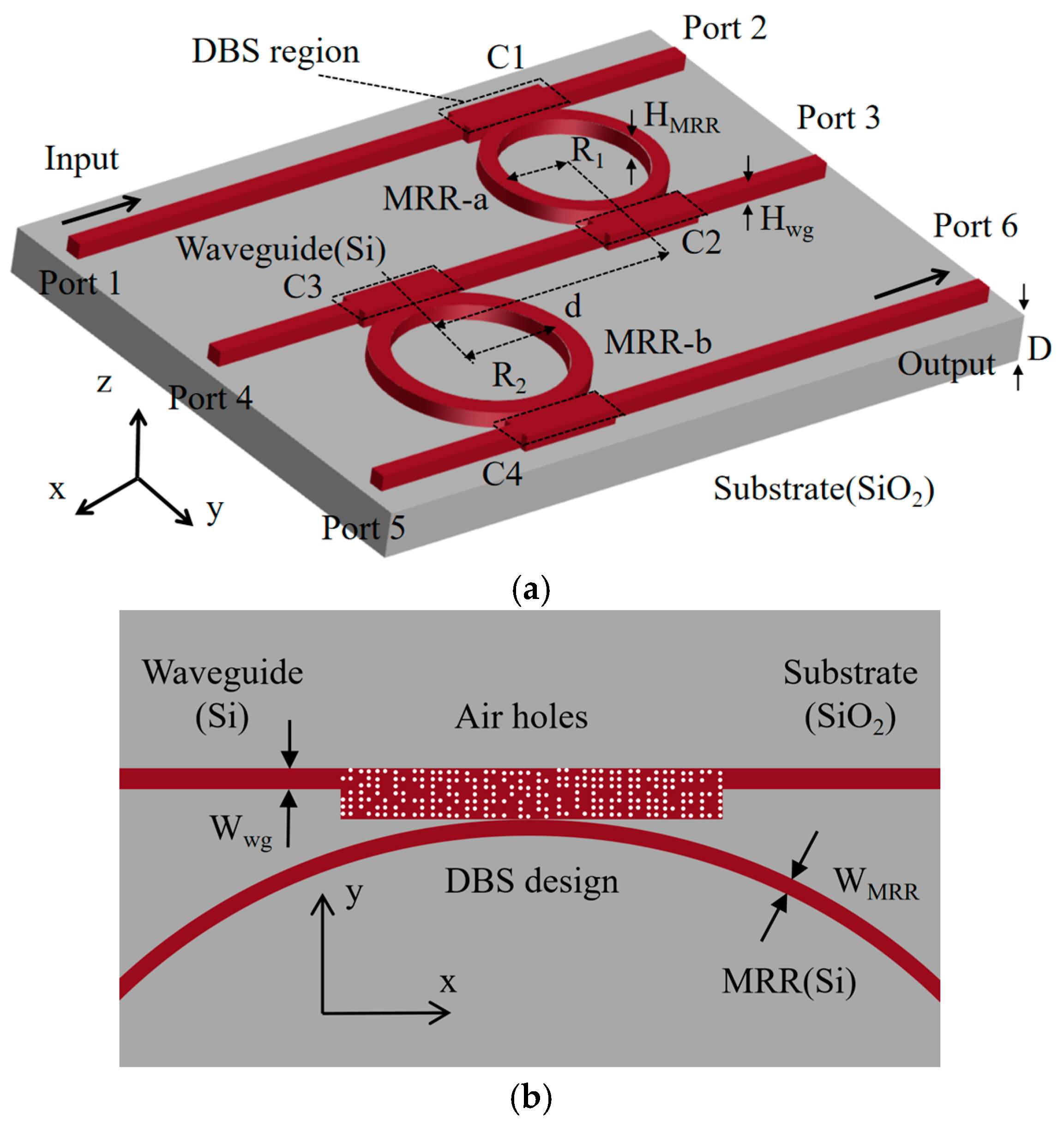
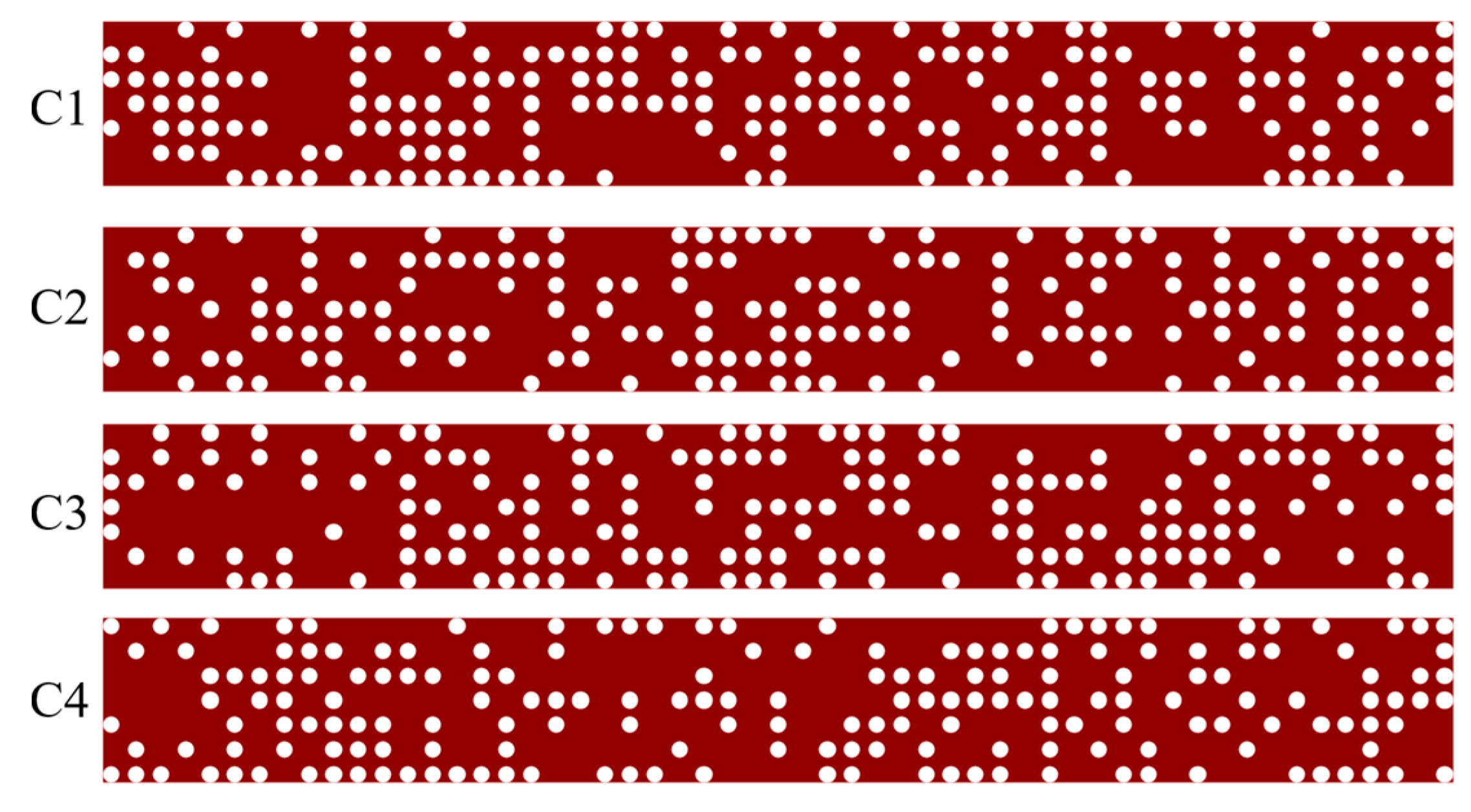
Based on the above theoretical derivation, the following discussion further explores the relationship between the transmittance of the cascaded dual-ring system and the intrinsic loss ratio when intrinsic loss exists ( γ a 0 , γ b 0 ). Assuming that the two MRRs have no frequency detuning ( ω 1 = ω 2 = ω 0 ) and the phase delay between the ring cavities satisfies ϕ = ( m + 1 / 2 ) π (where m is a non-negative integer), according to Equation (14), the transmission spectrum T ( ω 0 ) is given as follows:
T ( ω 0 ) = S 8 S + 1 2 = 16 γ w a v 4 ( 2 γ w a v + γ a ) 2 ( 2 γ w a v + γ b ) 2
Let the ratio of the intrinsic amplitude attenuation coefficients of MRR-a and MRR-b be κ = γ a / γ b and the ratio of the intrinsic amplitude attenuation coefficient and coupling attenuation coefficient of MRR-a be η = γ w a v / γ a . Substituting it into Equation (17), we obtain
T ( ω 0 ) = S 8 S + 1 2 = 16 κ 2 η 4 ( 2 η + 1 ) 2 ( 2 κ η + 1 ) 2
The variation in the attenuation coefficient ratio with transmittance, plotted according to Equation (18), is shown in Figure 4. It can be observed that the loss in the cascaded dual-ring system is closely linked to the coupling efficiency between the ring and waveguide. When η increases ( γ w a v > γ a ),transmittance rises significantly. This indicates that the intrinsic loss of MRR-a is relatively low or the coupling efficiency between MRR-a and the waveguide is enhanced. Conversely, as η decreases, transmittance drops sharply. It is worth noting that when the value of η is relatively large, transmittance remains almost unaffected by the ratio of intrinsic attenuation between the two MRRs. This is because η determines the performance of MRR-a in the cascaded system, ensuring complete energy transfer to MRR-b for output. However, when η is small, excessive attenuation in MRR-a significantly impairs energy transmission. Under such conditions, a larger κ value corresponds to a smaller γ b , leading to a slight increase in transmittance.
In conclusion, the following conditions must be satisfied in order to design a low-loss, narrow-linewidth dual-ring optical filter: (1) The phase delay between the two MRRs must satisfy ϕ = ( m + 1 / 2 ) π (where m is a non-negative integer); (2) the two MRRs must resonate without frequency detuning ( ω 1 = ω 2 = ω 0 ); and (3) the intrinsic loss of the MRRs must be minimized. According to Equation (9) and the analysis in Figure 4, the ratio γ w a v / γ a significantly affects the device’s transmittance. The theoretical results above will guide the construction of the DBS algorithm and be validated by using FDTD simulations.

3. Device Design

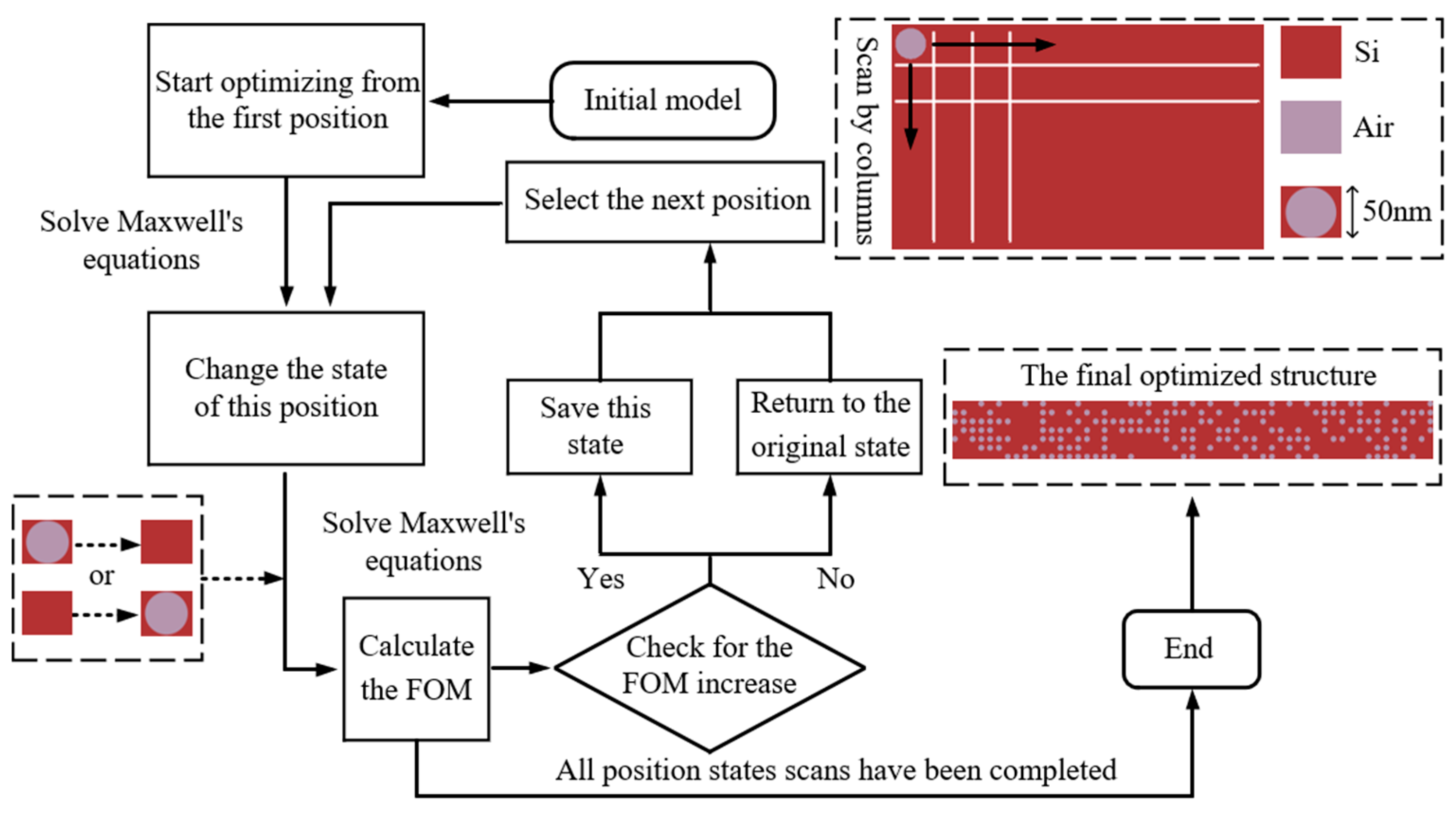
3.1. The Working Principle of DBS

Figure 5 and Algorithm 1 illustrate the working principle and the pseudocode flowchart of the inverse design based on the DBS algorithm, respectively. During the initial design phase, the footprint dimensions such as spacing, height, and ring radius are predefined. For electromagnetic field solutions, we implement 3D-FDTD simulations using the commercial software Lumerical 2024 R1 for transmission efficiency calculation, bandwidth calibration, and perfectly matched layer (PML) configuration. Before the process of DBS inverse design begins, a random matrix with a scale of 7 × 55 is generated to define the silicon unit states within the DBS regions. Next, the state of the first unit cell is toggled between silicon and air hole embedded states, followed by the recalculation of the electromagnetic field distribution where the newly obtained transmission efficiencies are input into the FOM. The updated FOM value is then compared to the previous FOM value. If the new FOM is larger, the unit state modification is retained, otherwise the cell reverts to its original state. The algorithm tests each pixel in order, starting with the first cell in column one. It repeats this testing pattern until all pixels in the coupling structure are complete.
Since the two rings in our device only have a slight difference in radius, we adopt the same size for the coupling area between each ring and the waveguide. Therefore, when establishing the FOM equation, we can determine whether the coupling structure has been adequately optimized by detecting the transmittance and reflectance of the single ring. According to the dual-ring transmission spectrum shown in Equation (17), we can obtain the theoretical transmission spectrum T ( ω 0 ) of a single ring at the resonant frequency ω 0 , which is expressed as follows:
T ( ω 0 ) = S 4 S + 1 2 = 4 γ w a v 2 ( 2 γ w a v + γ a ) 2 = 1 1 + γ a γ w a v + 1 4 γ a 2 γ w a v 2
In Equation (19), γ a denotes the transmittance of optical power loss, while γ w a v represents the transmittance of light coupled out of the ring. These parameters are measurable via monitors in Lumerical software as reflection R and transmittance T. Therefore, the equation of FOM is given as
F O M = 1 1 + R T + 1 4 R 2 T 2
As established in the theoretical analysis in Figure 4 in Section 2.3, the transmittance of the cascaded dual-ring system increases with a rising η value. This relationship corresponds to a decrease in γ a / γ w a v in Equation (19) and R / T in Equation (20), which causes the value of FOM to increase. Therefore, the physical interpretation of the FOM involves maximizing optical power transmission through the coupling structure between the ring and waveguide while minimizing reflection losses. Guided by this principle, the DBS inverse design optimizes the coupling structure of the dual-ring optical filter. During each iteration, our algorithm preserves structural changes when the FOM increases and advances the optimization. If the FOM decreases, the algorithm instantly reverts to the previous structure and tests the next pixel.
Algorithm 1. Direct Binary Search Method for Dual-Ring Filter Design
Photonics 12 00681 i001

3.2. Design of Dual-Ring Optical Filter

The diagram of the dual-ring optical filter structure designed in this paper is shown in Figure 6. The cascaded structure was constructed using the FDTD module in Lumerical software, comprising two rings with radii R 1 and R 2 of 4.8 μm and 5.7 μm, respectively, along with three waveguides. The width (W), thickness (H), and material of the waveguide and rings are 0.45 μm, 0.22 μm, and Si, respectively. The substrate material is SiO2 with a thickness, D, of 4 μm, and the distance between MRR-a and MRR-b is calculated using the following expression:
ϕ = β L L = ϕ β = ϕ λ 2 π n e f f
Equation (21) illustrates the relationship between phase ϕ and transmission distance L. n e f f 2.47 is the effective index of Si, and β is the propagation constant. Equation (16) demonstrates that the theoretical transmission achieves its maximum value of 1 when ϕ = ( m + 1 / 2 ) π (where m is a non-negative integer). We consider the reason for choosing the value of m as 41 from two aspects. Firstly, to avoid resonance caused by the close distance between the two rings, the distance L should be greater than the sum of R 1 and R 2 . Secondly, in order to ensure that there is sufficient optimized structure between the ring and the waveguide, the distance between the two rings along the x-axis should be greater than 8.2 μm. Therefore, according to Equations (16) and (21), the distance between MRR-a and MRR-b is set at 13 μm. The structural parameters are summarized in Table 1. From Figure 6a, it can be observed that the designed structure contains six ports. The light wave is input from Port 1 and output from Port 6. A monitor is placed at Port 1 to measure reflection, while another monitor is placed at Port 6 to measure transmittance. As established by Equation (14) in the theoretical analysis in Section 2, the coupling efficiency between the ring and waveguide serves as a critical factor influencing the total transmittance of the device. Therefore, four DBS design regions (two each on the upper and lower sides) have been implemented for both MRR-a and MRR-b. One of the DBS regions is illustrated in Figure 6b, consisting of a silicon slab measuring 8.2   μ m 2 . This region comprises 7 × 55 pixels arranged in a square lattice photonic crystal configuration. Each pixel is represented by a cylindrical structure with a 0.05 μm diameter, spaced 0.05 μm apart from adjacent cylinders. The binary encoding system (0 and 1) corresponds to two operational states. In state “1”, the cylindrical shape has a thickness of 0.22   μ m , with the material being air, which is displayed in white. In state “0”, the material is entirely silicon and is shown in red. Figure 7 illustrates the structural configurations of the four DBS regions in the dual-ring optical filter achieved through the DBS algorithm.

4. Numerical Calculations

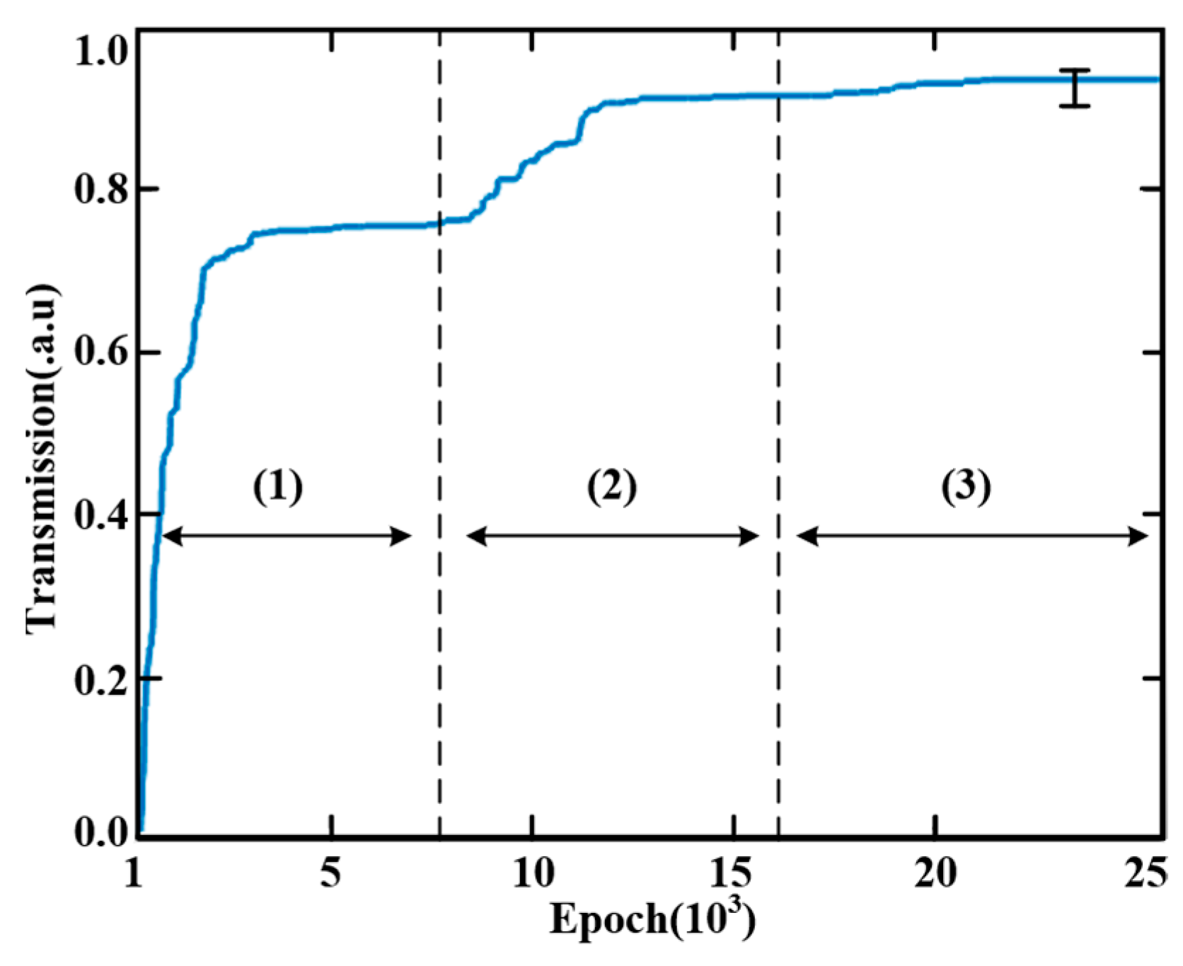
4.1. Optimization Based on DBS

During the inverse design process, the dual-ring optical filter underwent 25,000 iterations, with the transmission iteration relationship depicted in Figure 8. The optimization comprised three phases labeled (1), (2), and (3). In phase (1), only the DBS regions adjacent to the upper and lower sides of MRR-a were optimized while maintaining a 1   μ m default coupling gap between MRR-b and the waveguides. After 4000 iterations, the increasing trend of the transmittance slowed down, and the maximum transmittance was 0.72. Phase (2) began after 6000 iterations. Phase (2) initiated the optimization of the DBS regions adjacent to both sides of MRR-b, building upon the preserved structure of phase (1). A significant improvement in transmittance was observed during approximately the 6000th to 11,800th iterations. When transmittance reached 0.91, the optimization effect approached saturation. Phase (2) entered its final stage at 16,250th iterations. Phase (3) performed random scans across all four DBS regions of the structure derived in phase (2). Figure 8 reveals small transmission gains in the device during iterations 16,250 to 21,000. Upon reaching the maximum transmittance of 0.93, transmission stabilized with negligible further variation. The inverse design process terminated after 25,000 iterations. The transmission error shown by the error bars in Figure 8 is approximately 7%. Device loss variations at a temperature range of 295–305 K contribute about 2%, while simulation software limitations (primarily from the mesh resolution settings) account for the remaining 5%.

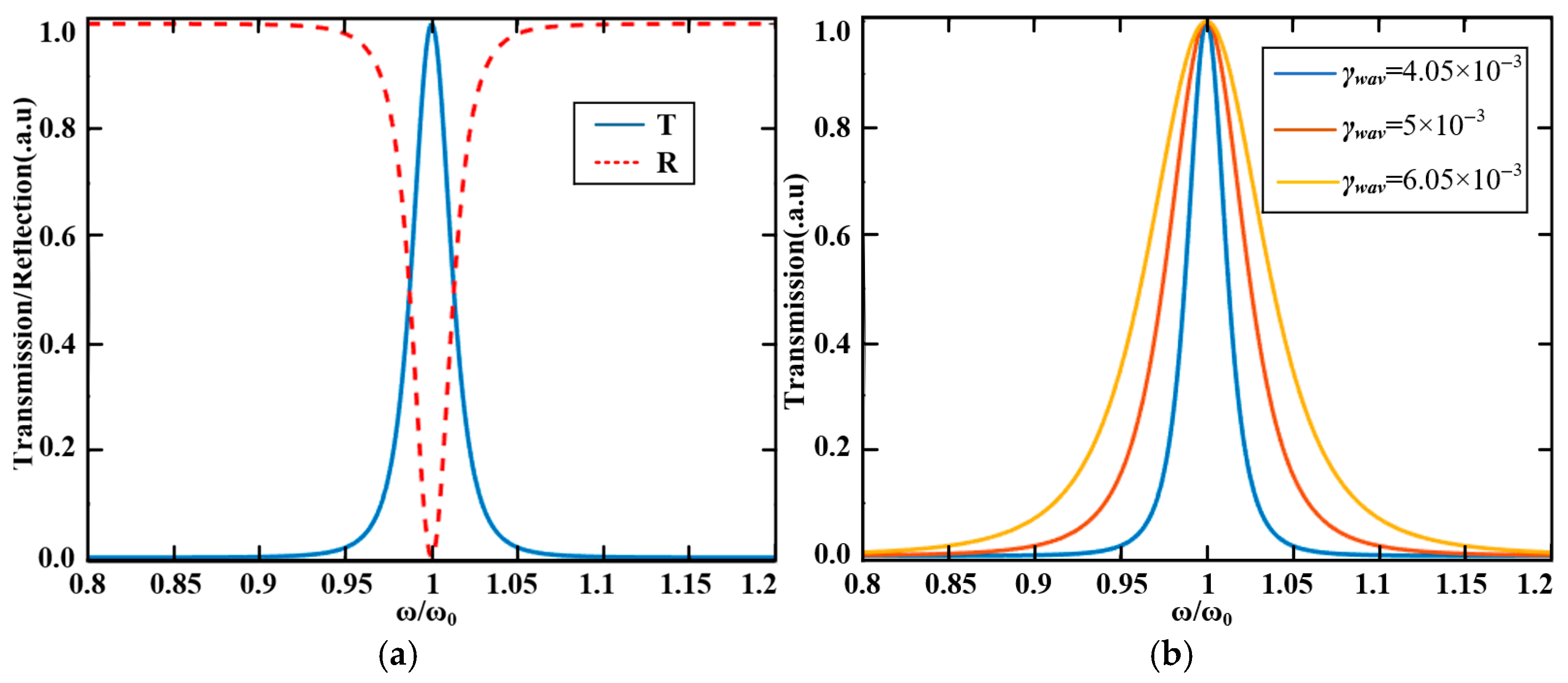
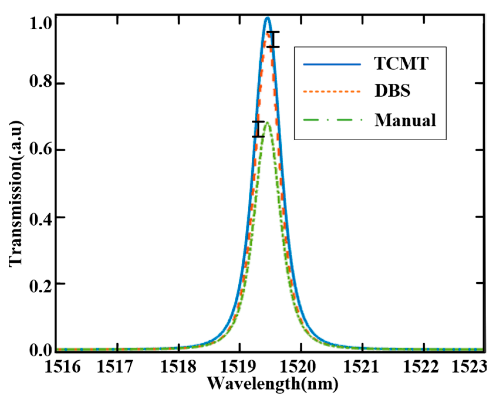
4.2. Transmission Spectra

Based on the four DBS regions mentioned above, FDTD simulations were performed to characterize the transmission spectra of the dual-ring optical filter across the 1480 to 1650 nm input wavelength range. Figure 9a compares the resonant peaks of MRR-a and MRR-b, revealing different FSR values due to radius mismatch. Coincident resonant peaks occur at 1519.5 nm and 1605.5 nm, while the remaining peaks exhibit spectral offset. The proposed device’s transmission spectrum is shown in Figure 9b, which demonstrates an 86 nm FSR, a 0.3 nm linewidth, a 0.3 dB insertion loss, and an approximately 22 dB extinction ratio.
The transmission spectra comparison between TCMT and the DBS algorithm is shown in Figure 10. The blue curve denotes the theoretical spectrum derived from TCMT (Equation (16)), while the orange dashed line represents the FDTD-simulated spectrum assisted by the DBS algorithm. The green dotted line corresponds to the conventional manual design. At the operational wavelength of 1519.5 nm, the peak transmittance values of TCMT, DBS, and manual design are 1, 0.93, and 0.69, respectively. The superior theoretical performance arises from two factors: (1) the idealized lossless MRR assumption ( γ a = γ b = 0 ) in the TCMT derivation and (2) FDTD’s comprehensive loss modeling incorporating waveguide propagation loss, ring bend radiation, and out-of-plane (z-axis) structural dissipation. In addition, the trend of the theoretical transmission spectrum derived based on TCMT is basically consistent with that obtained by the DBS algorithm, while the transmission efficiency of the devices designed manually is significantly lower.

4.3. Steady-State Field Distribution

Figure 11a–d display the steady-state field distributions when optical waves with wavelengths of 1519.5 nm, 1519 nm, 1536 nm, and 1533 nm, respectively, are seen in Port 1. As analyzed earlier, since the resonance peaks of MRR-a and MRR-b coincide at 1519.5 nm, Figure 11a demonstrates that the input optical wave with a wavelength of 1519.5 nm is nearly fully sequentially coupled into MRR-a and MRR-b, ultimately outputting from Port 6 with no reflected intensity at Port 1. This phenomenon occurs because the optical energy propagates unidirectionally within the MRR, forming resonance peaks through periodic cycling, which known as traveling wave resonance, thereby preventing backward propagation to the input at Port 1. When the wavelength of input light approaches the resonant wavelength of the MRR, as shown in Figure 11b, only a portion of the light intensity at the 1519 nm wavelength is coupled into the two MRRs. Meanwhile, a significant amount of light intensity is reflected back at Port 1. This occurs because the wavelength mismatch causes partial light intensity to generate standing wave resonance between the MRR and waveguide, which subsequently reflects back. Consequently, this light cannot ultimately propagate to Port 6. When the input light wavelength is 1536 nm, as shown in Figure 11c, the input wavelength matches the resonant wavelength of MRR-a. Consequently, most of the optical power is coupled into MRR-a and further transferred to the bus waveguide. However, when the light reaches MRR-b, its wavelength no longer aligns with the resonant wavelength of this resonator. As a result, the light is reflected and fails to propagate to Port 6. When the incident light wavelength is 1533 nm, as shown in Figure 11d, the input light wavelength coincides with the resonant wavelength of MRR-b but not with that of MRR-a. Consequently, the light wave is reflected upon reaching MRR-a during transmission, resulting in the detection of a large reflection at Port 1.

4.4. The Fabrication Tolerance of the Device

The structural dimension deviations are complex problems, and the size deviations of the air holes ( r h o l e s ) in the coupling structure and the radius of the rings ( r M R R ) have a significant impact on the performance of the designed device. In addition, temperature fluctuations (t) will also have a certain impact on the insertion loss of the proposed dual-ring filter. Therefore, we investigated the effect of the size deviations of r h o l e s and r M R R and the temperature fluctuations of t, respectively.
(1)
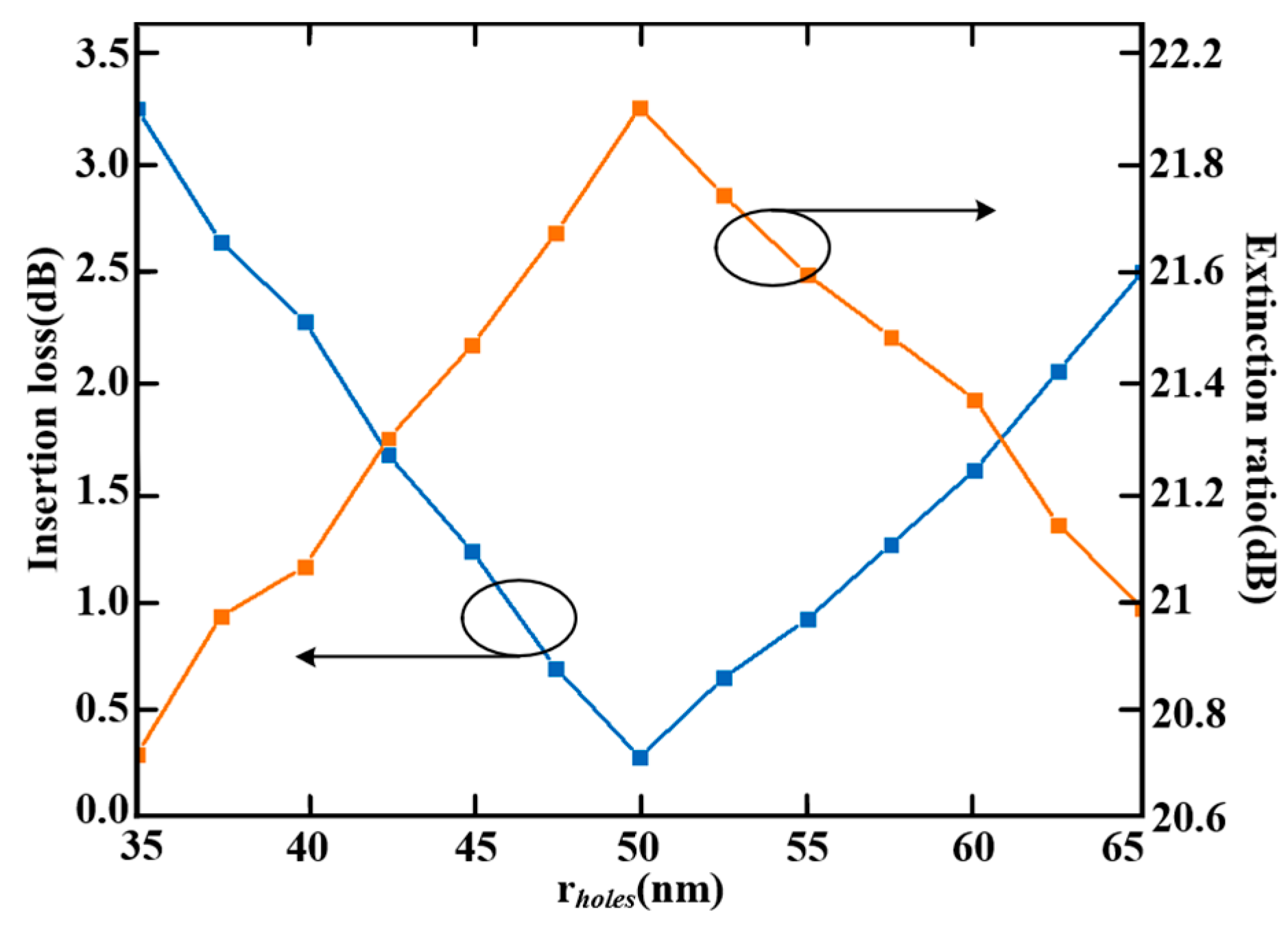
The radius of air holes in the coupling structure is r h o l e s = 50   nm . We changed the value of r h o l e s to observe its influence on the device’s performance. From Figure 12, we can observe that the change in r h o l e s has a great influence on the insertion loss and extinction ratio of the device. Better performance (transmittance ≥ 80%) can be achieved when the air holes’ radius of r h o l e s is changed from 45.8 nm to 57.2 nm. Otherwise, the transmission efficiency of the device will decrease due to the weak coupling coefficient between rings and waveguides. When r h o l e s = 50   nm , the insertion loss reaches the lowest point. Hence, the fabrication tolerance range for air holes (diameter) in the coupling structure is 22.8 nm.
(2)
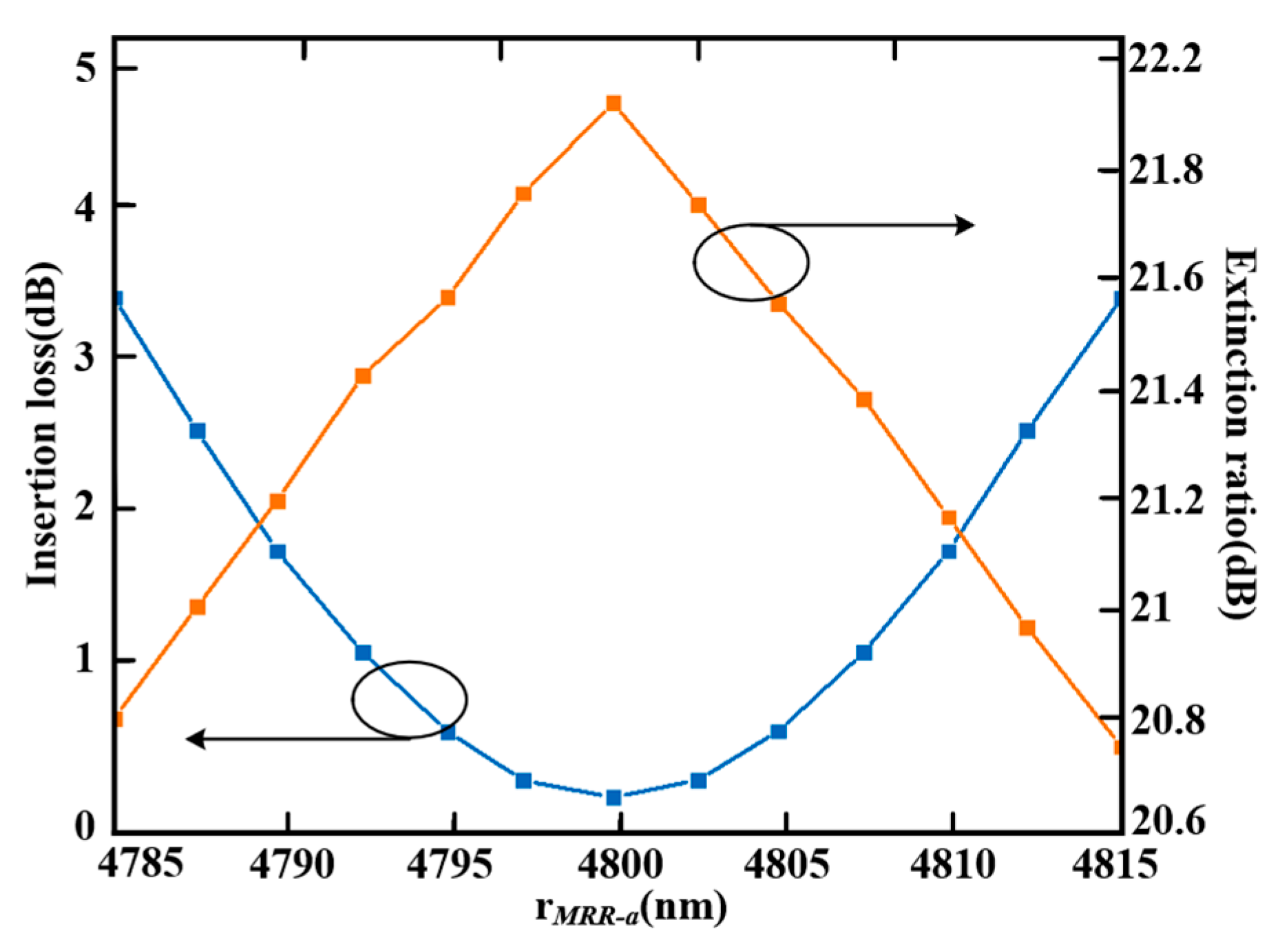
The radii of the rings in our proposed dual-ring filter are r M R R a = 4800   nm and r M R R b = 5700   nm , respectively. Since changing the radius of either MRR-a or MRR-b will cause mismatch in the resonant wavelength, we changed the value of r M R R a to observe its influence on the device’s performance. From Figure 13, we can observe that the change in r M R R a has a great impact on the insertion loss and extinction ratio of the proposed device. Transmittance can exceed 80% when r M R R a is between 4792.8 nm and 4807.3 nm. However, as the radius perturbation of MRR-a increases, the insertion loss of the device will increase due to the mismatch between the primary resonant peaks of MRR-a and MRR-b. Therefore, the fabrication tolerance for the radius r M R R a is 14.5 nm.
(3)
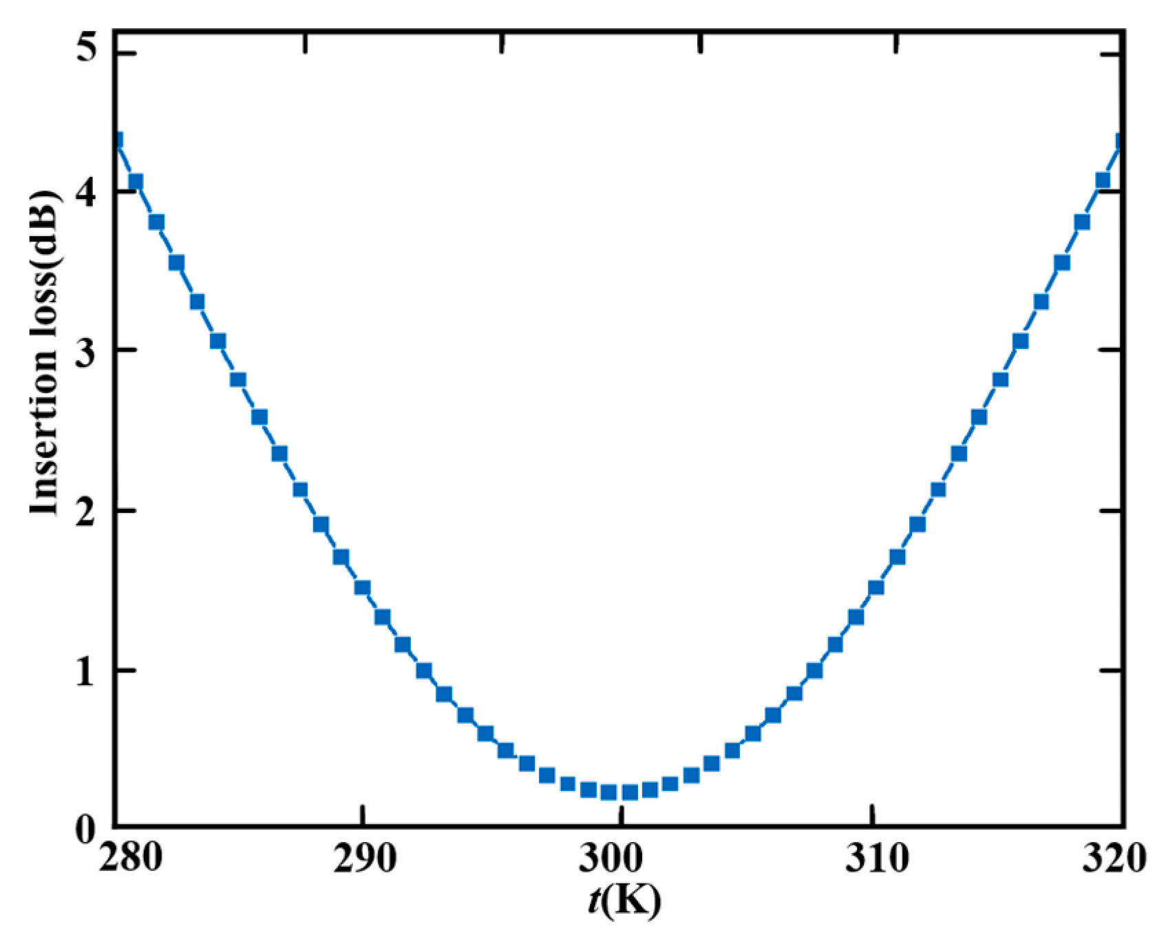
When analyzing the impact of temperature fluctuations t on device performance, we employed a step of 0.8 K to simulate the temperature change. We utilized the “DEVICE” and “Interconnect” modules in Lumerical software to calculate the insertion loss of the device at temperatures ranging from 280 K to 320 K. When the temperature of silicon changes, the refractive index changes. This causes the resonant peaks of the rings to shift and affects the maximum transmittance. From Figure 14, we can observe that the change in temperature t has relatively little effect on the insertion loss of the device considering the transmittance is higher than 90% when t is between 295 K and 305 K. However, the insertion loss will increase significantly if the temperature variation becomes greater. This is because the temperature fluctuations causes a change in the effective refractive index of the silicon material. Furthermore, the resonant peak of the ring has shifted, and it is unable to confine the light wave at the operation wavelength. Therefore, the temperature tolerance range of the proposed device is from 295 K to 305 K.

5. Discussion

Performance comparisons of the devices that were designed using manual and DBS methods are summarized in Table 2. As shown in Table 2, most devices designed manually have disadvantages in terms of insertion loss [14,15,25,26]. This is because such approaches consider limited structural parameters while neglecting some details, such as the coupling efficiency, which might cause losses. However, the manual method offers certain design flexibility. As shown in reference [27], the device structure sacrifices the FSR in exchange for lower loss and a narrow linewidth by manually optimizing the quality factor of the photonic crystal nano-ring. The designed photonic devices assisted by the DBS algorithm exhibit a common advantage with low insertion loss, as shown in Table 2. Through continuous nanostructure iteration, lower losses are achievable while maintaining a relatively compact size.
This work significantly expands the FSR compared to other dual-ring structures [15,25,26,27]. Using the Vernier effect to achieve a large FSR requires slightly different sized rings and avoids excessively small dimensions to preserve resonant peak density. Larger device dimensions increase transmission loss, which is an inevitable fundamental trade-off for the proposed dual-ring optical filter. However, our theoretical analysis of the dual-ring optical filter based on TCMT revealed how its light transmission efficiency depends on the coupling attenuation coefficient between rings and waveguides. Using this key relationship, we designed a device with a relatively compact 24 × 25.5   μ m 2 footprint, simultaneously employing the DBS algorithm to minimize insertion loss. Furthermore, the dual-ring structure based on the Vernier effect also has a larger FSR compared with other multi-mode interference structures [21,22,23]. The proposed device exhibits an insertion loss, extinction ratio, FSR, and linewidth of 0.3 dB, 22 dB, 86 nm, and 0.3 mn, respectively, which are superior to current studies, as shown in Table 2.
Based on our current findings, some promising research directions can be proposed. Firstly, the Si waveguide in our dual-ring optical filter can be replaced with Si3N4 waveguides, which have the advantages of a higher refractive index with low transmission loss. Secondly, a third high-quality ring resonator can be cascaded to achieve a narrower linewidth. Thirdly, the designed dual-ring structure can be used as an external cavity in laser devices for coherent optical communication. This is because the external cavity can significantly increase the cavity length of the laser, resulting in a narrower output linewidth. Finally, the designed device’s narrow linewidth, high extinction ratio, and large FSR enable resonant wavelength tuning via integrated heaters for dense wavelength division multiplexing.
Table 2. Performance comparison.
ReferenceMethodInsertion Loss (dB)Extinction Ratio (dB)FSR (nm) Footprint   ( μ m 2 ) Line Width (nm)
[25]Manual2.211.5354750.4
[27]Manual0.3625.077.8 23.8 × 20.82 0.5
[15]Manual18.55.815.76-10
[26]Manual5.6139-1
[14]Manual15.7872-0.62
[20]DBS0.8616.870 42 × 6.8 -
[21]DBS0.75910.0650 2.4 × 3.6 -
[22]DBS0.52040 3 × 4 -
[23]DBS0.8218.135 3.6 × 2.4 2
This workDBS0.32286 24 × 25.5 0.3

6. Conclusions

This study presents a theoretical model of a cascaded dual-ring structure based on the TCMT and conducts a theoretical analysis, deriving a theoretical result of maximum transmittance reaching 1. By analyzing the theoretical transmission spectrum, it is concluded that the coupling efficiency between the ring and the waveguide is the core structure that affects the transmission efficiency of the dual-ring optical filter. Furthermore, the theoretical equation is utilized to establish the FOM as the performance indicator for optimizing the coupling structure in the DBS algorithm. The transmission performance was calculated by using the 3D-FDTD method. The device exhibits low insertion loss and high extinction ratio and FSR, along with a compact size and narrow linewidth. The constructed DBS algorithm significantly enhances device performance. Our methodology combines TCMT with the DBS algorithm, establishing a new design paradigm for complex photonic devices. The proposed device can be applied as a laser external cavity in the coherent optical communication field, and its narrow linewidth, large extinction ratio, and FSR show significant potential for DWDM systems.

Author Contributions

Conceptualization, Y.H.; Methodology, Y.H.; Software, Y.H.; Validation, Y.H.; Formal analysis, Y.H.; Investigation, T.W.; Resources, T.W.; Data curation, T.W.; Writing—original draft, Y.H.; Supervision, B.H.; Project administration, W.Z. and B.H.; Funding acquisition, W.Z. All authors have read and agreed to the published version of the manuscript.

Funding

This research was funded by the National Natural Science Foundation of China (No. U24B20168).

Institutional Review Board Statement

Not applicable.

Informed Consent Statement

Not applicable.

Data Availability Statement

No new data were created in the present research.

Conflicts of Interest

The authors declare no conflicts of interest.

References

  1. Wang, L.; Wang, X.; Pan, S. Microwave Photonics Empowered Integrated Sensing and Communication for 6G. IEEE Trans. Microw. Theory Tech. 2025, 1–21. [Google Scholar] [CrossRef]
  2. Ma, W.; Wang, R.; Liu, J.; Li, W. High-Performance Integrated Microwave Photonic Transceiver for Dual-Band Synthetic Aperture Radar. J. Light. Technol. 2024, 42, 7482–7490. [Google Scholar] [CrossRef]
  3. Tian, X.; Li, L.; Nguyen, L.; Yi, X. Integrated Microwave Photonic Sensors Based on Microresonators. Adv. Sens. Res. 2024, 3, 2300145. [Google Scholar] [CrossRef]
  4. Liu, F.; Tang, Z.; Wu, R.; Tang, L.; Van Thourhout, D.; Pan, S. Silicon Integrated Microwave Photonic Mixer Based on Cascaded ring Resonator Modulators. IEEE Photonics Technol. Lett. 2024, 36, 333–336. [Google Scholar] [CrossRef]
  5. Qin, X.; Shi, T.; Wang, Z.; Shi, H.; Chen, J. Research progress of narrow-linewidth external cavity diode lasers. Instrumentation 2024, 45, 63–78. [Google Scholar]
  6. Mala, A.; Mandal, S. Modelling and performance analysis of cascaded asymmetrical quadruple micro-optical ring resonator as an optical filter. Opt. Quant. Electron. 2023, 55, 969–994. [Google Scholar] [CrossRef]
  7. Foroughifar, A.; Saghaei, H.; Veisi, E. Design and analysis of a novel four-channel optical filter using ring resonators and line defects in photonic crystal microstructure. Opt. Quant. Electron. 2021, 53, 101–113. [Google Scholar] [CrossRef]
  8. Qasrawi, A.F. Thickness-Controlled Ti Optical Filters Designed for Tunable Terahertz Technology. Phy. Status Solidi B 2025, 262, 2400648. [Google Scholar] [CrossRef]
  9. Huang, Y.; Li, Y.; Zhu, H.; Tong, G.; Zhang, H.; Zhang, W.; Zhou, S.; Sun, R.; Zhang, Y.; Li, L.; et al. Theoretical investigation into spectral characteristics of a semiconductor laser with dual-FBG external cavity. Opt. Commun. 2011, 284, 2960–2965. [Google Scholar] [CrossRef]
  10. Wei, J.; Zhu, C.; Yu, Y.; Wang, R.; Yu, S. Low-loss silicon waveguide and an ultrahigh-Q silicon ring resonator in the 2 µm wave band. Opt. Lett. 2024, 49, 3271–3274. [Google Scholar] [CrossRef]
  11. Ma, X.X.; Zhao, Y.; Yao, H.; Deng, J.Y.; Wu, J.Y.; Hu, Z.F.; Chen, K.X. Compact and Highly Sensitive Refractive Index Sensor Based on Embedded Double-Ring Resonator Using Vernier Effect. IEEE Photonics J. 2023, 15, 1–9. [Google Scholar] [CrossRef]
  12. Guo, Y.; Li, X.; Jin, M.; Lu, L.; Xie, J.; Chen, J.; Zhou, L. Hybrid integrated external cavity laser with a 172-nm tuning range. APL Photonics 2022, 7, 066101–066109. [Google Scholar] [CrossRef]
  13. Calo, C.; Benyahya, K.; Mardoyan, H.; Charbonnier, P.; Sacchetto, D.; Zervas, M.; Mekhazni, K.; Lanteri, D.; Gariah, H.; Fortin, C.; et al. Hybrid InP-SiN microring-resonator based tunable laser with high output power and narrow linewidth for high capacity coherent systems. In Proceedings of the 2022 Optical Fiber Communications Conference and Exhibition (OFC), San Diego, CA, USA, 6–10 March 2022; pp. 1–3. [Google Scholar]
  14. Lin, T.; Lu, F.; Zhou, P.; Chen, Y.; Jiang, J.; Hu, G.; Yun, B.; Cui, Y. Ultrabroadband vernier cascaded microring filters based on dispersive Si3N4 waveguides. J. Opt. 2024, 26, 025802. [Google Scholar] [CrossRef]
  15. Yang, L.; Dong, B.; Shao, Q.; Zhang, S.; Chen, Z. Short Carbon Nanotube Nano-Film-Based Polymer/SiO2 Hybrid Waveguide Micro-Ring Filter. ACS Appl. Mater. Interfaces 2023, 15, 28555–28562. [Google Scholar] [CrossRef] [PubMed]
  16. Bhai, R.K.C.; Flagg, E.B. Narrow-bandwidth tunable optical filter stabilized by Newton’s rings fringe analysis. Appl. Opt. 2024, 63, 3117–3122. [Google Scholar]
  17. Stratakis, I.; Avraam, C.; Kastritsis, D. Ultra-narrowband dual-cavity Bragg grating ring resonator optical filter. Opt. Commun. 2025, 577, 131330. [Google Scholar] [CrossRef]
  18. Molesky, S.; Lin, Z.; Piggott, A.Y. Inverse design in nanophotonics. Nat. Photonics 2018, 12, 659–670. [Google Scholar] [CrossRef]
  19. Shen, B.; Wang, P.; Polson, R. An integrated-nanophotonics polarization beamsplitter with 2.4 × 2.4 μm2 footprint. Nat. Photonics 2015, 9, 378–382. [Google Scholar] [CrossRef]
  20. Lin, J.; Wang, P.; Fu, Q.; Chen, W.; Dai, S.; Kong, D.; Chen, H.; Li, J.; Dai, T.; Yang, J. Low-loss and broadband polarization-insensitive high-order mode pass filter based on photonic crystal and tapered coupler. Opt. Lett. 2023, 48, 3347–3350. [Google Scholar] [CrossRef]
  21. Wang, Z.; Li, Z.; Hou, X.; Zhang, J. Reverse design of multifunctional demultiplexing devices. Photonics Nanostruct. 2024, 58, 101246. [Google Scholar] [CrossRef]
  22. Zhou, S.; Wang, Z.; Nong, J.; Li, H.; Du, T.; Ma, H.; Li, S.; Deng, Y.; Zhao, F.; Zhang, Z.; et al. Optimized wideband and compact multifunctional photonic device based on Sb2S3 phase change material. Opt. Express 2024, 32, 8506–8519. [Google Scholar] [CrossRef]
  23. Yuan, H.; Huang, J.; Wang, Z.; Zhang, J.; Deng, Y.; Lin, G.; Wu, J.; Yang, J. An ultra-compact dual-channel multimode wavelength demultiplexer based on inverse design. Results Phys. 2021, 27, 104489. [Google Scholar] [CrossRef]
  24. Ma, H.; He, X.; Zhu, G. Different-mode power splitters based on a multi-dimension direct-binary-search algorithm. Opt. Express 2023, 31, 27393–27406. [Google Scholar] [CrossRef] [PubMed]
  25. Babu, D.L.; Sreenivasulu, T. 4-Channel DWDM demultiplexer on silicon photonic crystal slab. Sadhana 2021, 46, 14. [Google Scholar] [CrossRef]
  26. Cassese, T.; Giambra, M.A.; Sorianello, V.; De Angelis, G.; Midrio, M.; Pantouvaki, M.; Van Campenhout, J.; Asselberghs, I.; Huyghebaert, C.; D’Errico, A.; et al. Capacitive actuation and switching of add–drop graphene-silicon micro-ring filters. Photonics Res. 2017, 5, 762–766. [Google Scholar] [CrossRef]
  27. Delphi, G.; Olyaee, S.; Seifouri, M.; Mohebzadeh-Bahabady, A. Design of low cross-talk and high-quality-factor 2-channel and 4-channel optical demultiplexers based on photonic crystal nano-ring resonator. Photonic Netw. Commun. 2019, 38, 250–257. [Google Scholar] [CrossRef]
Figure 1. Theoretical model of dual-ring optical filter.
Photonics 12 00681 g001
Figure 2. The relationship between numerical value and γ w a v a / γ a .
Photonics 12 00681 g002
Figure 3. The relationship between transmittance and frequency detuning of the cascaded dual-micro-ring system: (a) the spectrum of transmission and reflection; (b) different amplitude attenuation coefficients.
Photonics 12 00681 g003
Figure 4. The variation in the attenuation coefficient ratio versus transmittance in a cascaded dual-ring system.
Photonics 12 00681 g004
Figure 5. The working principle of DBS inverse design.
Photonics 12 00681 g005
Figure 6. Dual-ring optical filter structure diagram: (a) 3D structure; (b) DBS region.
Photonics 12 00681 g006
Figure 7. Structural configurations of the four DBS regions.
Photonics 12 00681 g007
Figure 8. Transmittance variation with number of iterations: (1) Phase one, (2) Phase two, (3) Phase three.
Photonics 12 00681 g008
Figure 9. Transmission spectra at wavelength range of 1480 nm to 1650 nm. (a) Comparison of resonance peaks. (b) Transmission spectra of proposed device.
Photonics 12 00681 g009
Figure 10. Comparison of theoretical and simulated transmission spectra.
Photonics 12 00681 g010
Figure 11. Steady-state field distribution at different operating wavelengths: (a) 1519.5 nm; (b) 1519 nm; (c) 1536 nm; and (d) 1533 nm.
Photonics 12 00681 g011
Figure 12. Insertion loss (blue line) and extinction ratio (orange line) versus radius of air holes r h o l e s .
Photonics 12 00681 g012
Figure 13. Insertion loss (blue line) and extinction ratio (orange line) versus radius of MRR-a.
Photonics 12 00681 g013
Figure 14. The relationship between insertion loss and temperature t.
Photonics 12 00681 g014
Table 1. Structural parameters.
ParameterValueParameterValue
R 1 4.8   μ m W w g 0.45   μ m
R 2 5.7   μ m H w g 0.22   μ m
d 13   μ m W M R R 0.5   μ m
DBS region 8.2   μ m 2 H M R R 0.22   μ m
Footprint 24   μ m × 25.5   μ m D 4   μ m
Disclaimer/Publisher’s Note: The statements, opinions and data contained in all publications are solely those of the individual author(s) and contributor(s) and not of MDPI and/or the editor(s). MDPI and/or the editor(s) disclaim responsibility for any injury to people or property resulting from any ideas, methods, instructions or products referred to in the content.

