1. Introduction
The third-generation semiconductor materials, gallium nitride (GaN) and silicon carbide (SiC), are increasingly becoming key materials for high-power and high-frequency electronic devices due to their physical properties, such as wide forbidden bands, high breakdown electric fields, and excellent thermal conductivity [
1,
2]. In high-voltage and high-frequency application scenarios [
3], these materials exhibit far better overall performance than traditional silicon materials. With the rapid development of electrified and intelligent vehicles, the market demand for in-vehicle smart chips and power semiconductors continues to grow, further driving the technological evolution of third-generation semiconductor materials. However, its manufacturing process still faces multiple challenges, including high manufacturing cost, difficult crystal quality control, significant wafer warpage and bending problems, harsh surface roughness requirements, susceptibility to cracking, narrow epitaxial growth window [
4], and susceptibility to particle contamination, among other challenges [
5,
6]. Among them, key geometrical parameters, such as wafer warpage, flatness, and thickness [
7,
8,
9], have a decisive impact on the controllability of subsequent processes and device performance. Silicon carbide and silicon-based wafers are highly susceptible to deformation during the manufacturing process, which significantly increases the process difficulty of subsequent grinding, polishing, and encapsulation, and thus reduces the consistency and yield of the finished product [
8]. Therefore, realizing the high-precision measurement of morphological parameters, such as wafer warpage and thickness, has become one of the key technical bottlenecks in the third-generation semiconductor manufacturing process.
Non-contact techniques are commonly used for wafer thickness inspection to avoid microscopic damage to the surface caused by contact probes [
10]. The current mainstream solutions include spectral confocal, thin-film interferometry, laser interferometry, white-light vertical scanning interferometry (CSI), and deflectometry measurement [
11,
12]. Spectral confocal sensors can achieve submicron resolution with axial chromatic aberration compensation, but due to their shot-point architecture limited by spot diameter, they can only be acquired at discrete points, resulting in insufficient sampling density and limited coverage of a single measurement [
13]. Thin-film interferometers are based on Fabry–Pérot interferometric cavities, which have nanometer-scale repeatability but require ≥ 90% reflectivity of the measured surface; on SiC/Si thin films, the problems of Fresnel reflections and low signal-to-noise ratios, as well as the inefficiency of point-by-point measurements, constrain their application [
14]. Laser interferometry (e.g., Zygo Verifire
TM XL) can achieve
flatness accuracy through wavefront phase reconstruction, but is limited by the coherence length [
15], and can only obtain the upper surface 3D topography; for double-sided polished and semi-transparent SiC substrates, multiple reflections on the upper and lower surfaces result in overlapping fringes, which further reduces the deciphering robustness [
16]. The CSI technique utilizes a broadband white light source to suppress harmonic interference, thus achieving submicron resolution in the axial direction; however, the field of view is small, the measurement efficiency is limited, and the pseudo-peak signals are prone to appear on SiC wafers with an epitaxial layer, which affects the facet reconstruction [
17]. The stripe deflection method reconstructs the full-field surface height by projecting known stripes and capturing their reflective deformations, which has the advantages of high accuracy and non-contact, but the solution is still difficult for the task of acquiring the upper and lower surfaces at the same time and extrapolating the thickness.
By contrast, frequency scanning interferometry (FSI) has become the preferred method for wafer flatness and thickness inspection due to its full-field, high-speed, high-precision, and multilayer measurement capabilities. FSI obtains the interference phase in real time by precisely tuning the wavelength of the light source during the scanning process, and reconstructs the upper and lower surface topography and thickness variations (TTV) [
18]. The result is a comprehensive evaluation of key geometrical parameters, such as flatness and warpage, which meets the stringent requirements of third-generation semiconductor manufacturing for efficient, non-contact, and full-field measurements.
In wavelength-tuned interferometry, multi-surface reflections from Si/SiC wafers cause harmonic aliasing and crosstalk, severely impacting surface pattern accuracy. These effects are exacerbated by high refractive index materials, multiple reflection paths, and warp-induced thickness gradients, leading to frequency modulation distortion and significant interference errors in SiC wafer fringes due to brittle defects [
19]. To address these challenges, the excess fraction method combines piezoelectric ceramic (PZT)-driven phase modulation with wavelength scanning to compensate for nonlinear errors through correlation integrals, suppressing periodic hopping errors to 12 nm but still exhibiting a residual error of 0.1λ due to PZT hysteresis [
19,
20]. The 6N-5 algorithm employs Legendre orthogonal polynomials to filter out fifth-order nonlinear terms, reducing optical thickness measurement uncertainty in BK7 glass from 5.6 nm to 1.8 nm, though its side-flap attenuation remains limited [
21,
22]. For highly reflective surfaces, the 10N-9 phase-shift algorithm integrates discrete Fourier transform with a polynomial window function to achieve an 18 dB reduction in higher-order reflective noise power and control reproducibility error to 2.045 nm in silicon wafer topography inspection [
22]. In frequency-scanning interferometry, frequency stepping interferometry generates synthetic wavelengths via discrete tuning, combined with generalized Fourier transform to achieve submicron optical range resolution. This technique achieves 0.78 μm parallelism accuracy over a 150 mm field of view but suffers from up to 3.2% spectral leakage error [
21]. The improved MST interferometer separates multiple reflected signals from thin wafers through wavelength scanning, yet its adaptability to high refractive index materials is limited by the Brewster angle effect [
23]. Iterative optimization methods, such as the harmonic stripe iterative method, improve computational efficiency by three times while reducing morphology solution error by 50%, and the enhanced phase iteration algorithm reduces ripple error from 12.5 nm to 5.1 nm by optimizing the Jacobi matrix condition number. For multi-surface signal processing, the frequency-domain separation method controls BK7 plate surface topography PV error within 1.0 μm by increasing spectral spacing [
24]. The 3N-2 phase-shifting algorithm suppresses multiple-reflection fringe noise in lithium niobate crystals from 30% to 1%, but its anti-vibration performance is limited by a phase jitter threshold of λ/20 [
25]. The conventional least-squares iterative method faces three core challenges in resolving the dual-surface topography of the Si/SiC thin films complicating model fitting, including higher-order harmonic aliasing due to multi-interface reflections and spectral overlap, reflectivity asymmetry between the surfaces causing uneven interference intensity and the Jacobi matrix pathology, and refractive index modulation from non-uniform doping gradients [
17].
In this paper, a frequency scanning interferometry experimental system based on the Fizeau interferometric optical path is firstly constructed for the precise measurement of flatness and thickness variation of semiconductor thin films. The system makes full use of the advantages of the near-infrared wavelength band in the penetration of Si and SiC wafers, adopts a common optical path design to reduce the optical path error, and realizes step-triggered acquisition and precise phase regulation through wavelength conversion during the scanning process. In addition, the proposed “oversampling” technique significantly enhances the ability of extracting weak interference signals from multilayer structures, which provides strong support for subsequent signal separation and reconstruction. In order to solve the problems of harmonic aliasing, matrix pathology and nonlinear phase modulation in the interferometric solution of multilayer surfaces, a high-precision surface reconstruction algorithm is proposed in this paper to suppress the multiple harmonics of the SiC/Si wafer. The algorithm integrates the harmonic spectral domain decomposition, refractive index gradient physical constraints and partition optimization strategy to systematically improve the deconstruction accuracy, which enables the simultaneous reconstruction of the upper and lower wafer surface information and thickness variations, and realizes the comprehensive evaluation of the wafer flatness, warpage, and thickness variations.
2. Principles and Models
When the frequency scanning interferometry (FSI) technique is used to measure the 3D topography of parallel flat plates, the accurate recovery of phase information is the key to realize high-precision reconstruction. In order to deeply analyze the influence of the interference effect of multiple reflected beams on the phase extraction accuracy [
26], a set of simulation experiments based on the superposition of mixed interferometric signals is designed and implemented in this paper. As shown in
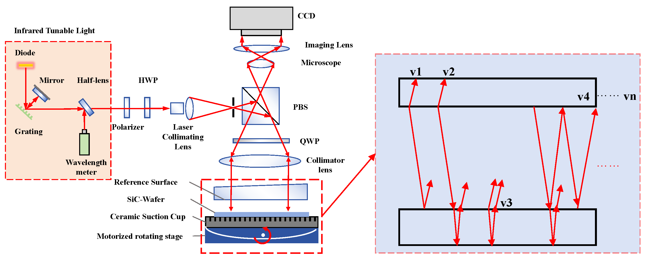
Figure 1, the HWP (half-wave plate) rotates the polarization direction of linearly polarized light by introducing a half-wavelength phase difference, while the QWP (quarter-wave plate) converts linearly polarized light into circularly polarized light by adding a quarter-wavelength phase shift, and the PBS (polarization beam splitter) separates the light beam according to polarization, transmitting one polarization state while reflecting the other. The light source is continuously wavelength tuned. These components reflect different contributions to the overall interference pattern and are essential for accurate analysis. The HWP and QWP manipulate light polarization to optimize beam propagation and minimize reflection losses, while the PBS directs polarized light for precise interferometric measurements, and the laser collimating lens ensures high-resolution imaging by focusing the sample beam in the FSI system.
By numerically simulating the combination of interferometric signals with different reflection paths, the stability and robustness of typical phase recovery algorithms in complex interferometric environments are systematically evaluated and their optimization directions are explored [
27]. During the simulation, the mixed interferometric signals are modeled as a superposition of coherent beams generated by reflections from multiple interfaces. Specifically, when the incident light is irradiated to a parallel flat plate, the multiple reflections formed between the front and back surfaces will generate two or more coherent light beams, which interfere with each other inside the interferometer, and ultimately form an interferogram pattern with typical characteristics on the detector. For any pixel in the interferogram, the interfering light intensity can be expressed as a vectorial superposition of the reflected beams, which needs to take into account factors such as optical range difference, phase difference, and amplitude distribution. Through the fine modeling and simulation calculation of the above process, the interferograms are generated with high consistency with the actual measurement conditions, which provide the theoretical basis and data support for the construction of the subsequent experimental system and the optimization of the phase solving algorithm.
where
is the frequency of light intensity change of the interference signal. For multi-surface interference, the frequency of change of light intensity of the interference signal formed by each surface can be written as follows:
where
and
denote the number of reflections between the reference mirror and the test mirror, and within the flat plate, respectively,
is the refractive index at wavelength
is the thickness of the flat plate, and
represents the rate of change of the refractive index with wavelength. The values of
and
correspond to the frequencies of interference formed between the front surface, rear surface of the parallel plate, and the optical thickness variation of the plate, respectively.
where
represent the parasitic signals generated by the remaining multiple reflections in addition to the three surfaces interfering with each other. Under the condition that the refractive index of each point of the parallel plate to be tested is the same, the relative amplitude and frequency distribution of each interference signal are shown in
Table 1.
On the basis of the above double-surface interferometry simulation, and also to ensure the simulation effect, control
,
,
= 1.5 × 10
−13, and the number of simulation images is 1000. The simulation results are shown in
Figure 2 and
Figure 3.
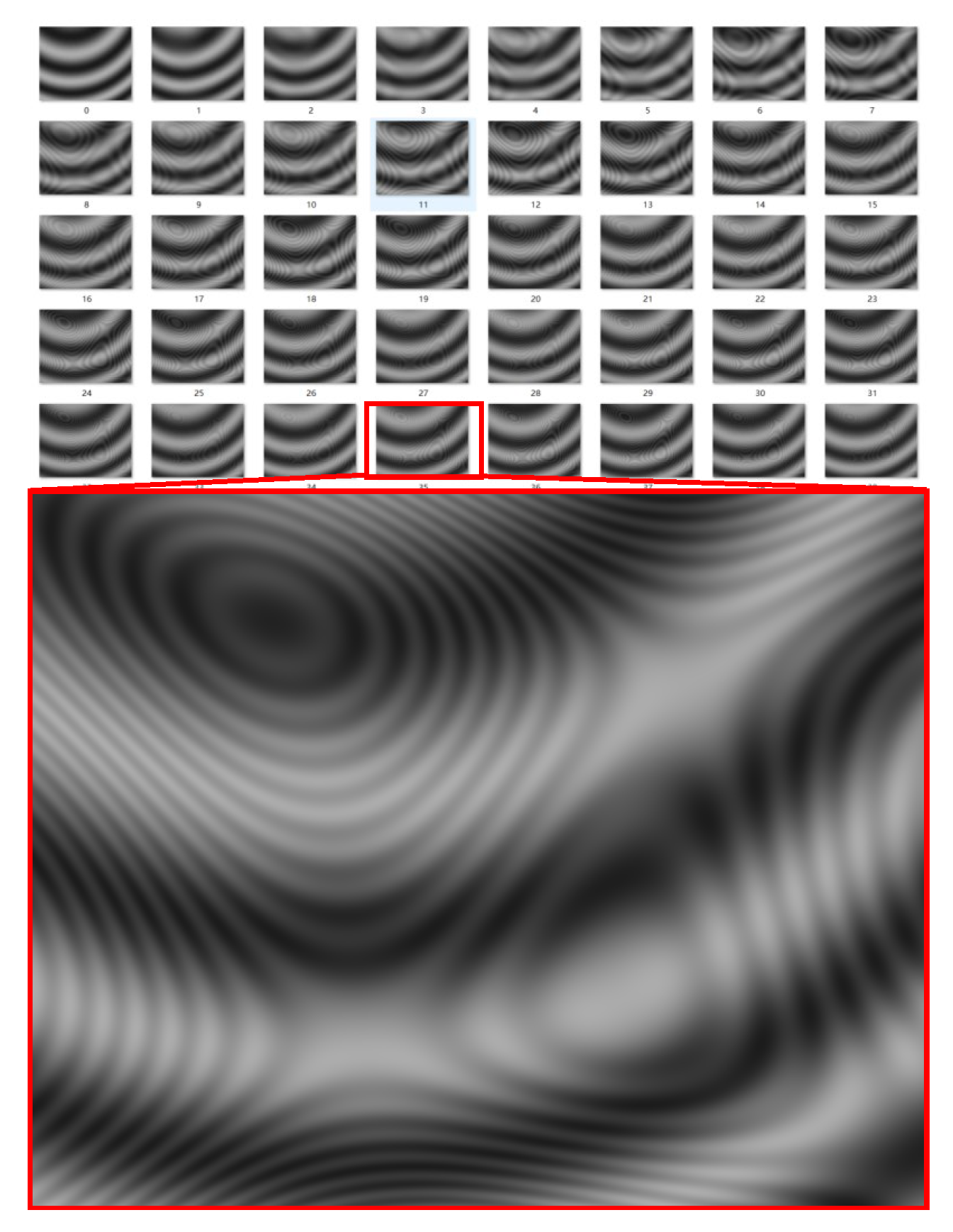
In order to preliminarily verify the influence of multi-facial interference on the structural characteristics of the signal, and to provide an intuitive basis for the design of the subsequent phase resolution method, this paper carries out a numerical simulation and frequency domain analysis study for the interference signal of the three-layer reflection surface. By constructing an idealized three-interface reflection model and simulating the interference signal under typical incidence conditions, it can be observed that the interferogram shows an obvious periodic stripe superposition effect. In
Figure 3, a fast Fourier transform (FFT) analysis reveals that the signal exhibits multiple characteristic peaks in the frequency spectrum, which correspond to the FM interference components induced by different optical range differences [
28]. During the simulation, the reflectivity of the simulated rear surface is relatively high, resulting in a relatively large amplitude of the interference signal on the rear surface. These frequency domain features form a consistent correspondence with the spatial shape of the interference fringes in the simulation plots. From the perspective of frequency characteristics and phase evolution, the optical range difference and refractive index difference of different reflecting surfaces jointly act on the oscillation period and envelope modulation of the interfering fringes, resulting in the composite signals showing a recognizable multilayer interferometric structure in both the spatial and frequency domains [
29]. Although this simulation results is an ideal model, it effectively reveals the non-simple harmonic interference behavior brought about by the multiple reflection interfaces, which provides an analytical basis for the robustness verification of the subsequent algorithms in the context of complex signals and parameter selection.
3. Reconstruction Algorithm
In wavelength-tuned interferometry oriented to the dual-surface topography solution for the Si/SiC semiconductor thin films, the traditional least-squares iterative method faces the following three core challenges: the overlapping of more than third-order harmonics generated by multi-surface reflections from the thin films, such as the frequency-domain overlapping of the upper and lower surfaces–reference mirror interference fundamental, the second harmonic of lower and upper surface interference, and the third harmonic of the substrate spurious reflections [
30]; the reflectance due to the difference in process asymmetry, typical SiC thin film upper surface reflectivity, the lower surface, so that the interference signal intensity ratio increases, triggering the Jacobi matrix pathology problem; in addition, the refractive index spatial modulation induced by the doping concentration gradient [
31], resulting in the effect of a nonlinear phase term. To address the need for the high-precision solving of dual-surface morphology of the Si/SiC semiconductor thin films, this paper proposes a high-precision surface reconstruction algorithm for suppressing multiple harmonics of the SiC/Si thin films, whose core innovation lies in the integration of harmonic spectral-domain decomposition, physical constraints on the refractive-index gradients, and over-sampling–partitioning optimization, which systematically improves the solving accuracy of the traditional methods in harmonic aliasing, matrix pathology, and nonlinear phase modulation. On the basis of Equation (1), the influence of multiple harmonics is introduced, and the following expression for the interferometric light intensity in the actual measurement state is obtained:
where
is the DC component of the interference signal,
is the mth order harmonic component,
is the target phase to be solved,
is the initial phase fixed for the system, and
includes the nonlinear phase error introduced by the doping gradient and other non-ideal factors. In conventional least squares optimization, the objective is to solve the parameter vector by minimizing the sum of squares of the residuals between the measured light intensity and the model predictions, as follows:
Define the weightless objective function as follows:
In the Gauss–Newton method, assuming that the estimated parameter
is available at the first iteration, a first-order Taylor expansion of the model yields the normal equations in the algorithm. The Gauss–Newton method can quickly capture local features of the semiconductor wafer surface, such as small deformations and fluctuations, by iteratively optimizing the solution results, thus providing a basis for global optimization.
where the Jacobi matrix
is as follows:
Let the residual vector be the following:
Then the standard Gauss–Newton update formula is as follows:
In multi-harmonic interference, the higher-order harmonics (especially in low SNR scenarios) are often severely affected by aliasing and noise, and if the traditional least-squares method is directly adopted, the parameter update will be over-sensitive to these weak signal components [
32], which leads to an elevated Jacobi matrix condition number and triggers iterative instability. For this reason, we introduce a dynamic weighting strategy that assigns different weights to each harmonic component in the residual term and the Jacobi matrix, respectively. This is accomplished by weighting the error between the residual and the model value of each harmonic component, and then accumulating these weighted errors to form a new objective function [
24]:
where
and
denote the measured and model-predicted values of the mth order harmonics, respectively. The weights
are dynamically adjusted according to the signal-to-noise ratio, amplitude magnitude, and reflectivity asymmetry of each order harmonic in the current iteration. Specifically, lower order harmonics are usually assigned higher weights, while lower weights are applied to higher order harmonics to minimize interference [
33]. During the initial phase of the iterative algorithm, initial weights are assigned to the harmonic components based on a stepwise optimization strategy that accommodates varying material and thickness conditions. By calculating the signal-to-noise ratio (SNR) and amplitude ratio, we evaluate the measurement quality of each harmonic component and set the initial weights accordingly. The SNR reflects the strength of the signal relative to the noise, while the amplitude ratio indicates the proportion of the actual measured amplitude to the theoretical maximum amplitude. The initial weights are determined by the product of the SNR and the amplitude ratio, and are normalized by a factor α to ensure a total sum of 1. The SNR quantifies the signal strength relative to the background noise, while the amplitude ratio assesses the measured amplitude against the theoretical maximum. An assessment of these parameters allows for dynamic weight adjustment during the iterative process, prioritizing data with a high SNR, thereby enhancing measurement accuracy. This approach ensures the algorithm’s adaptability to different measurement conditions and optimizes weight distribution for more precise surface measurements of semiconductor wafers [
28]. After introducing the weights, the residual function becomes the following equation:
Accordingly, the partial derivatives of the parameters are multiplied by the corresponding weights. Let the original Jacobi matrix be as follows:
Construct a diagonal weight matrix as follows:
In this way, the corrected Jacobi matrix is as follows:
From this, a weighted residual and modified Jacobi matrix is used, where the residual vector is weighted as follows:
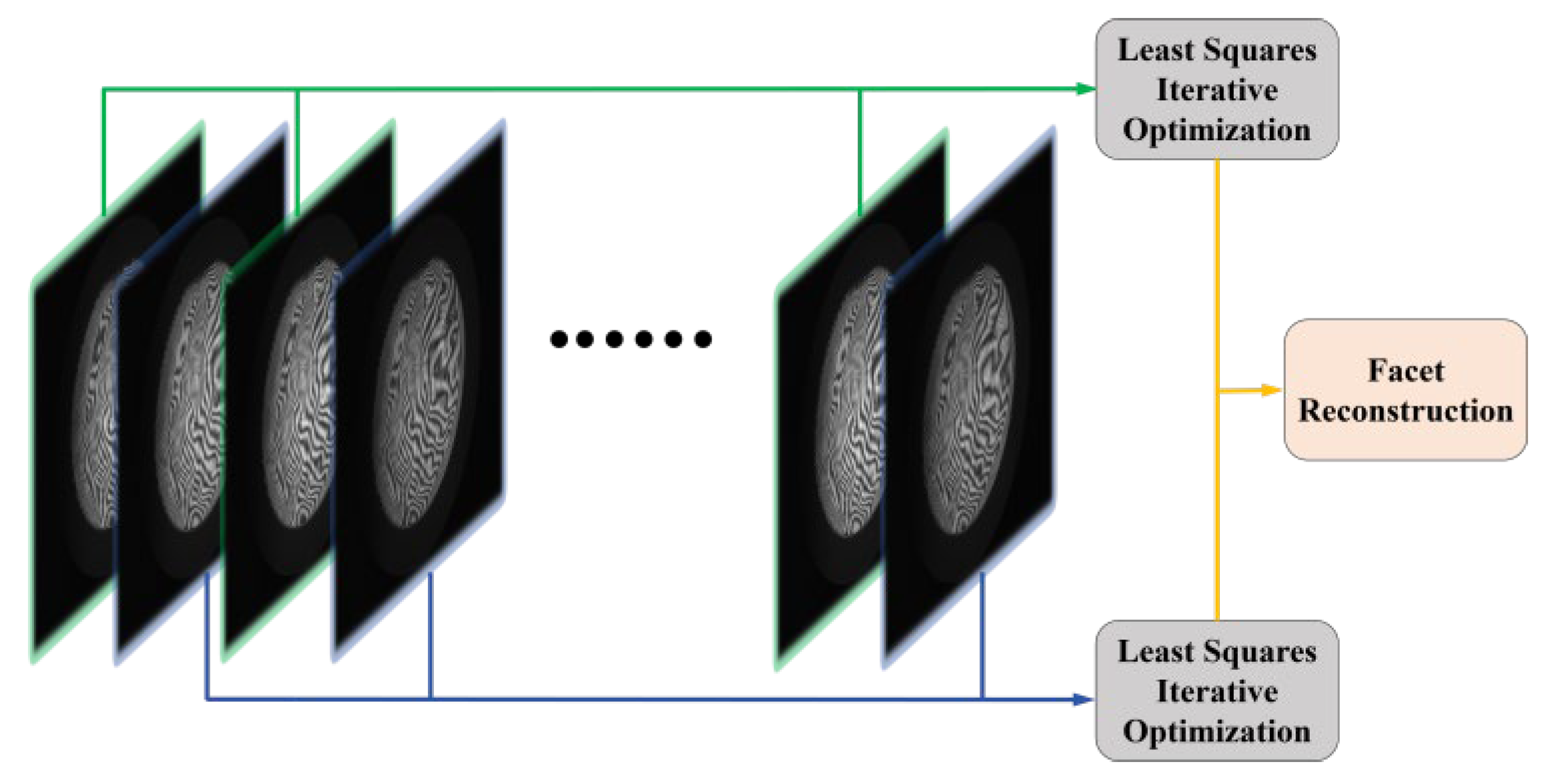
The original sampling step size is changed to half of the original, after which continuous acquisition is carried out, and the collected interferometric image data are divided into two groups,
and
, at equal intervals;
and
are solved in each group and, due to the relatively small amount of data and the short time interval between the acquisition times, the effects of the systematic error and transient vibration can be locally controlled so as to obtain a stable preliminary phase estimation. After obtaining the phase solution results of groups
and
, respectively, the statistical advantage brought by data redundancy is utilized, and the fusion strategy is adopted to further improve the overall phase solution accuracy [
34]. According to the residuals or the goodness-of-fit of the solution results for each group, assign the corresponding weights,
,
, to each group, and calculate the weighted average phase as follows:
In
Figure 4, the setting of the weights can be dynamically adjusted based on the signal-to-noise ratio of each group, fitting residuals and other indicators. Analyzing the phase distribution of each group can optimize the detection of outliers that may occur due to sudden vibration or high harmonic interference [
34]. The robustness of the final solution is improved by eliminating the outlier groups or correcting the outliers, and then re-entering the local least squares iteration [
33,
35] using the fused result as the new initial value. When there are local anomalies in a single set of data due to systematic errors, transient vibrations, or multiple harmonics, other sets of data usually provide more accurate information. Fusing multiple sets of results significantly reduces the impact of a single set of anomalies on the overall phase solution. Statistical averaging of multiple sets of phases can effectively reduce the standard deviation of random noise, thus improving the accuracy of the measurement. The fusion strategy makes the overall method more resistant to various types of random disturbances and systematic errors, and is suitable for the compensation of multiple undesirable factors in complex interferometric systems.
4. Experimental Results and Discussion
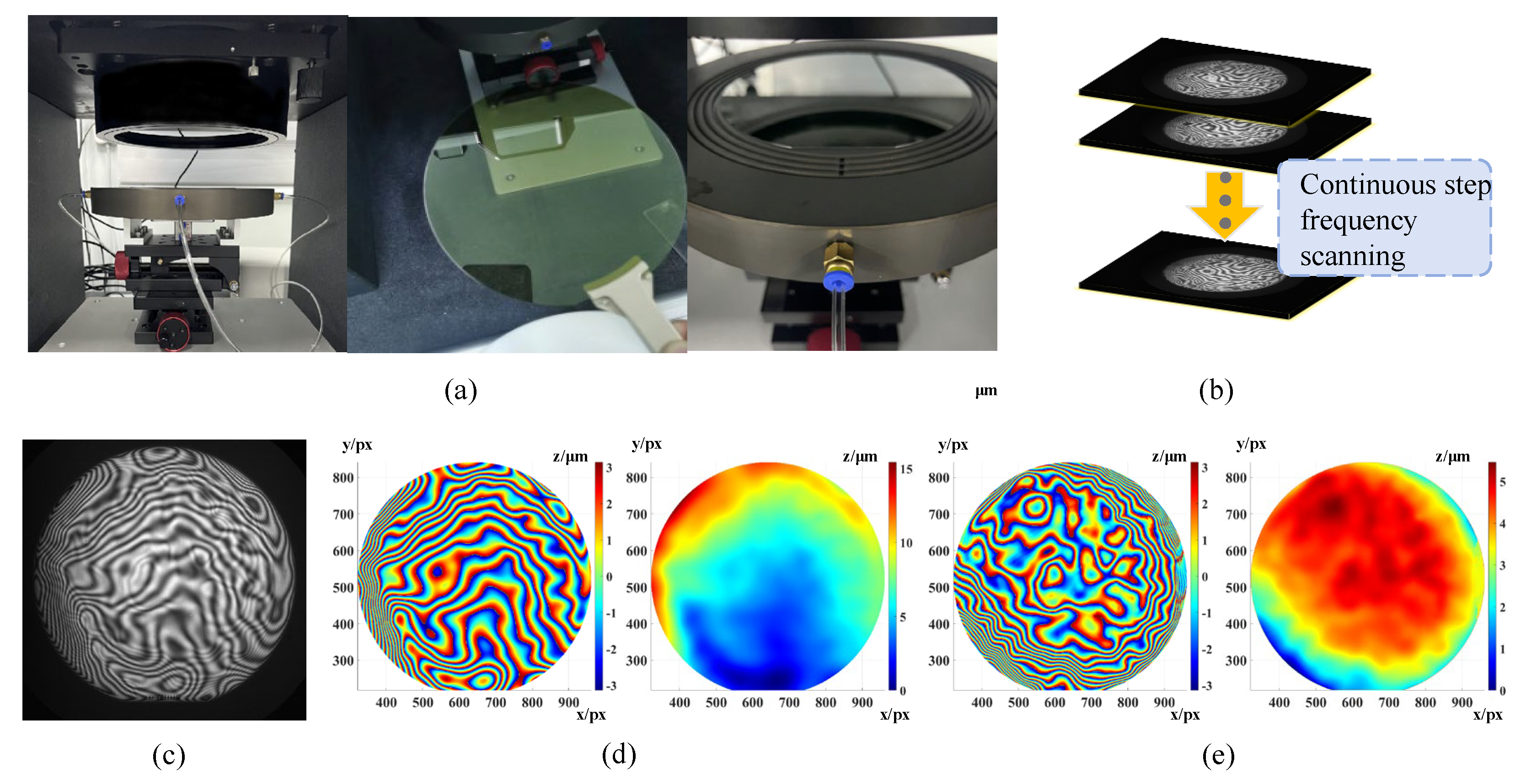
In order to verify the effectiveness of the proposed method in SiC/Si multilayer surface interferometry, a high-precision optical measurement system is constructed in this paper. The optical part adopts the Fizeau interferometric optical path, and the interferometric image of the wafer surface is obtained by a near-infrared high-resolution camera; the high sensitivity and low-noise performance of the camera effectively ensure the accuracy and reliability of the data and, at the same time, the stability and consistency of the interferometric system are monitored in real time by using the optical path alignment camera [
36]. The mechanical part of the ultra-fine hole vacuum adsorption of alumina suction cups, processing flatness better than 3 μm, can be firmly fixed 6-inch wafers and provide uniform suction. Suction cups position the adjustment table to achieve the wafer incidence angle and the precise adjustment of the optical path. The overall rigidity of the marble base support platform can significantly reduce the interference of environmental vibration on the measurement accuracy. Through the comprehensive design and construction of the above optical system, this paper builds a multi-surface interferometry platform that can meet the high-precision requirements of semiconductor thin-film surface measurement.
In the semiconductor industry, the flatness tolerance of silicon wafers varies with process requirements and product types. According to SEMI standards, the warpage of 8-inch silicon wafers should generally be less than 20 μm, and the maximum allowable warpage of 6-inch silicon wafers is also 10 μm [
7]. However, through communication with the wafer fab process personnel and actual on-site testing, we found that double-polished silicon wafers generally have higher flatness, and the tolerance is generally within ±1 μm. Due to the surface stress effect of oxide-coated silicon wafers, local stress deformation may occur, resulting in flatness deviations of up to ±5 μm. Due to the brittleness of silicon carbide wafers and the influence of the manufacturing process, the flatness deviation may even reach ±10 μm or even higher. (Note: The horizontal and vertical coordinate units of all silicon wafer three-dimensional pseudo-color images in the article are in pixels (px). The resolution calculation formula includes actual size (mm) divided by the number of pixels (px), which is 0.22.)
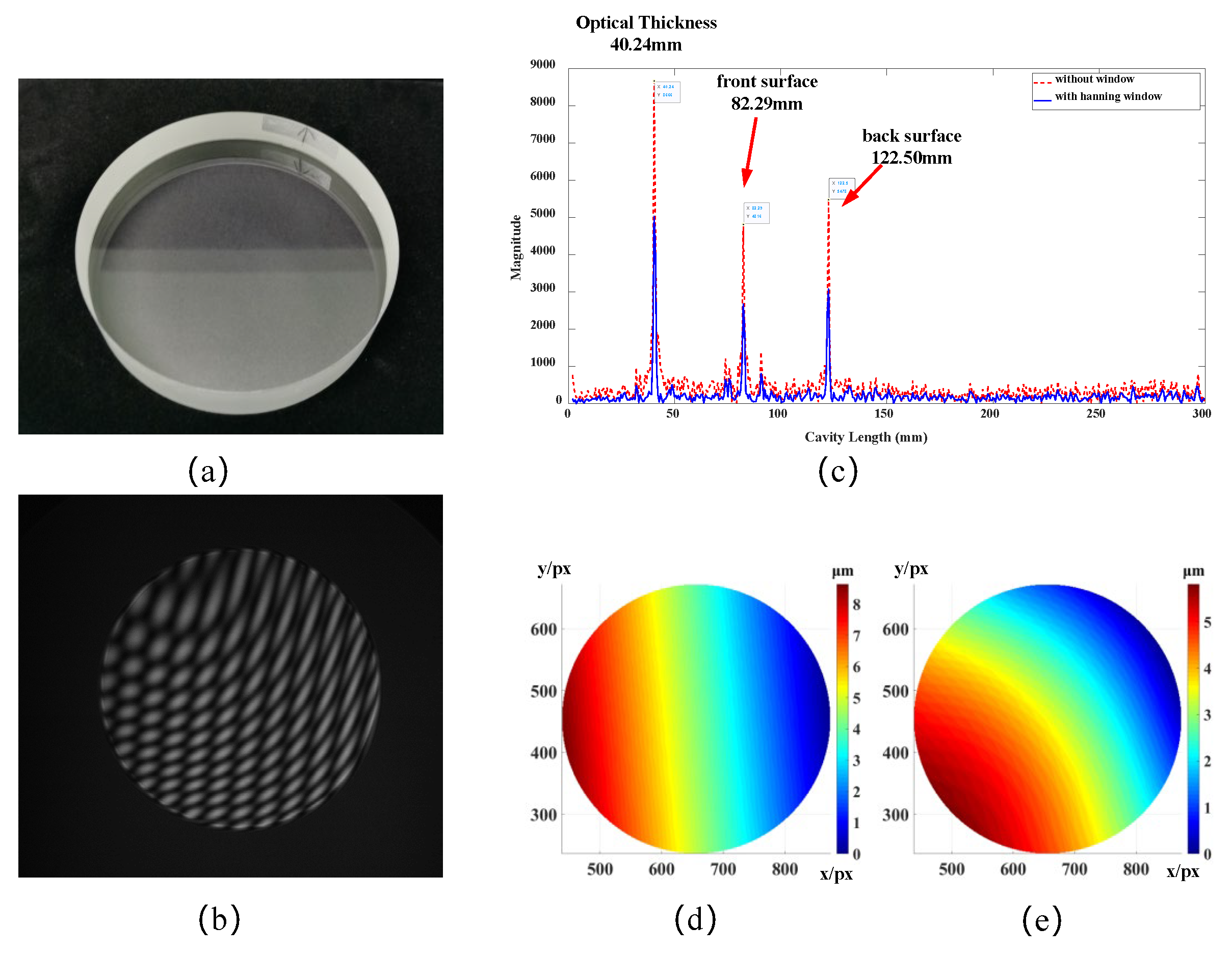
In
Figure 5, during the measurement process, the composition of the optical path and the measured light flow are as follows: The beam generated by the laser is transmitted via a fiber optic coupler to the interferometer, where a diffusion element extends the beam to optimize coherence and illumination uniformity. A beam splitter shapes and projects the beam to the reference mirror of the Fizeau interferometer, where part of the beam is reflected as reference light, and the rest of the transmitted light illuminates the wafer as test light. The test light reflected from the wafer and the reference light generate interference fringes at the beam splitter, and the interference fringes are continuously captured by a high-resolution camera and transmitted to a computer. The three-dimensional shape of the wafer is reconstructed by algorithmically separating the signals on each surface. The key parameters, such as total thickness variation (TTV), thickness (Thk), bowing of the upper surface (Bow), and warpage (Warp) of the output wafer, are in accordance with the SEMI standard of the semiconductor industry [
7]. In
Figure 6, experimental tests were conducted on silicon wafers with different materials and wavelength transmittance, covering SiC (substrate wafers), SiC (epitaxial wafers), Si (double-polished wafers), Si (coated wafers), and K9 optical glass. The system is capable of measuring silicon wafers with diameters ranging from 4 inches to 8 inches, and ensures that the measurement time is kept to less than 1 min during the individual wafer acquisition and resolution process.
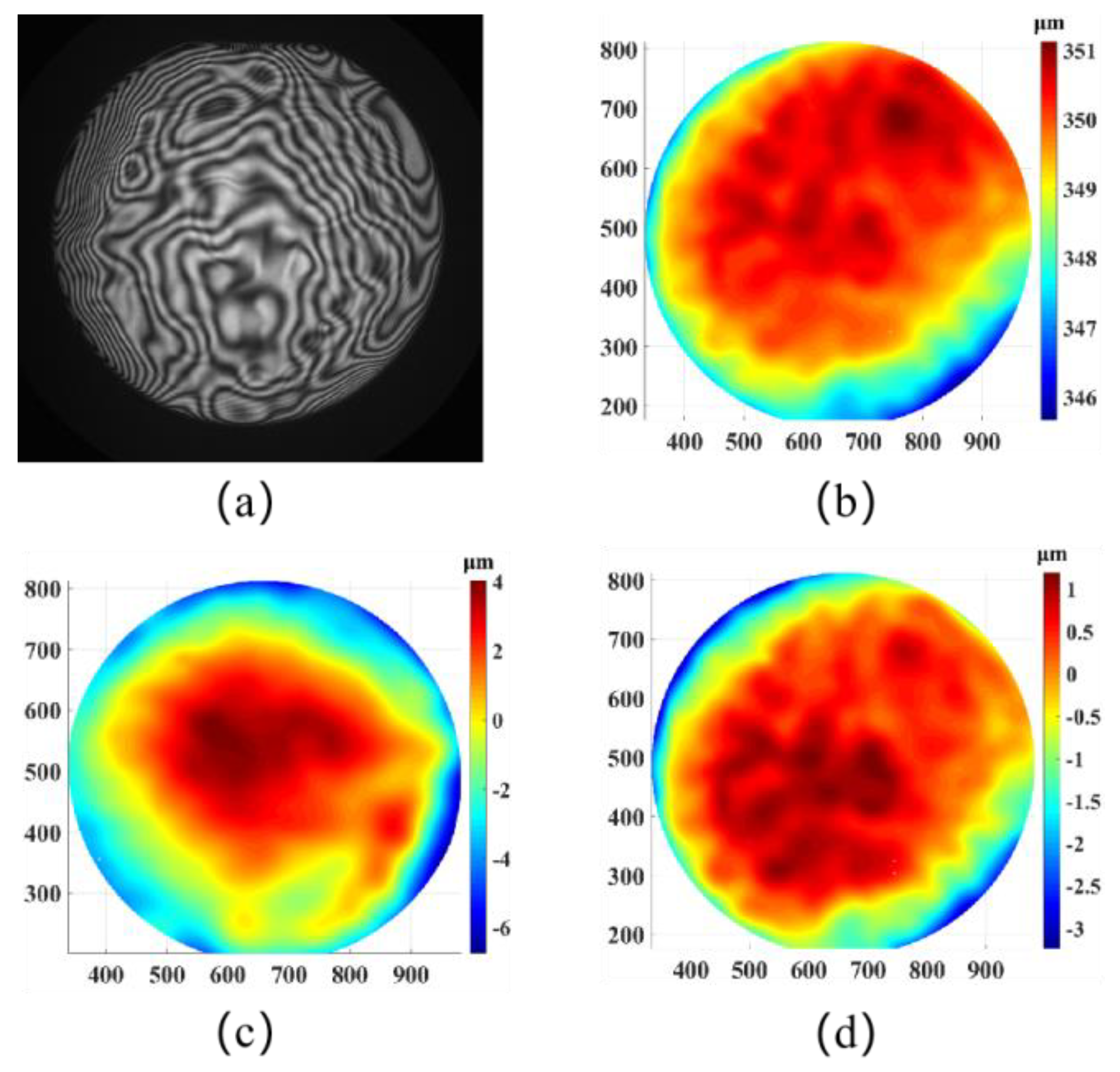
In
Table 2, the experimental results show that the SiC samples exhibit good surface flatness and stability of deformation characteristics in multiple measurements.
Figure 7 visualizes the surface topography and deformation of the samples through interferograms, back-reference plots, bow-deformation plots, and median surface plots. In
Table 3, the repeatability of the frequency scanning interferometry system was evaluated, and the results showed that the repeatability standard deviation (RSD) of the system was 2.0%, 0.4%, and 0.5% for the measurement of the thickness variation volume (TTV), warping (Warp), and bowing (Bow), respectively. The repeatability measurement data in
Table 2 show that the TTV, Warp, and Bow deformations have less fluctuation in multiple measurements and have good repeatability and consistency. Specifically, in
Table 2 the PV values of the TTV, warpage, and bow deformation were 0.352 μm, 0.195 μm, and 0.107 μm, respectively, which further verified the stability of the measurement results. The system not only solves the face shape of the upper and lower surfaces, but completes the full-size reconstruction of the surface topography of multilayers, and outputs 15 flatness parameters, including thickness (Thk), thickness variation (TTV), bowing (Bow), and warping (Warp) of the upper surface.
During the experiments, during the measurement of the SiC and Si wafer, due to the process limitation, the upper surface has higher signal strength and is easy to measure, while the lower surface has weaker signals due to the flake process or the backside roughness problem, resulting in insufficient interferometric signals, which makes it difficult to measure the upper and lower surfaces accurately at the same time with the near-infrared transmission method. To overcome this limitation, we propose an innovative measurement method, as shown in
Figure 8. First, the face shape and absolute distance of the suction cup surface were accurately determined before measurement. Then, the face shape of the upper surface of the sheet was measured in the suction cup adsorption state, and then the suction cup adsorption was turned off so that the sheet was in a free state, and the upper surface face shape was measured again. Through data processing and comparative analysis, the face shape and total thickness variation (TTV) of the upper and lower surfaces can be accurately calculated.
This method not only effectively solves the limitations when transmittance measurement is not possible, but significantly improves the adaptability and accuracy of the measurement of the SiC and Si thin films. With this method, the surface properties of the thin films can be evaluated more comprehensively, increasing the compatibility and versatility of this measurement method.
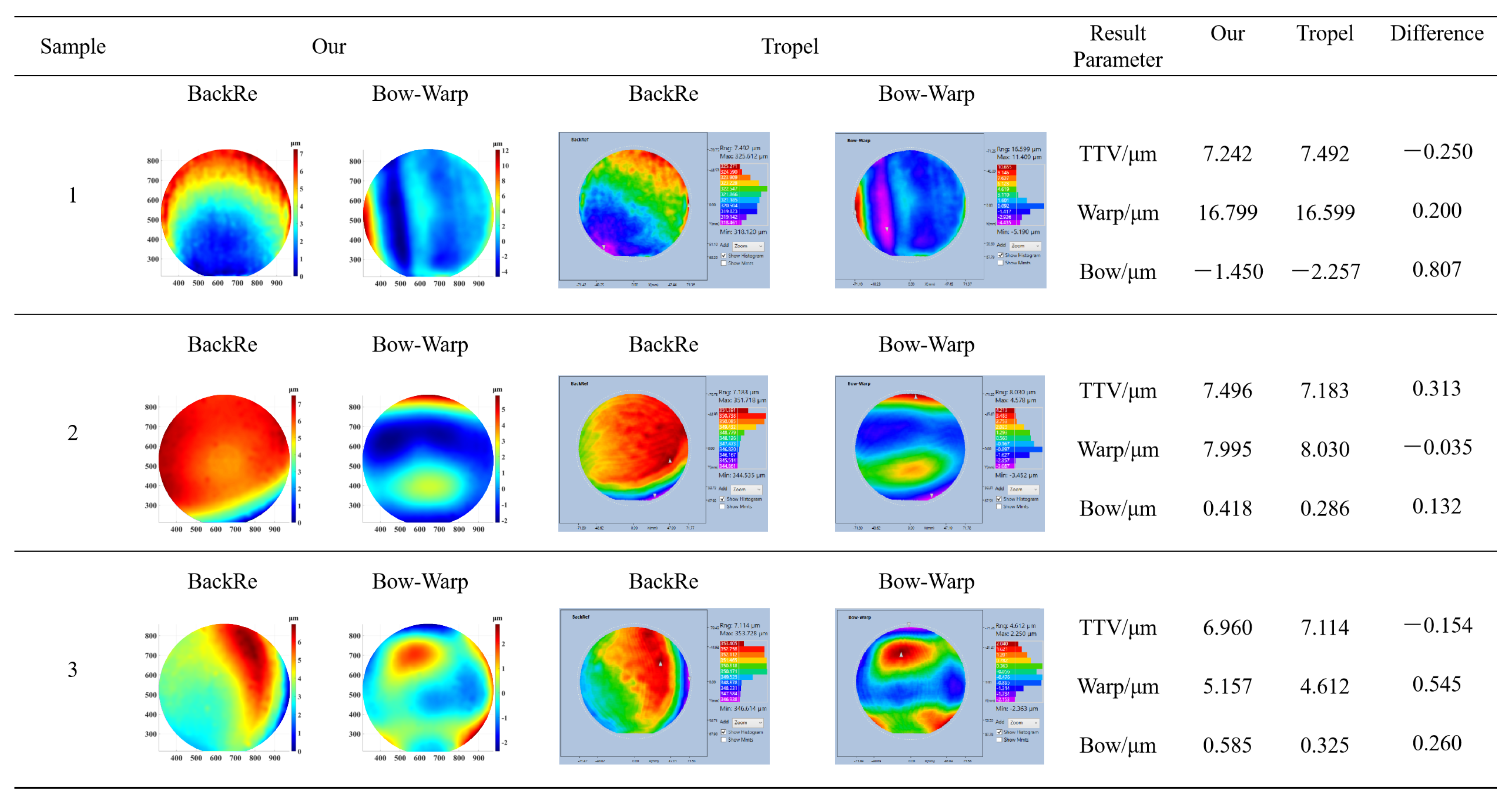
This study compares the performance of the current measurement system with a commercial Corning Tropel instrument in a variety of optical surface measurements. The results are shown in
Figure 9. It can be inferred that the comparison shows a high degree of agreement in terms of measurement accuracy and stability, with data distribution and error ranges showing general agreement. Specifically, the current system provides comparable results to the Corning Tropel when measuring different SiC wafers. In high-precision measurements, the data distributions and error distributions of the two measurements are highly consistent, verifying the reliability and accuracy of the current system. Analyzed from both qualitative and quantitative perspectives, the measurement results of the current system are highly consistent with those of the Corning Tropel, further confirming the accuracy and consistency of its measurement results. Meanwhile, the near-infrared light source used in this study, which can penetrate the Si-based semiconductor sheet, is the biggest advantage over the visible light source of Corning Tropel. In addition, we introduced the suction cup measurement method to improve the applicability and versatility of the measurement of thin films with different processes, which effectively compensates for the impact of the restricted measurement of process differences and ensures the accuracy and consistency of the measurement. In summary, the current measurement system is comparable to Corning Tropel in terms of measurement accuracy, stability, and complex surface processing capability, and has better applicability to semiconductor thin wafers.
5. Conclusions
In this paper, a set of a high-precision frequency scanning interferometric solving algorithm and a frequency scanning interferometry system are proposed and realized for the core problems of harmonic aliasing, refractive index asymmetry, and nonlinear phase modulation faced by the Si/SiC multilayer thin film in thickness, flatness, and double-surface topography measurement. A high-precision surface reconstruction algorithm is proposed to suppress the multiple harmonics of the SiC/Si thin film, and the high-order harmonic interference caused by multiple reflections is significantly suppressed by harmonic spectral domain decomposition, refractive index gradient constraints, and partitioning optimization strategy; and the means of “over-sampling” and weighted fusion of multiple sets of data are utilized to effectively enhance the multi-harmonics of semiconductor thin film. The robustness and accuracy of the semiconductor wafer multi-surface reconstruction solution under random vibration and systematic errors are effectively improved by the means of “oversampling” and weighted fusion of multiple data sets. The experimental results show that, in the measurement of the 6-inch Si/SiC wafers, the system is able to synchronously obtain the three-dimensional morphology of the upper and lower surfaces, and reconstruct the key parameters, such as flatness, warpage, and thickness variation (TTV), and the comparison with the Corning Tropel FlatMaster commercial instrument shows a high degree of consistency and excellent applicability. In order to extend the versatility of the measurement system, the use of a near-infrared light source that can penetrate the Si substrate, combined with the suction cup measurement method, overcomes the limitations of the traditional visible light interference in the backside detection and measurement of materials with high refractive indices, and provides the possibility of subsequent on-line measurements in complex scenarios, such as SiC substrates, high-power devices, and epitaxial layer structures. The opto-mechanical system and algorithm framework constructed by this research institute not only realizes the accurate measurement of multilayer surface topography of third-generation semiconductor wafers, but lays a solid foundation for the subsequent expansion to more kinds of composite wafers, and improves the measurement speed and anti-interference ability. In the future, more physical models and online calibration strategies will be integrated to further enhance the real-time inspection performance of the system in harsh manufacturing environments, such as high temperature and high frequency, to provide a more reliable means of measurement and quality control for the preparation of new-generation power and RF devices.

 ,
, 


