Abstract
Thin-film lithium niobate (TFLN) electro-optic modulators serve as critical components in microwave photonic systems. To improve device performance, we developed a U-T double-layer traveling-wave electrode configuration. Using finite element analysis, we systematically simulated and optimized both modulation efficiency and radiofrequency characteristics, ultimately realizing a low half-wave voltage-length product of 1.77 V·cm, a minimal optical loss of 0.022 dB/cm, and an ultra-wide modulation bandwidth surpassing 100 GHz.
1. Introduction
Functioning as the central device in microwave photonic systems, electro-optic modulators enable high-fidelity electrical-to-optical signal conversion while accurately controlling critical optical parameters including wave frequency and phase. The modulator plays a governing role in determining data transmission rates within optical communication systems, serving as an essential element in addressing contemporary demands for ultra-high-speed data transfer. The refinement of its operational characteristics proves vital for system-level performance enhancement, ultimately necessitating adherence to rigorous performance metrics and operational benchmarks.
Electro-optic modulator fabrication predominantly utilizes semiconductor materials including silicon (Si), indium phosphide (InP), and lithium niobate (LiNbO3). While Si-based and InP modulators exhibit specialized performance merits in niche applications [1,2,3], substantial constraints persist when addressing the core specifications of contemporary telecommunication systems, particularly regarding the realization of ultra-wide modulation bandwidth exceeding 60 GHz, the suppression of half-wave voltage (), the and mitigation of propagation losses. By comparison, LiNbO3 leverages exceptional electro-optic characteristics encompassing pronounced Pockels coefficients, extended spectral operability, and well-established manufacturing protocols [4,5], rendering LiNbO3-based modulators decisively superior to conventional material implementations in terms of integrated device performance.
In contrast to conventional bulk LiNbO3, thin-film LiNbO3 (TFLN) preserves intrinsic material merits, including ultra-low propagation loss and pronounced linear electro-optic response [6,7], while achieving enhanced modulation efficiency through a substantial reduction in electrode–waveguide gap dimensions, and this advancement further enhances device compactness, facilitating the further miniaturization of the device. Importantly, this merit enables the lithium niobate (LN) platform to incorporate high-performance components such as ultra-high-Q micro-resonators, programmable filters, and low-loss delay lines [8]. These components could potentially integrate with highly linear electro-optic modulators monolithically on the same photonic chip, thereby realizing more sophisticated microwave photonic functionalities. Thin-film LiNbO3-based modulators exhibit benchmark performance characteristics: ultra-wide operational bandwidth, a superior extinction ratio (>30 dB), negligible chirp distortion, and exceptional long-term reliability. Owing to these salient performance merits, TFLN has emerged as the material of choice in advanced electro-optic device fabrication, providing a solid technical foundation for next-generation high-speed communication systems.
In 2018, Harvard University’s Marko Loncar group pioneered revolutionary advancements in lithium niobate-on-insulator (LNOI) photonic integration [9]. Employing X-cut LiNbO3 wafers with advanced nanofabrication techniques, they demonstrated the first CMOS-foundry-compatible electro-optic modulator platform. This breakthrough fundamentally resolved the critical limitations of bulk devices including excessive footprint, prohibitive cost, narrow bandwidth, and high , establishing LNOI as a paradigm-shifting platform that provided foundational theoretical frameworks for next-generation photonic integration. In 2021, Tsinghua University’s Yi Luo group introduced an innovative CL-TWE (capacitively loaded traveling-wave electrode) architecture [10]. This structure achieved phase velocity matching between microwaves and optical waves through the introduction of quartz substrate, while significantly reducing microwave transmission losses, thereby greatly enhancing the device’s operational bandwidth. In 2022, Zhejiang University’s Liu Liu team refined the CL-TWE design [11] through substrate removal techniques on silicon platforms, realizing microwave deceleration with improved velocity matching and reduced propagation losses via localized substrate etching, ultimately achieving superior bandwidth characteristics.
These advancements have unequivocally validated the remarkable performance superiority of thin-film LiNbO3-based electro-optic modulators. Future investigations will focus on three critical dimensions: continued reduction in driving voltage requirements, the systematic expansion of operational bandwidth, and the refined optimization of velocity matching characteristics—representing both focal points and persistent technical challenges.
2. Fundamental Operating Principles of Electro-Optic Modulators
The proposed TFLN electro-optic modulator architecture comprises two integrated functional domains: an optical manipulation unit and an electrical driving unit. The optical manipulation unit employs a Mach–Zehnder Interferometer (MZI) structure, which forms a complete interference optical path through two multimode interference (MMI) beam splitters and centrally symmetric distributed TFLN ridge waveguides.
This TFLN electro-optic modulator achieves optical signal modulation based on the linear electro-optic effect (Pockels effect) of lithium niobate crystals. The underlying physical principle manifests as a deterministic linear relationship between the extraordinary refractive index and the transverse electric field. The specific modulation process is as follows: first, the input optical signal is equally divided into two symmetrically distributed TFLN ridge waveguides through an MMI splitter; then, by applying external electric fields with opposite phases to the parallel modulation arms, a controllable phase difference is generated; and finally, after combining through the interferometer, the phase modulation is converted into the intensity modulation output.
The modulated optical intensity is governed by the transfer function:
The phase shift induced by an applied electric field during optical wave propagation through a waveguide of length L can be expressed as follows [12]:
where denotes the optical wavelength in vacuum and indicates the refractive index variation in x-cut TFLN, with its mathematical formulation expressed as follows:
where represents the extraordinary refractive index in the Z-crystallographic direction of the LiNbO3 substrate. corresponds to the principal electro-optic coefficient tensor component () in lithium niobate, V denotes the externally applied bias voltage, g represents the electrode spacing, and Γ corresponds to the electro-optic confinement factor, mathematically expressed by the following [13]:
where corresponds to the microwave electric field spatial profile and E0 characterizes the optical mode intensity distribution in the waveguide.
In the unbiased operational state of the TFLN modulator, a zero-phase differential () is maintained between the dual MZI arms, resulting in complete optical field reconstruction at the output port. Upon the application of an external electric field inducing a π-phase shift () in the waveguide arms, the output optical intensity demonstrates destructive interference, as analytically predicted by Equation (1). The voltage required to induce π-phase modulation in the optical waveguide arm is formally defined as the half-wave voltage (); through the systematic derivation of Equations (2)–(4), the analytical expression is obtained as follows:
Therefore, constitutes a pivotal performance metric in electro-optic modulators, serving as a direct indicator of the device’s modulation sensitivity. A reduced value correlates with enhanced electric field responsivity in the modulator, enabling equivalent phase modulation with lower driving voltage amplitudes, thereby achieving reduced operational power consumption while enhancing modulation efficiency in photonic integrated systems.
3. Microwave–Photonic Electrode Structure Design
Figure 1 presents the optimized device architecture of the proposed X-cut TFLN Mach–Zehnder modulator (MZM). Figure 1a depicts the cross-sectional epitaxial configuration of the active modulation region, while Figure 1b illustrates the microwave optical velocity-matched copropagating electrode design. The multilayer heterostructure consists of (from bottom to top) the following: a 500 μm-thick silicon substrate, 4.7 μm thermally grown SiO2; buffer layer, 0.6 μm single-crystal X-cut LiNbO3; film incorporating 1.5 μm-wide ridge waveguides, and an 800 nm-thick SiO2 upper cladding layer. By leveraging the inherent push–pull electro-optic mechanism characteristic of X-cut LiNbO3 platforms, where the refractive index modulation depends on the crystal orientation governed by the third-rank electro-optic tensor (), the implemented ground–signal–ground (GSG) electrode configuration generates complementary phase shifts () in the dual interferometric arms through domain inversion engineering [14]. This design strategy effectively enhances the half-wave voltage-length product () performance. Table 1 lists the specific parameters of the structure, while subsequent chapters will detail the design and simulation processes.
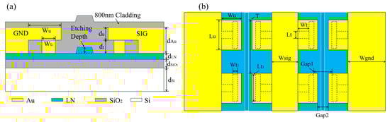
Figure 1.
(a) Schematic diagram of the modulation region cross-section; (b) schematic of the traveling-wave electrode structure.

Table 1.
The detailed parameters of the individual structures designed in this work.
3.1. Simulation Analysis of Modulation Region
Electromagnetic simulations were conducted to investigate transverse electric (TE) mode field characteristics. Parametric models incorporating varied etching depths and electrode gap dimensions were systematically simulated. The resulting field distribution, optical propagation loss, and are presented in Figure 2 and Figure 3. Field distribution analysis revealed geometrically dependent relationships between waveguide dimensions and optical confinement characteristics: an increase in etching depth and electrode gap width reduces the optical attenuation induced by electrode absorption, while concurrently elevating the . This fundamental compromise stems from competing physical phenomena—wider electrode gaps diminish lateral electric field intensity, whereas deeper etching enhances optical mode confinement, thereby reducing the spatial overlap between optical and microwave fields. The inverse correlation between electric field magnitude and optical confinement efficiency establishes an inherent performance balance between reduced and minimized optical propagation loss. Consequently, device optimization necessitates careful consideration of both reduction and optical loss suppression. Through systematic dimensional parameter optimization, enhanced modulator performance can be achieved.
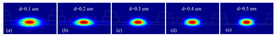
Figure 2.
(a–e) Electric field intensity distribution variations at different etching depths.
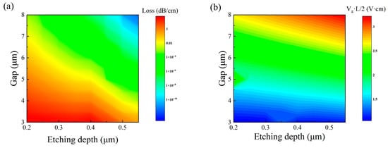
Figure 3.
Contour plots of (a) waveguide loss and (b) half-wave voltage product under different electrode spacings and etching depths.
A 0.3 μm etching depth configuration was implemented to investigate the dependence of optical propagation loss and on the electrode spacing parameters gap1 (T-structure) and gap2 (U-structure), as illustrated in Figure 4. The experimental findings demonstrate a consistent reduction in optical loss accompanied by the progressive elevation of with increasing gap1 dimensions, whereas gap2 adjustments manifested negligible impacts on both photonic characteristics. The parametric analysis enabled the optimization of gap1 to 5 μm, while gap2 dimensions were fundamentally governed by the geometric constraints of the U-shaped coplanar waveguide electrode geometry.
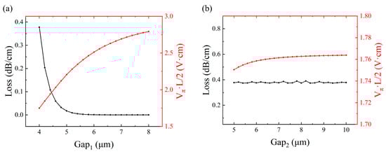
Figure 4.
Optical loss and half-wave voltage product under varying (a) gap1 and (b) gap2.
Subsequently, we conducted simulations on the thickness of the dual-layer electrodes. Given that the total thickness of the T and U electrode layers matches the main electrode thickness, we exclusively present the simulation results for the lower T-layer thickness, as shown in Figure 5. It is evident that with the variations in T-layer thickness, the demonstrates a nearly linear variation pattern, whereas the optical loss displays an exponential variation characteristic. Through comprehensive consideration, dt = 0.6 μm was determined as the optimal configuration.
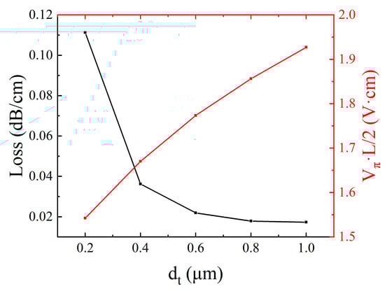
Figure 5.
Optical loss and half-wave voltage product under varying dt.
This optimized configuration achieves an effective compromise between optical attenuation and electro-optic driving voltage, thereby ensuring enhanced modulation efficiency in the implemented device.
A systematic investigation was conducted on the radiofrequency (RF) characteristics of the electro-optic modulator. Conductor-induced attenuation was identified as the primary contributor to microwave transmission performance deterioration. The electromagnetic dissipation mechanism was decomposed into two distinct components: The first mechanism involves Ohmic loss generation through intrinsic material resistivity during current propagation in conductive paths. The second component arises from current distribution confinement near conductor surfaces induced by the skin effect. Inadequate metal electrode thickness results in pronounced surface current density intensification, producing supplementary electromagnetic losses. To quantitatively evaluate electrode thickness dependencies, parametric electromagnetic field simulations were executed across varying metallization thickness configurations. The simulation results detailing these thickness-dependent characteristics are comprehensively presented in Figure 6.
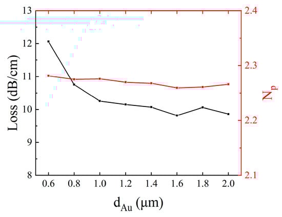
Figure 6.
Variations in RF loss and refractive index with varying metal electrode thickness.
Numerical simulations demonstrate the stabilization of RF losses beyond a 1 μm electrode thickness. This phenomenon stems from current crowding suppression when metallization thickness surpasses the skin depth threshold, thereby reducing resistance-induced dissipation through the mitigation of current over-concentration. Crucially, the effective microwave refractive index (Np) exhibits thickness-independent behavior with insignificant parametric variation. Electrode thickness optimization therefore principally addresses microwave attenuation constraints, though requires the integrated consideration of fabrication economics and potential electric field distortion from excessive metallization. Comprehensive multi-criteria analysis identifies 1.2 μm as the optimal thickness configuration. This parameter selection maintains subcritical RF losses while achieving performance–cost equilibrium, effectively suppressing conductor-induced power dissipation without introducing the fabrication complexities or field uniformity degradation associated with over-thickened electrodes.
The investigation was extended to microwave propagation modulation characteristics in U-shaped electrode architectures. Computational electromagnetic analysis was employed to resolve the parametric dependencies of electrode width (Wu) and length (Lu) on the RF loss and Np. Figure 7 presents the systematic simulation results obtained at a 60 GHz operational frequency. For Wu variation from 3 μm to 7 μm, the Np exhibited monotonic reduction from 2.41 to 2.25, while microwave attenuation escalated significantly from 5.67 dB/cm to 12.96 dB/cm. Analogously, the parametric expansion of Lu from 30 μm to 45 μm induced progressive Np reduction from 2.52 to 2.37, accompanied by microwave loss intensification from 7.53 dB/cm to 11.58 dB/cm.
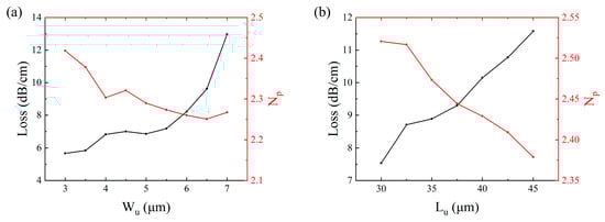
Figure 7.
RF loss and microwave refractive index under different (a) Wu and (b) Lu.
Through multi-variable parametric analysis, the geometric configuration of Wu = 6 μm and Lu = 40 μm was identified as the optimal parameter set. This selected architecture achieves precise microwave-to-optical refractive index synchronization while maintaining constrained radiofrequency dissipation characteristics. The optimized design exhibits dual performance enhancements: maintaining subcritical RF dissipation thresholds while substantially improving microwave–photonic interaction efficiency, thereby establishing essential foundations for the modulator’s broadband operational capabilities. This parametric configuration effectively balances electromagnetic confinement requirements with photonic coupling efficiency, circumventing the typical trade-off between loss suppression and interaction enhancement in conventional electrode designs.
Subsequently, our investigation conducts the systematic characterization of four critical parameters governing microwave performance in T-shaped electrode configurations. Numerical simulations were implemented to evaluate the dimensional parameters Wt and Wt1 with respect to the RF loss and refractive index characteristics. The parametric contour mapping presented in Figure 8 elucidates these geometric dependencies. Computational analysis reveals the significant intensification of the RF loss proportional to Wt1 dimensional expansion, while Wt variations demonstrate a limited correlation with the RF loss. The effective microwave refractive index exhibits coordinated augmentation with the progressive scaling of both Wt and Wt1 geometric parameters. This parametric correlation quantitatively validates the structural configuration dominance in modulating microwave propagation characteristics within the electrode system.
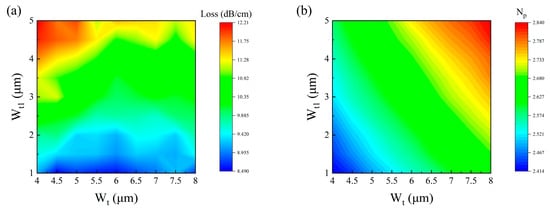
Figure 8.
Contour plots of (a) RF loss and (b) refractive index as functions of Wt and Wt1.
Through trade-off analysis based on simulation data, the geometric parameters were selected through systematic evaluation as Wt = 4 μm and Wt1 = 1 μm. This optimized configuration ensures sustained low radiofrequency dissipation while fulfilling refractive index phase-matching criteria, achieving the concurrent optimization of device integration density and fabrication process compatibility.
Similarly, systematic investigations were subsequently conducted to evaluate the dimensional dependencies of Lt and Lt1 on microwave attenuation and modal refractive index characteristics. As illustrated in Figure 9 through comprehensive parametric mapping, the electromagnetic response demonstrates pronounced geometric correlations. Computational analysis reveals distinct parametric sensitivities: Lt modifications induce marginal variations in both attenuation magnitude and refractive index distribution, while Lt1 dimension escalation produces substantial enhancement of these parameters. The optimized configuration Lt = 2 μm, Lt1 = 40 μm was derived through constrained multi-parameter optimization, achieving effective coordination between microwave propagation characteristics and time-domain response requirements while maintaining impedance compatibility.
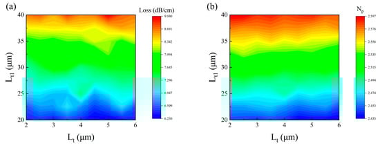
Figure 9.
Contour plots of (a) RF loss and (b) refractive index as functions of Lt and Lt1.
The optimized U-shaped electrode configuration with gap2 = 3 μm, developed through systematic parametric optimization, demonstrates a half-wave voltage-length product of 1.77 V·cm and optical propagation loss of 0.022 dB/cm when combined with calibrated photonic device parameters. These results indicate an effective reduction in optical scattering through submicron electrode geometry control and preserved modulation efficiency via coordinated microwave–optical field interactions.
3.2. Electro-Optic Modulation Bandwidth Simulation
The 3 dB bandwidth corresponds to the frequency at which the normalized response exhibits 3 dB attenuation relative to its direct current (DC) operating point, where Vin and Vpd represent the RF voltages at the modulator input and photodetector (PD) output, respectively.
Based on the wave equation and optical power correlation, the phase shift per unit propagation length exhibits a linear dependence on the output optical power under small-signal conditions. The output optical power demonstrates direct proportionality to the voltage detected by the PD. Consequently, the normalized optical power response of the modulator, termed the electro-optic (EO) response, can be expressed as follows [15,16]:
Through further derivation and simplification, Equation (6) can be reduced to the following:
where is the transmission line loss, including the conductor loss and dielectric loss, is the phase velocity mismatch factor, and L is the total length of the modulator. The is expressed as follows:
where denotes the effective microwave refractive index in the medium (), is the propagation constant, is the angular frequency, is the speed of light in vacuum, and is the effective optical refractive index in lithium niobate medium.
When the electrical phase refractive index matches the optical group refractive index (), Equation (7) can be reformulated as follows:
By setting at this point, the following can be derived from Equation (9):
The transmission characteristics of the electrical signal within the traveling-wave electrode may be characterized by the following:
Substituting Equation (10) into Equation (11) can obtain the following [17]:
Consequently, under phase velocity matching conditions where the electrical refractive index constant aligns with the optical group velocity, the 6.41 dB electrical bandwidth of the traveling-wave electrode becomes comparable to the modulator’s 3 dB electro-optic bandwidth. This equivalence allows the 6.41 dB electrical bandwidth to serve as a practical metric for estimating the modulator’s 3 dB operational bandwidth.
Under input port impedance mismatch conditions with the inclusion of reflection effects, Equation (7) undergoes modification to the following:
where Z0 is the characteristic impedance of the transmission line, Zin is the input impedance (typically 50 Ω).
Equations (7) and (13) show that the three main factors affecting the modulator bandwidth are impedance matching, microwave loss, and matching between microwave signal phase velocity and optical group velocity.
Based on the optimized parameters established in previous sections, the radiofrequency characteristics of the 0.5 cm-long modulator were numerically investigated through finite element analysis across the 1–100 GHz spectral range. Figure 10 comprehensively displays the simulated characteristic impedance profile and RF loss performance. The numerical simulations demonstrate that the modulator exhibits characteristic impedance values approximating 50 Ω in the high-frequency regime, indicating favorable impedance matching characteristics. Furthermore, the calculated RF loss is maintained below the threshold of 9.5 dB/cm throughout the entire simulated frequency domain.
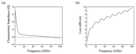
Figure 10.
(a) Characteristic impedance and (b) RF loss characteristics under a fixed device length of 0.5 cm.
The electro-optic response characteristics of the modulator were analytically derived using Equation (5). Figure 11 depicts the spectral response of the reflection coefficient along with the electro-optic modulation characteristics. Numerical evaluations indicate a modulation bandwidth surpassing 100 GHz, while the reflection coefficient is maintained below the threshold of −11 dB across the full operational bandwidth; this result satisfies the core specification, requiring a reflection coefficient of less than −10 dB in engineering applications.
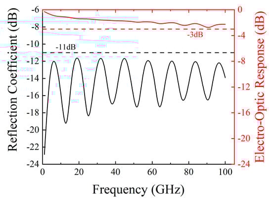
Figure 11.
Reflection coefficient and electro-optic response characteristics under a fixed device length of 0.5 cm.
4. Discussion
4.1. Comparison with LNOI Modulators in the Literature
By conducting a systematic analysis of performance metrics in recent LNOI modulator research, the electrode architecture presented in this study clearly contrasts with previous designs. As presented in Table 2, the comparison reveals that the proposed configuration retains a low value while demonstrating a modulation bandwidth surpassing 100 GHz. The innovative electrode architecture achieves optimal equilibrium between modulation efficiency and high-frequency response properties, confirming that preserving the T-shaped rail electrode configuration not only maintains its intrinsic benefits of enlarging conductor dimensions at fixed electrode spacing and minimizing ohmic dissipation [18], but also achieves enhanced device performance through the integration of an auxiliary U-shaped structural layer.
Table 2.
Performance comparison of LNOI modulators.
Although the proposed device achieves a competitive modulation bandwidth, its half-wave voltage remains suboptimal. Ongoing research focuses on minimization strategies while preserving the large bandwidth. Concurrent efforts are dedicated to advancing the modulator fabrication process. Efforts will be made to introduce improvements in the fabrication process to further optimize device performance.
4.2. Roadmap for Future Fabrication and Testing
The currently established fabrication process is shown in Figure 12. The wafer undergoes sequential cleaning using acetone, ethanol, and deionized water to remove surface contaminants. A chromium hard mask is thermally evaporated onto the lithium niobate substrate to define etch-resistant regions. Photolithography is implemented on the Cr-coated wafer to selectively remove chromium outside the optical waveguide patterns, creating the LN etch barrier. Inductively coupled plasma (ICP) etching transfers optical waveguide patterns from the chromium mask to the LN thin film [24], with subsequent Cr stripping completing the waveguide fabrication. It is noteworthy that the choice of Cr over photoresist as the hard mask for lithium niobate etching is primarily motivated by its superior etch resistance. Lithium niobate etching employs fluorine-based gases, with which Cr demonstrates an extremely low etch rate, whereas photoresist is rapidly consumed under the same conditions, resulting in pattern distortion. A Cr layer thickness of merely 120 nm suffices to effectively protect the lithium niobate layer, whereas photoresist necessitates a thickness exceeding 500 nm, thereby increasing process complexity. Furthermore, the stability of Cr enables precise control over the etch depth, preventing over-etching or sidewall tapering, thereby enhancing the fidelity of the photolithographic patterns.
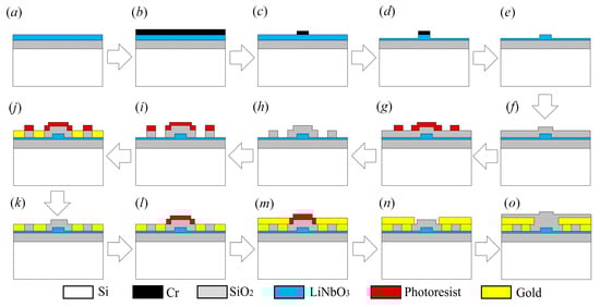
Figure 12.
Schematic diagram of TFLN modulator fabrication process. (a) Wafer cleaning; (b) Cr film deposition; (c) Cr photolithography and etching; (d) LN etching; (e) Cr stripping; (f) SiO2 deposition; (g) photoresist patterning and etching; (h) SiO2 etching and photoresist stripping; (i) photoresist patterning; (j) growth of first electrode layer; (k) photoresist stripping; (l) photoresist patterning; (m) growth of second electrode layer; (n) photoresist stripping; and (o) SiO2 passivation layer deposition.
A 800 nm-thick silicon oxide layer is deposited by plasma-enhanced chemical vapor deposition (PECVD) [25], then lithographically patterned to define metal electrode contact windows on LN. The first traveling-wave electrode is fabricated by photolithographic patterning and physical vapor deposition (PVD) with subsequent resist stripping [26]. A second metallization layer is aligned and deposited through identical sputtering processes, with thermal annealing enhancing interlayer adhesion and conductivity. An 800 nm silicon dioxide encapsulation layer is globally deposited and selectively etched to open probe contact pads at electrode terminals. Individual modulator chips are obtained through wafer dicing and optical facet polishing processes.
Figure 13 illustrates the configuration of the measurement system, employing a 1550 nm wavelength laser source fiber-coupled to the modulator. A signal generator externally generates a 1 kHz triangular wave spanning from 0 V to beyond twice the value, which is then delivered to the traveling-wave electrode. The triangular wave amplitude is precisely tuned to surpass double the threshold. The generated triangular wave is split into two branches, with one branch feeding the traveling-wave electrode while the other serves as the oscilloscope reference. The modulator’s optical output passes through a photodetector for optical-to-electrical conversion prior to oscilloscope acquisition. A 0–10 V triangular wave amplitude range establishes a linear periodic voltage excitation (0–10 V) across the modulator’s electrodes; this configuration results in periodic optical output from the modulator. The voltage difference in the triangular wave amplitude required to induce a π-phase shift in the oscilloscope-measured output directly determines the value.
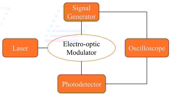
Figure 13.
Schematic of the characterization setup for thin-film lithium niobate modulators.
Figure 14 illustrates the characterization system for insertion loss and extinction ratio measurements, configured with a 1550 nm wavelength laser source. The traveling-wave electrode is biased using a DC source implementing a voltage sweep from −5 V to +5 V with 0.1 V increments. An optical power meter monitors the modulator’s output to record the voltage-dependent optical power variations, the extinction ratio (in dBm) is calculated as the power difference between the maximum and minimum transmission states, and the maximum and minimum power levels generally appear around 0 V bias and the half-wave voltage point. A reference optical power measurement is performed at the modulator’s input using the same power meter. The insertion loss corresponds to the difference between the input optical power and maximum transmitted output power.
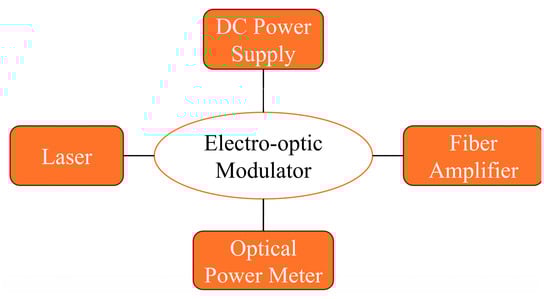
Figure 14.
Schematic of the extinction ratio and insertion loss characterization setup for thin-film lithium niobate modulators.
Figure 15 presents the measurement configurations for S-parameter characterization and EO response evaluation. As illustrated in Figure 15a, S-parameter measurements are performed by directly connecting the modulator’s RF input and output ports to a vector network analyzer (VNA), with no optical signal path required. The EO response measurement setup in Figure 15b employs a 1550 nm laser source coupled to the optical modulator. The modulated optical output is amplified by an erbium-doped fiber amplifier (EDFA), then converted to an electrical signal through a photodetector for VNA signal acquisition, and the RF input port is connected to the VNA’s test port. The output port is terminated with a 50 Ω impedance-matched load and a DC bias voltage, optimized for the modulator’s linear operating regime, is applied to the DC bias electrode through a dedicated power supply, and RF modulation signals from the VNA and DC bias are combined via a bias tee, then jointly applied to the traveling-wave electrode structure.
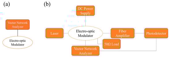
Figure 15.
Schematic of the (a) S-parameters and (b) EO response characterization setup for thin-film lithium niobate modulators.
5. Conclusions
In this work, we demonstrate a TFLN modulator featuring an innovative U-T-shaped dual-layer traveling-wave electrode architecture. Systematic optimization combining theoretical analysis and electromagnetic simulations achieves a of 1.77 V·cm, a modulation bandwidth exceeding 100 GHz, and optical propagation loss below 0.022 dB/cm, which collectively demonstrate the device’s superior electro-optic performance. This configuration establishes a novel design paradigm for electrode architectures in TFLN-based modulators. Additionally, we outline preliminary fabrication processes and testing methodologies, establishing a clear roadmap for future implementation.
Author Contributions
Conceptualization, Y.H.; methodology, Y.H.; software, Y.H. and H.L. (Haisheng Li); validation, Y.H. and H.L. (Haiou Li); formal analysis, Y.H.; investigation, Y.L. (Yingbo Liu); resources, H.L. (Haiou Li); data curation, L.Q. and J.Y.; writing—original draft preparation, Y.H.; writing—review and editing, Y.H.; visualization, Y.L. (Yue Li); supervision, Y.L. (Yue Li); project administration, H.L. (Haisheng Li); funding acquisition, H.L. (Haiou Li). All authors have read and agreed to the published version of the manuscript.
Funding
This research was funded by National Natural Science Foundation of China (No. 62174041); Guangxi Science and Technology Plan Project (AD24010060); and Guangxi Science and Technology Base and Talent Special Project (Guike AD24010060).
Institutional Review Board Statement
Not applicable.
Informed Consent Statement
Not applicable.
Data Availability Statement
The data presented in this study are available upon request from the corresponding author.
Acknowledgments
We thank the National Natural Science Foundation of China, the Guangxi Natural Science Foundation, the GUET Graduate Education Innovation Project for partial funding, and the National Key R&D Program of China.
Conflicts of Interest
Authors Yue Li, Liangpeng Qin, Haisheng Li were employed by the company The 34th Research Institute of China Electronics Technology Group Corporation. The remaining authors declare that the research was conducted in the absence of any commercial or financial relationships that could be construed as potential conflicts of interest.
References
- Azadeh, S.S.; Merget, F.; Romero-García, S.; Moscoso-Mártir, A.; von den Driesch, N.; Müller, J.; Mantl, S.; Buca, D.; Witzens, J. Low Vπ Silicon photonics modulators with highly linear epitaxially grown phase shifters. Opt. Express 2015, 23, 23526–23550. [Google Scholar] [CrossRef]
- Ogiso, Y.; Ozaki, J.; Ueda, Y.; Kashio, N.; Kikuchi, N.; Yamada, E.; Tanobe, H.; Kanazawa, S.; Yamazaki, H.; Ohiso, Y.; et al. Over 67 GHz Bandwidth and 1.5 V Vπ InP-Based Optical IQ Modulator with n-i-p-n Heterostructure. J. Light. Technol. 2017, 35, 1450–1455. [Google Scholar] [CrossRef]
- Wolf, S.; Zwickel, H.; Kieninger, C.; Lauermann, M.; Hartmann, W.; Kutuvantavida, Y.; Freude, W.; Randel, S.; Koos, C. Coherent modulation up to 100 GBd 16QAM using silicon-organic hybrid (SOH) devices. Opt. Express 2018, 26, 220–232. [Google Scholar] [CrossRef] [PubMed]
- Noguchi, K.; Mitomi, O.; Miyazawa, H. Millimeter-wave Ti:LiNbO3 optical modulators. J. Light. Technol. 1998, 16, 615–619. [Google Scholar] [CrossRef]
- Wooten, E.L.; Kissa, K.M.; Yi-Yan, A.; Murphy, E.J.; Lafaw, D.A.; Hallemeier, P.F.; Maack, D.; Attanasio, D.V.; Fritz, D.J.; McBrien, G.J.; et al. A review of lithium niobate modulators for fiber-optic communications systems. IEEE J. Sel. Top. Quantum Electron. 2000, 6, 69–82. [Google Scholar] [CrossRef]
- Li, M.; Wang, L.; Li, X.; Xiao, X.; Yu, S. Silicon intensity Mach–Zehnder modulator for single lane 100 Gb/s applications. Photonics Res. 2018, 6, 109–116. [Google Scholar] [CrossRef]
- Ogiso, Y.; Hashizume, Y.; Tanobe, H.; Nunoya, N.; Ida, M.; Miyamoto, Y.; Ishikawa, M.; Ozaki, J.; Ueda, Y.; Wakita, H.; et al. 80-GHz Bandwidth and 1.5-V Vπ InP-Based IQ Modulator. J. Light. Technol. 2020, 38, 249–255. [Google Scholar] [CrossRef]
- Hou, S.; Hu, H.; Liu, Z.; Xing, W.; Zhang, J.; Hao, Y. High-Speed Electro-Optic Modulators Based on Thin-Film Lithium Niobate. Nanomaterials 2024, 14, 867. [Google Scholar] [CrossRef] [PubMed]
- Wang, C.; Zhang, M.; Chen, X.; Bertrand, M.; Shams-Ansari, A.; Chandrasekhar, S.; Winzer, P.; Loncar, M. Integrated lithium niobate electro-optic modulators operating at CMOS-compatible voltages. Nature 2018, 562, 101–104. [Google Scholar] [CrossRef]
- Liu, X.; Xiong, B.; Sun, C.; Wang, J.; Hao, Z.; Wang, L.; Han, Y.; Li, H.; Yu, J.; Luo, Y. Wideband thin-film lithium niobate modulator with low half-wave-voltage length product. Chin. Opt. Lett. 2021, 19, 060016. [Google Scholar] [CrossRef]
- Chen, G.; Chen, K.; Gan, R.; Ruan, Z.; Wang, Z.; Huang, P.; Lu, C.; Lau, A.P.T.; Dai, D.; Guo, C.; et al. High performance thin-film lithium niobate modulator on a silicon substrate using periodic capacitively loaded traveling-wave electrode. APL Photonics 2022, 7, 026103. [Google Scholar] [CrossRef]
- Xingrui, H.; Yang, L.; Donghe, T.; Zhiguo, Y.; Qingquan, W.; Zhiyong, L. Linearity-Enhanced Dual-Parallel Mach–Zehnder Modulators Based on a Thin-Film Lithium Niobate Platform. Photonics 2022, 9, 197. [Google Scholar]
- Jian, J.; Mengyue, X.; Liu, L.; Yannong, L.; Junwei, Z.; Lin, L.; Lidan, Z.; Hui, C.; Siyuan, Y.; Xinlun, C. High modulation efficiency lithium niobate Michelson interferometer modulator. Opt. Express 2019, 27, 18731–18739. [Google Scholar] [CrossRef]
- Arizmendi, L. Photonic applications of lithium niobate crystals. Phys. Status Solidi (A) 2004, 201, 253–283. [Google Scholar] [CrossRef]
- Yachao, J.; Guofang, F.; Rongwei, W.; Zeping, Z.; Muguang, W.; Xiaoyu, C.; Jiasi, W.; Xin, C.; Hongyu, L.; Yuan, L. Analysis for an improved nanomechanical microcantilever sensor on optical waveguides. IEEE Access 2020, 8, 63856–63861. [Google Scholar]
- Chung, H.Y.; Chang, W.S.C.; Adler, E.L. Modeling and optimization of traveling-wave LiNbO3 interferometric modulators. IEEE J. Quantum Electron. 1991, 27, 608–617. [Google Scholar] [CrossRef]
- Kubota, K.; Noda, J.; Mikami, O. Traveling wave optical modulator using a directional coupler LiNbO3waveguide. IEEE J. Quantum Electron. 1980, 16, 754–760. [Google Scholar] [CrossRef]
- Kharel, P.; Reimer, C.; Luke, K.; He, L.; Zhang, M. Breaking voltage-bandwidth limits in integrated lithium niobate modulators using micro-structured electrodes. Optica 2021, 8, 357–363. [Google Scholar] [CrossRef]
- Yang, T.; Cai, L.; Huang, Z.; Zhang, L. High-Linearity Dual-Parallel Mach–Zehnder Modulators in Thin-Film Lithium Niobate. Photonics 2024, 11, 987. [Google Scholar] [CrossRef]
- Luo, X.; Gu, Z.; Wang, C.; Fan, C.; Zhang, W. Large-Bandwidth Lithium Niobate Electro-Optic Modulator for Frequency-Division Multiplexing RFID Systems. Electronics 2024, 13, 5054. [Google Scholar] [CrossRef]
- Liu, Y.; Li, H.; Liu, J.; Tan, S.; Lu, Q.; Guo, W. Low Vπ thin-film lithium niobate modulator fabricated with photolithography. Opt. Express 2021, 29, 10. [Google Scholar] [CrossRef] [PubMed]
- Du, Y.; Zou, X.; Zou, F.; Pan, W.; Yan, L.; Zhao, Q.; Liu, N. Novel Folded Structure TFLN Recycling Phase Modulator Enabling Large Low-Vπ Bandwidth and Efficient Microwave–Optical Velocity Matching. Laser Photonics Rev. 2024, 18, 2400787. [Google Scholar] [CrossRef]
- Wang, M.; Qi, L.; Wang, H.; Ruan, Z.; Chen, G.; Chen, B.; Gong, S.; Chen, K.; Liu, L. Robust thin-film lithium niobate modulator on a silicon substrate with backside holes. Chin. Opt. Lett. 2024, 22, 050601. [Google Scholar] [CrossRef]
- Batsala, M.; Chandu, B.; Sakala, B.; Nama, S.; Domatoti, S. Inductively coupled plasma mass spectrometry (ICP-MS). Int. J. Res. Pharm. Chem. 2012, 27, 1181–1184. [Google Scholar]
- Yi, K.; Liu, D.; Chen, X.; Yang, J.; Wei, D. Plasma-Enhanced Chemical Vapor Deposition of Two-Dimensional Materials for Applications. Acc. Chem. Res. 2021, 54, 1011–1022. [Google Scholar] [CrossRef]
- Deng, Y.; Chen, W.; Li, B.; Wang, C.; Li, Y. Physical vapor deposition technology for coated cutting tools: A review. Ceram. Int. 2020, 46, 18373–18390. [Google Scholar] [CrossRef]
Disclaimer/Publisher’s Note: The statements, opinions and data contained in all publications are solely those of the individual author(s) and contributor(s) and not of MDPI and/or the editor(s). MDPI and/or the editor(s) disclaim responsibility for any injury to people or property resulting from any ideas, methods, instructions or products referred to in the content. |
© 2025 by the authors. Licensee MDPI, Basel, Switzerland. This article is an open access article distributed under the terms and conditions of the Creative Commons Attribution (CC BY) license (https://creativecommons.org/licenses/by/4.0/).