Communication

An All-Optical Plasmon Modulator with a High Extinction Ratio Based on the Resonance of a Silver Block

1
College of Digital Technology and Engineering, Ningbo University of Finance & Economics, Ningbo 315175, China
2
Department of Global Convergence, Kangwon National University, 1 Gangwondaehak-gil, Chuncheon-si 24341, Gangwon-do, Republic of Korea
3
Advanced Photonics Center, School of Electronic Science & Engineering, Southeast University, Nanjing 210018, China
4
School of Information Technology, Jiangsu Open University, Nanjing 210036, China
*
Author to whom correspondence should be addressed.
Photonics 2025, 12(7), 646; https://doi.org/10.3390/photonics12070646
Submission received: 1 June 2025 / Revised: 19 June 2025 / Accepted: 24 June 2025 / Published: 25 June 2025

Abstract

Conventional all-optical modulators based on surface plasmon polaritons (SPPs) primarily utilize the nonlinear effect of a given material for modulation. Their performance is heavily dependent on the optical properties of the dielectric materials used and requires high pumping power. However, manipulating SPPs by controlling electron concentrations offers a material-independent approach suitable for all-optical modulators. In this paper, we propose a hybrid gold–ITO–silver block structure integrated within a Mach–Zehnder interferometer configuration to address this problem. The gold–ITO interface effectively localizes propagating SPPs. The pump light excites localized surface plasmons (LSPs) in the silver block, generating surface electric fields that modulate the electron concentration in the adjacent ITO layer. The extinction ratio is 50.8 dB when the electron concentration changes by 3.3 × 1020 cm−3, indicating that this structure is an all-optical modulator with a high extinction ratio. This approach shows significant promise for reducing pump power and enhancing the performance of all-optical modulators.

1. Introduction

Surface plasmon polaritons (SPPs), collective oscillation-mode particles formed through strong coupling between free electrons and electromagnetic fields at metal–dielectric interfaces, fundamentally arise from energy exchange between optical fields and surface electron dynamics [1,2,3,4]. These unique electromagnetic modes enable subwavelength optical confinement transcending the diffraction limit of conventional optics while maintaining both photonic propagation characteristics and electronic localization along interfaces. This dual nature inspires novel physical mechanisms for the manipulation of light at nanoscale dimensions [5,6,7,8,9,10]. SPP-based all-optical modulation technology directly manipulates optical signal properties through purely optical means, circumventing the bottlenecks inherent in traditional opto-electronic conversion within communication systems. This approach fundamentally overcomes the intrinsic speed limitations imposed by electronic components while also reducing the substantial energy consumption associated with the opto-electronic conversion process [11,12,13,14]. SPP-based all-optical modulation provides a crucial technological underpinning for constructing next-generation intelligent all-optical networks characterized by low latency and low power consumption [15,16,17,18]. Hence, an effective control method for all-optical modulators based on SPPs would be of great significance.
The propagation of SPPs is intrinsically linked to electron concentrations, making modulation via electron concentration a significant research direction. This approach offers a novel optical modulation mechanism independent of dielectric materials [19,20]. On the one hand, the strong coupling between surface charges and optical fields in plasmonic structures enables enhanced modulation efficiency and reduced pump power through electron concentration control. On the other hand, this material-independent modulation strategy exhibits greater compatibility with established integrated photonic systems and fabrication processes [21]. For instance, Kevin et al. developed an ultrafast all-optical modulator by modulating the electron concentration on an aluminum surface using pump light. However, this method exhibited limited modulation efficiency, achieving an only 7.5% modulation in the intensity of SPPs under an optical fluence of 10 mJ·cm−3, primarily due to the inherent difficulty of modulating electron concentrations on metal surfaces [22]. Indium tin oxide (ITO), a transparent semiconducting material, plays a pivotal role in semiconductor integration and optical communication owing to its high conductivity and voltage-tunable properties [23,24,25,26]. In 2023, Swati et al. proposed an innovative approach for all-optical modulation using an ITO-based vertically coupled ring resonator. This method leveraged the material’s enhanced nonlinear response, particularly in the epsilon-near-zero regime at near-infrared wavelengths, achieving a high extinction ratio (ER) of 18 dB in a device 30 µm long [27]. Nevertheless, the modulation performance of this technique remains primarily dependent on dielectric properties and shows great room for improvement. For all-optical modulators, directly modulating ITO electron concentrations via the localized electric field of a metal structure holds significant promise for enhancing device performance and advancing integration capabilities [28,29].
In this paper, we propose an all-optical modulator based on localized surface plasmon resonance in metallic structures. The device integrates a Mach–Zehnder interferometer (MZI) comprising metal and ITO components, featuring thin silver blocks patterned on both the upper and lower arms. Counter-propagating pump beams selectively excite localized surface plasmons (LSPs) within these silver blocks, leveraging the resultant electric field enhancement to modulate the electron concentration in the ITO layer. This modulation strategy offers significant advantages in achieving high-ER and low-power operation, demonstrating considerable potential for applications in optoelectronic sensing, optical communications, and photodetection systems [30,31,32,33].

2. Analysis of the Models

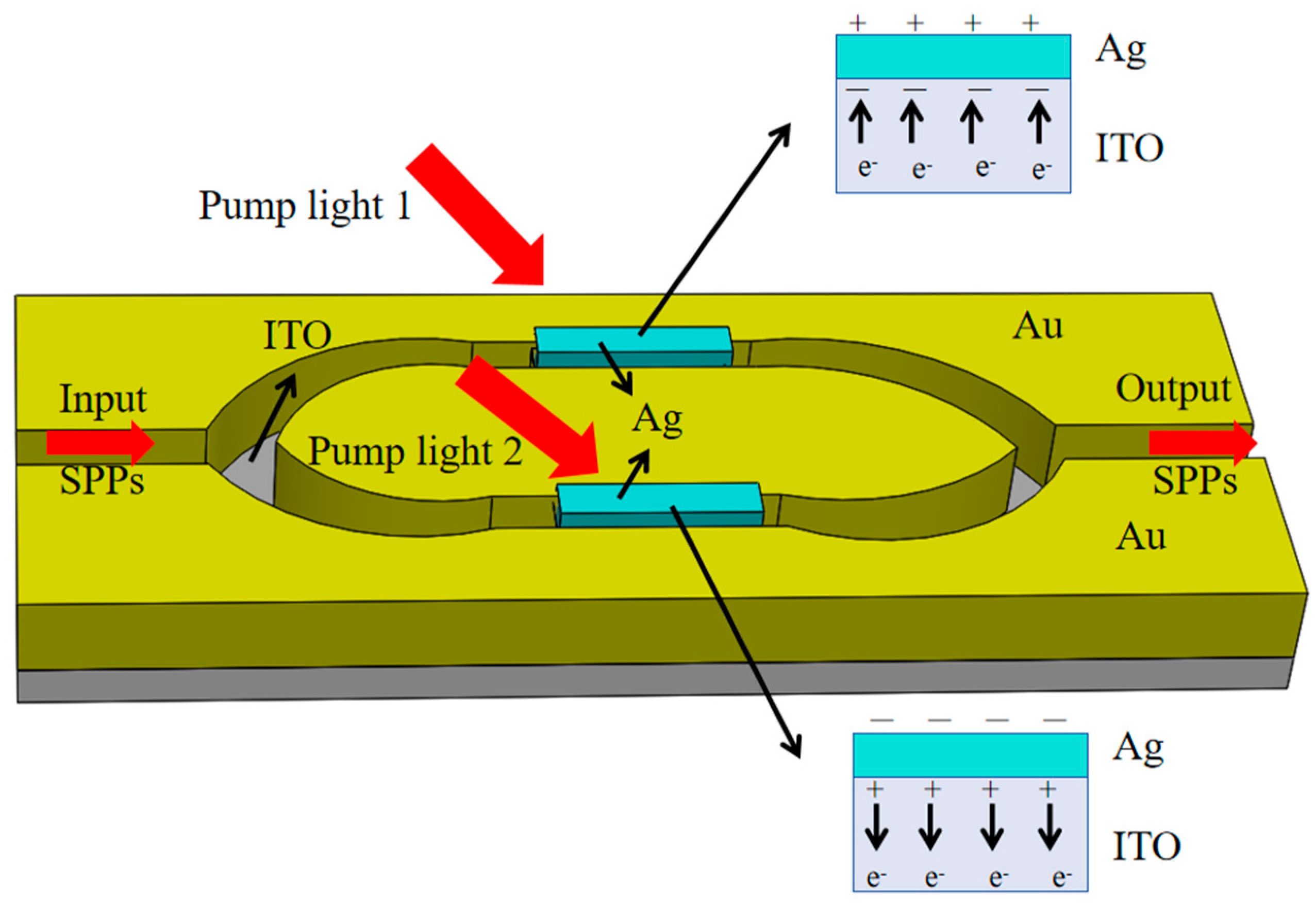
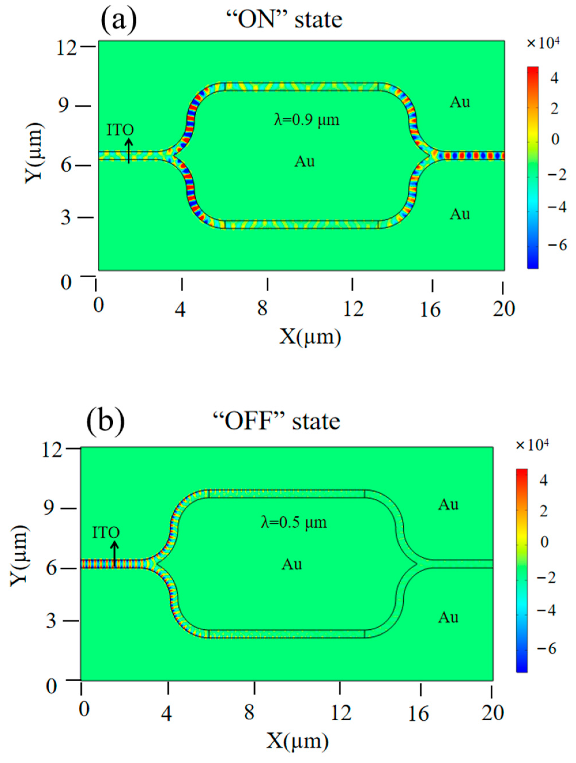
2.1. Three-Dimensional Model

The three-dimensional model of our proposed structure, illustrated in Figure 1, features an MZI structure comprising gold (Au) and an ITO waveguide. A rectangular silver block is employed on the arm of the ITO layer. The proposed structure can be fabricated by means of traditional photolithography and metal lift-off technology. The Au-ITO interface confines the propagating SPPs effectively. The pump light is split into two beams with a π-phase shift; the two beams independently excite LSPs within the rectangular silver blocks in the upper and lower arms. This process generates localized electric fields with opposite polarity, inducing opposite changes in the electron concentration of the modulation ITO. Then, the refractive index of the ITO is modulated (the influence of temperature is neglected as the purpose of the structure is to realize high-speed modulation in an all-optical modulator, while heat affects the ITO’s properties much more slowly than light control affects electron concentrations). The subsequent interference of the recombined SPPs at the output port enables all-optical modulation of the transmitted SPPs’ signal. Through localized field enhancement, this modulation strategy significantly reduces pump power, facilitating low-power all-optical control. Furthermore, as SPPs across different wavelengths can be modulated via electron concentration tuning, this approach theoretically enables broadband all-optical modulation.

2.2. Simulation Model

To reduce computational burden and enhance simulation efficiency, we employed a two-dimensional model for simulation that considered the inherent symmetry of the structure, as depicted in Figure 2. The length, width, and height of waveguide were 20 μm, 12 μm, and 400 nm, respectively. SPPs were excited at the input port and propagated along the Au-ITO interface, as the working wavelength of SPPs was set to 1.2 μm. A dedicated ITO modulation region was placed within the arm of the MZI, with its dimensions determined by the size of the silver block. Upon excitation of LSPs on the silver blocks, the enhanced local electric fields modulate the electron concentration of the ITO. The modulation of the SPPs was effectively characterized by analyzing the electric field distribution, optical transmission, and phase shift within the model. This study systematically analyzes the influence of ITO electron concentration, silver block length, and working wavelength. The relationship between the refractive index of ITO and electron concentrations is reported in reference [34], where it is stated that the corresponding real part (n) and imaginary part (k) of the effective refractive index at different electron concentrations can be calculated for simulation. The effective index of the waveguide changes when the electron concentration or the wavelength of the SPPs is modified, and the height of ITO is not taken into consideration as its impact on the propagating SPPs is not significant in this model [35].

3. Analysis of Simulation Results

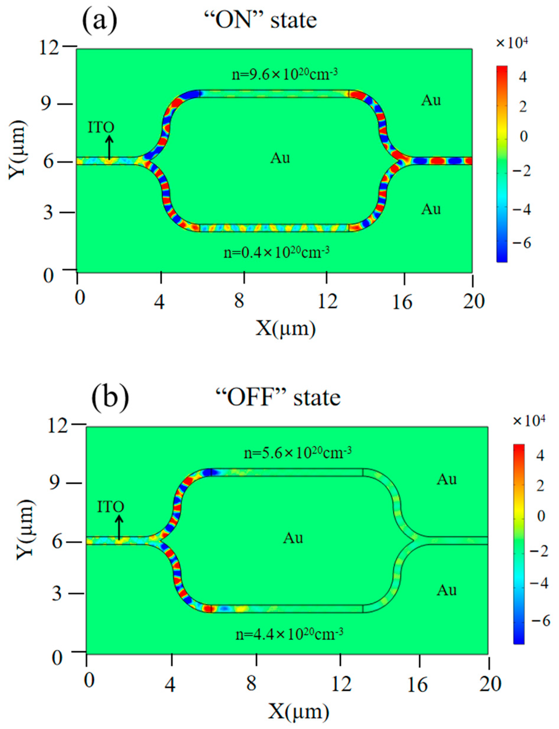
3.1. Different Electron Concentrations

3.1.1. Electric Field Distribution

Variations in pump light excitation efficiency lead to differences in the magnitude of the localized electric field associated with LSPs. This, in turn, induces corresponding changes in the electron concentration of the ITO layer. Therefore, we analyzed the modulation effects that occur with different ITO electron concentrations of the arms. Figure 3a depicts the x component of the electric field distribution when the electron concentrations in the upper and lower arms are 0.4 × 1020 cm3 and 9.6 × 1020 cm3, respectively, with the electron concentration in other regions maintained at 5 × 1020 cm3. Under these conditions, a clear SPPs signal can be observed at the output port (ON state). Conversely, Figure 3b shows the x component of the electric field distribution when the electron concentrations in the upper and lower arms are 4.4 × 1020 cm3 and 5.6 × 1020 cm3, respectively. The SPP signal is virtually undetectable at the output port (OFF state), demonstrating a distinct switching effect. These results confirm that modulating the electron concentration is an effective way to control the propagating SPPs.

3.1.2. Optical Transmission

The optical transmission of the propagating SPPs at the output port was characterized to further analyze the modulation performance of the device. Figure 4 shows optical transmission as a function of electron concentration. The reference electron concentration of ITO was set to 5.0 × 1020 cm−3, while the electron concentrations of the upper and lower arms were set to (5 + N) × 1020 cm−3 and (5-N) × 1020 cm−3, respectively. The optical transmission is −54.8 dB when the value of N is 1.4. The optical transmission reaches −4.0 dB when N increases to 4.7, with a corresponding ER of 50.8 dB. This significant variation in optical transmission arises from the phase difference between the SPPs propagating in the upper and lower arms, a difference induced by their differing electron concentrations. The interference at the output port causes either constructive or destructive superposition of the electric fields, leading to the observed enhancement or attenuation of the transmitted signal.

3.1.3. Phase Shift

Variations in electron concentration modify the refractive index of ITO, thereby altering the optical path of propagating SPPs. Consequently, we analyzed the phase shift at the output port of the model for different electron concentrations, as shown in Figure 5. The phase is −179° when the value of N is 2. The phase shifts to 164° when N increases to 3.8, representing a total phase change of 343°. This significant phase shift demonstrates effective control over the phases of propagating SPPs through active electron concentration tuning. The resulting phase difference enables interference at the output port, facilitating the observed switching behavior.

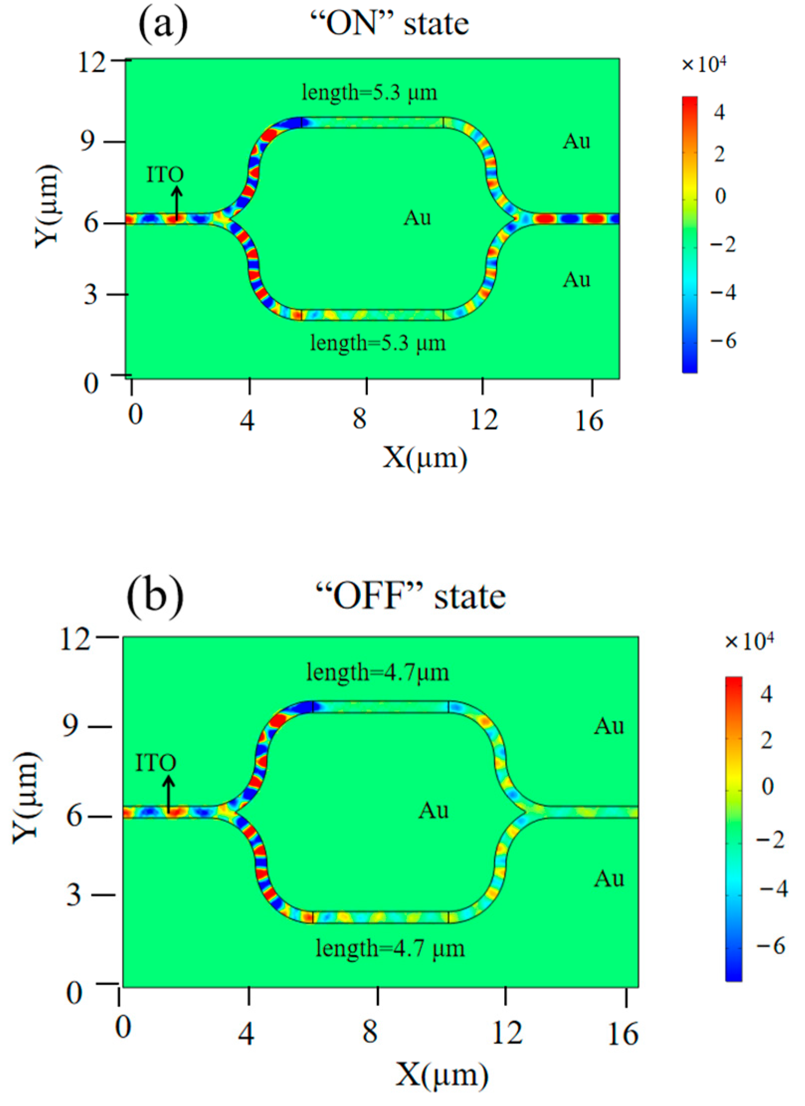
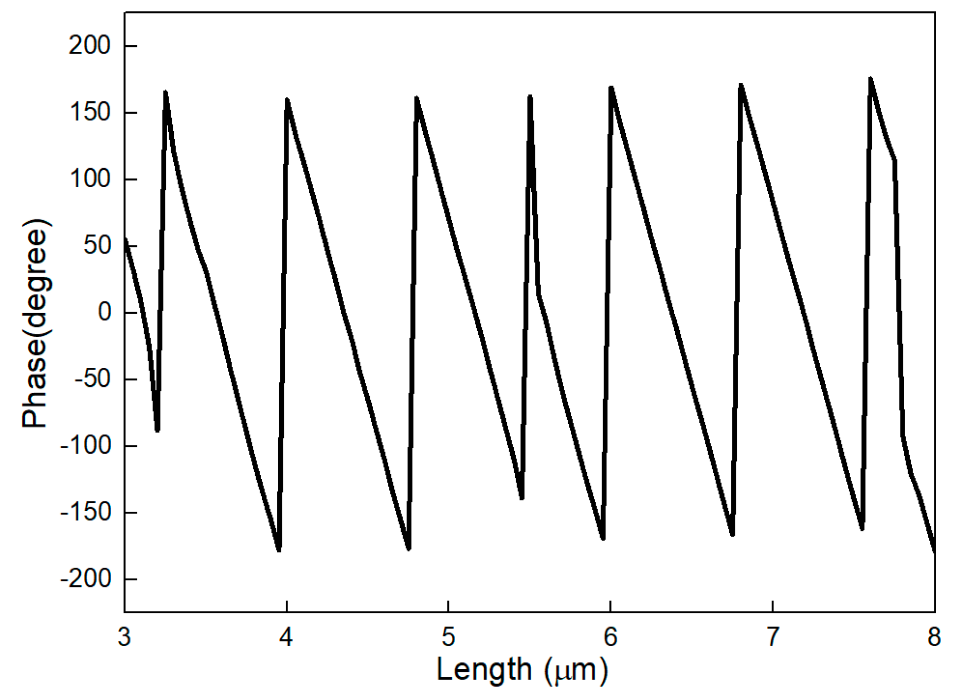
3.2. Different Silver Block Lengths

3.2.1. Electric Field Distribution

The length of the silver blocks significantly influences the modulation region of the ITO, consequently affecting the propagating SPPs. We characterized the modulation performance at various block lengths. Figure 6a depicts the x component electric field distribution for a block length of 5.3 μm. Under these conditions, a distinct SPP field distribution can clearly be observed at the output port (ON state). In contrast, Figure 6b shows the x component of the electric field distribution when the block length is decreased to 4.7 μm. The SPP signal is essentially undetectable at the output port (OFF state), demonstrating effective switching behavior. These results confirm that the length of the silver blocks provides an effective means of modulating propagating SPPs.

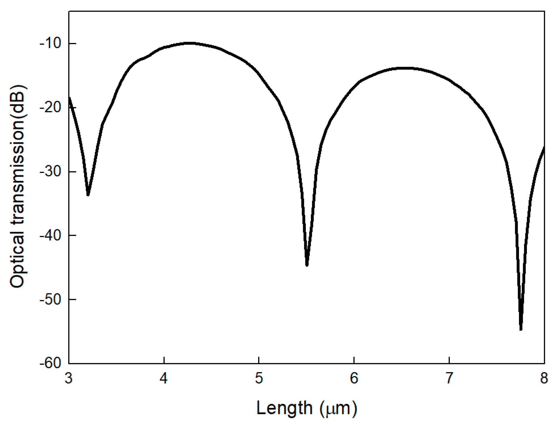
3.2.2. Optical Transmission

To further quantify the modulation performance of the device, we analyzed the optical transmission of propagating SPPs under the influence of different silver block lengths. Figure 7 displays the optical transmission versus various silver block lengths. The optical transmission is −9.9 dB at a block length of 4.2 μm. However, the optical transmission decreases significantly to −54.6 dB when the length of the block increases to 7.7 μm, yielding an ER of 44.5 dB. This substantial difference in optical transmission is ascribed to the phase mismatch of SPPs propagating along the upper and lower arms, a result of the disparity in the lengths of the silver blocks. Thus, constructive and destructive interference at the output port lead to localized electric field enhancement or attenuation, thereby modulating optical transmission.

3.2.3. Phase Shift

Silver block length directly influences the optical path of propagating SPPs. So, we characterized the phase variation occurring with different lengths of the silver blocks, as shown in Figure 8. The phase is −178° when the length of the silver block is 3.9 μm, while the phase shifts to 175° when the length increases to 7.6 μm, a corresponding total phase shift of 353°. This demonstrates that silver block length can also effectively modulate the phases of propagating SPPs. The controllable constructive and destructive interference at the output port thus enable switching functionality.

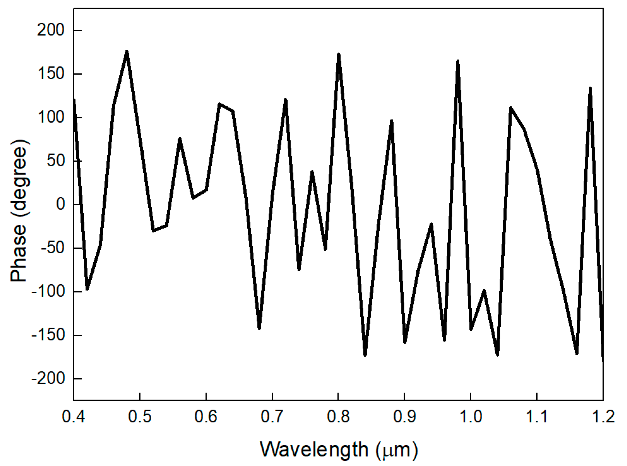
3.3. Different Working Wavelengths

3.3.1. Electric Field Distribution

The modulation efficiency of SPPs exhibits significant wavelength dependence during propagation. To characterize this phenomenon, we simulated the electric field distributions under different working wavelengths of SPPs. Figure 9a displays the x component’s electric field distribution at a wavelength of 0.9 μm, indicating that a discernible SPP field distribution emerges at the output port (ON state). In contrast, Figure 9b shows a negligible SPP signal at the output port when the wavelength decreases to 0.5 μm (OFF state), demonstrating a pronounced switching functionality. These distinct modulation characteristics validate the wavelength-selective response of the structure we designed.

3.3.2. Optical Transmission

To further investigate the wavelength-dependent modulation characteristics of the device, we analyzed the optical transmission of propagating SPPs as a function of wavelength. Figure 10 presents the optical transmission versus different wavelengths. The optical transmission is −54.5 dB at a wavelength of 0.46 μm. Conversely, the optical transmission rises to −9.0 dB when the wavelength increases to 0.8 μm, yielding a ER of 45.5 dB. This significant contrast is primarily ascribed to the different influences of electron concentration on the different propagating wavelengths of SPPs.

3.3.3. Phase Shift

The optical path for the propagating SPPs in ITO exhibits wavelength-dependent variations. To quantify this effect, we characterized the phase response across different wavelengths, as presented in Figure 11. The phase is 176° when the wavelength of the SPPs is 0.48 μm. The phase shifts to −172° when the wavelength increases to 0.84 μm, corresponding to a cumulative phase shift of 348°. Although the change in wavelength is small, the change in phase is significant, as the electron concentrations of both arms are well optimized and set for the highest ER. This near-cycle phase modulation demonstrates the strong wavelength-selective phase modulation capability of the structure we designed.

3.3.4. Optical Transmission Versus Different Wavelengths and Electron Concentrations

The operational principle of our modulator is based on electron concentration tuning, which serves as a wavelength-independent control mechanism. This fundamental characteristic enables broadband operation across a wide spectral range. To evaluate this capability, we systematically scanned working wavelengths from 0.4 μm to 1.2 μm. Figure 12 presents the corresponding optical transmission at different electron concentrations, demonstrating significant modulation of propagating SPPs at various electron concentrations throughout the investigated bandwidth. These findings theoretically prove that the proposed model can also realize bandwidth modulation.
In Table 1, the proposed modulator is compared with other all-optical modulators from other studies in terms of ER. The proposed structure presents significant advantages in ER owing to the fact that it achieves modulation via directly controlling the concentration of electrons.

4. Conclusions

In conclusion, we propose an all-optical plasmonic modulator based on a hybrid MZI architecture comprising silver blocks integrated with an ITO waveguide. In this design, pump-light-excited LSPs in silver blocks are used to dynamically tune the electron concentration of ITO. The resultant phase modulation of propagating SPPs induces controllable constructive/destructive interference at the output port, achieving high-performance switching functionality with a high extinction ratio of 50.8 dB. Both the electron concentration and silver block geometry give rise to versatile tuning knobs for manipulating guided SPP propagation. This platform demonstrates significant potential for photonic integrated circuits, including applications in optical communications, photodetection, and high-sensitivity biosensing.

5. Methods

The simulation was performed using the commercial finite element method (FEM) and the trial version of the software product “COMSOL Multiphysics 5.5”. In the simulation, scattering boundary conditions and a user-defined port were used, and the SPPs were excited using port mode. A radio frequency module was used to investigate the relationship between different parameters and the optical transmission and electric field distribution.

Author Contributions

C.L. and S.Y. designed the study, J.F. performed the numerical simulation, and M.L. and X.H. interpreted the results and wrote the manuscript. All authors have read and agreed to the published version of the manuscript.

Funding

This work was supported in part by the National Natural Science Foundation of China (NSFC) (12274075).

Institutional Review Board Statement

Not applicable.

Informed Consent Statement

Not applicable.

Data Availability Statement

The data related to the experiments discussed in this work are available upon reasonable request from the corresponding author Sisi Yang.

Conflicts of Interest

The authors declare no conflicts of interest.

References

  1. AlAloul, M.; Rasras, M. Low insertion loss plasmon-enhanced graphene all-optical modulator. ACS Omega 2021, 6, 7576–7584. [Google Scholar] [CrossRef] [PubMed]
  2. Xing, J.; Sun, C.; Xiong, B.; Wang, J.; Hao, Z.; Wang, L.; Han, Y.; Li, H.; Yu, J.; Luo, Y. Low loss hybrid plasmon polariton Mach-Zehnder modulators. OSA Contin. 2021, 4, 2721–2733. [Google Scholar] [CrossRef]
  3. Cao, Z.; Lin, H.; Cheng, Y.; Xu, Y.; Gong, Q.; Lü, G. Light-field modulation and optimization near metal nanostructures utilizing spatial light modulators. Chin. Phys. B 2024, 33, 104201. [Google Scholar] [CrossRef]
  4. Švanda, J.; Kalachyova, Y.; Mareš, D.; Siegel, J.; Slepička, P.; Kolská, Z.; Macháč, P.; Michna, Š.; Švorčík, V.; Lyutakov, O. Smart Modulators Based on Electric Field-Triggering of Surface Plasmon–Polariton for Active Plasmonics. Nanomaterials 2022, 12, 3366. [Google Scholar] [CrossRef]
  5. Yang, F.; Bi, Z.Y.; Zhang, H.; Fu, Z.Y.; Liu, C.X.; Fu, X.J.; Wu, J.W.; Ma, H.F. Quadrature-Phase-Shift-Keying Direct Modulator Based on Spoof Surface-Plasmon Polaritons. Phys. Rev. Appl. 2023, 20, 014049. [Google Scholar] [CrossRef]
  6. Ramírez, A.P.; Zhai, T.; Salas-Montiel, R.; Cortés, V.R. Dynamic tailoring large-area surface plasmon polariton excitation. J. Opt. 2024, 26, 115003. [Google Scholar] [CrossRef]
  7. Zhou, F. A broadband modulator based on graphene/black phosphorus heterostructure with enhanced modulation depth. Heliyon 2024, 10, e34684. [Google Scholar] [CrossRef]
  8. Barbillon, G. Latest Advances in Nanoplasmonics and Use of New Tools for Plasmonic Characterization. Photonics 2022, 9, 112. [Google Scholar] [CrossRef]
  9. Zhang, Z.; Yang, J.; He, X.; Han, Y.; Zhang, J.; Huang, J.; Chen, D.; Xu, S. Active enhancement of slow light based on plasmon-induced transparency with gain materials. Materials 2018, 11, 941. [Google Scholar] [CrossRef]
  10. Zhang, Z.; Yang, J.; Bai, W.; Han, Y.; He, X.; Zhang, J.; Huang, J.; Chen, D.; Xu, S.; Xie, W. Chipscale plasmonic modulators and switches based on metal–insulator–metal waveguides with Ge2Sb2Te5. J. Nanophotonics 2019, 13, 046009. [Google Scholar] [CrossRef]
  11. Yang, H.; Wang, Y.; Tiu, Z.C.; Tan, S.J.; Yuan, L.; Zhang, H. All-optical modulation technology based on 2D layered materials. Micromachines 2022, 13, 92. [Google Scholar] [CrossRef] [PubMed]
  12. Wang, H.; Niu, J.; Chen, Q.; Zhao, S.; Shao, H.; Yang, Y.; Chen, H.; Li, S.; Qian, H. All-optical modulator with photonic topological insulator made of metallic quantum wells. Nanophotonics 2024, 13, 3575–3580. [Google Scholar] [CrossRef] [PubMed]
  13. Yuan, J.; Dong, S.; Zhang, H.; Wu, C.; Wang, L.; Xiao, L.; Jia, S. Efficient all-optical modulator based on a periodic dielectric atomic lattice. Opt. Express 2021, 29, 2712–2719. [Google Scholar] [CrossRef]
  14. Li, Z.; Chen, J.; Ma, Z.; Tang, C.; Sua, Y.M.; Huang, Y.P. Parametric all-optical modulation on a chip. Phys. Rev. Appl. 2024, 21, 064049. [Google Scholar] [CrossRef]
  15. Basiri, A.; Rafique, M.Z.E.; Bai, J.; Choi, S.; Yao, Y. Ultrafast low-pump fluence all-optical modulation based on graphene-metal hybrid metasurfaces. Light. Sci. Appl. 2022, 11, 102. [Google Scholar] [CrossRef]
  16. Zhang, D.; Chen, Y.; Gong, S.; Wu, W.; Cai, W.; Ren, M.; Ren, X.; Zhang, S.; Guo, G.; Xu, J. All-optical modulation of quantum states by nonlinear metasurface. Light. Sci. Appl. 2022, 11, 58. [Google Scholar] [CrossRef]
  17. Cao, H.; Ding, M.; Chen, H.; Liu, C.; Yu, L.; Zhu, M.; Zhao, W.; Guo, J.; Li, H.; Yu, Z.; et al. High-efficiency all-optical modulator based on ultra-thin silicon/graphene hybrid waveguides. Adv. Opt. Mater. 2024, 12, 2301549. [Google Scholar] [CrossRef]
  18. Nayak, S.K.; Ahmed, M.S.; Murali, R.; Bhavani, B.; Prasanthkumar, S.; Giribabu, L.; Raavi, S.S.K. All-optical modulation and photonic diode based on spatial self-phase modulation in porphyrin–napthalimide molecules. J. Mater. Chem. C 2024, 12, 9841–9852. [Google Scholar] [CrossRef]
  19. Searles, E.K.; Gomez, E.; Lee, S.; Ostovar, B.; Link, S.; Landes, C.F. Single-particle photoluminescence and dark-field scattering during charge density tuning. J. Phys. Chem. Lett. 2023, 14, 318–325. [Google Scholar] [CrossRef]
  20. Lan, G.; Tang, L.; Dong, J.; Nong, J.; Luo, P.; Li, X.; Li, Z.; Zhang, Y.; Dai, Y.; Wang, W.; et al. Enhanced Asymmetric Light-Plasmon Coupling in Graphene Nanoribbons for High-Efficiency Transmissive Infrared Modulation. Laser. Photonics. Rev. 2024, 18, 2300469. [Google Scholar] [CrossRef]
  21. Chen, Z.; Zhang, F.; Li, Y.; Shan, J.; Lu, Y.; Liu, Q. Bio-electron transfer modulated localized surface plasmon resonance biosensing with charge density monitoring. Biosens. Bioelectron. 2022, 201, 113956. [Google Scholar] [CrossRef]
  22. MacDonald, K.F.; Sámson, Z.L.; Stockman, M.I.; Zheludev, N.I. Ultrafast active plasmonics. Nat. Photonics 2009, 3, 55–58. [Google Scholar] [CrossRef]
  23. Lotkov, E.S.; Baburin, A.S.; Sorokina, O.S.; Ivanov, A.I.; Zverev, A.V.; Ryzhkov, V.V.; Bykov, I.V.; Baryshev, A.V.; Panfilov, Y.V.; Rodionov, I.A. ITO film stack engineering for low-loss silicon optical modulators. Sci. Rep. 2022, 12, 6321. [Google Scholar] [CrossRef] [PubMed]
  24. Amin, R.; Maiti, R.; Gui, Y.; Suer, C.; Miscuglio, M.; Heidari, E.; Khurgin, J.B.; Chen, R.T.; Dalir, H.; Sorger, V.J. Heterogeneously integrated ITO plasmonic Mach–Zehnder interferometric modulator on SOI. Sci. Rep. 2021, 11, 1287. [Google Scholar] [CrossRef] [PubMed]
  25. Gui, Y.; Nouri, B.M.; Miscuglio, M.; Amin, R.; Wang, H.; Khurgin, J.B.; Dalir, H.; Sorger, V.J. 100 GHz micrometer-compact broadband monolithic ITO Mach–Zehnder interferometer modulator enabling 3500 times higher packing density. Nanophotonics 2022, 11, 4001–4009. [Google Scholar] [CrossRef]
  26. Maniyara, R.A.; Graham, C.; Paulillo, B.; Bi, Y.; Chen, Y.; Herranz, G.; Baker, D.E.; Mazumder, P.; Konstantatos, G.; Pruneri, V. Highly transparent and conductive ITO substrates for near infrared applications. APL Mater. 2021, 9, 021121. [Google Scholar] [CrossRef]
  27. Rajput, S.; Kaushik, V.; Babu, P.; Pandey, S.K.; Kumar, M. All optical modulation in vertically coupled indium tin oxide ring resonator employing epsilon near zero state. Sci. Rep. 2023, 13, 18379. [Google Scholar] [CrossRef]
  28. Li, W.; Cheng, S.; Zhang, H.; Yi, Z.; Tang, B.; Ma, C.; Wu, P.; Zeng, Q.; Raza, R. Multi-functional metasurface: Ultra-wideband/multi-band absorption switching by adjusting guided-mode resonance and local surface plasmon resonance effects. Commun. Theor. Phys. 2024, 76, 065701. [Google Scholar] [CrossRef]
  29. Ai, Z.; Liu, H.; Cheng, S.; Zhang, H.; Yi, Z.; Zeng, Q.; Wu, P.; Zhang, J.; Tang, C.; Hao, Z. Four peak and high angle tilted insensitive surface plasmon resonance graphene absorber based on circular etching square window. J. Phys. D Appl. Phys. 2025, 58, 185305. [Google Scholar] [CrossRef]
  30. Kar, C.; Jena, S.; Udupa, D.V.; Rao, K.D. Tamm plasmon polariton in planar structures: A brief overview and applications. Opt. Laser Technol. 2023, 159, 108928. [Google Scholar] [CrossRef]
  31. Wang, Y.; Lu, Y.; Luo, H.; Ding, Y.; Dai, G.; Shen, Y.; Deng, X. Study on THz SPPs excitation and field distributions of graphene microribbons. Sci. Sin. Phys. Mech. Astron. 2021, 51, 054209. [Google Scholar] [CrossRef]
  32. Mpofu, K.T.; Ombinda-Lemboumba, S.; Mthunzi-Kufa, P. Classical and quantum surface plasmon resonance biosensing. Int. J. Opt. 2023, 2023, 5538161. [Google Scholar] [CrossRef]
  33. Koya, A.N.; Li, W. Multifunctional charge transfer plasmon resonance sensors. Nanophotonics 2023, 12, 2103–2113. [Google Scholar] [CrossRef] [PubMed]
  34. Hu, X.; Zhao, X.; Lu, C.; Bai, Y.; Gu, Y.; Lu, M.; Zhu, Z. Compact plasmon modulator with a high extinction ratio. Appl. Opt. 2022, 61, 7301–7306. [Google Scholar] [CrossRef]
  35. Feigenbaum, E.; Diest, K.; Atwater, H.A. Unity-Order Index Change in Transparent Conducting Oxides at Visible Frequencies. Nano Lett. 2010, 10, 2111–2116. [Google Scholar] [CrossRef]
  36. Liu, C.; Wang, M.; Shang, Y.; Fu, X.; Jin, W.; Bi, W.; Fu, G. All-optical modulator based on directly growth graphene anti-resonant fiber. Opt. Laser Technol. 2024, 168, 109899. [Google Scholar] [CrossRef]
  37. Li, E.; Jiang, M.; Li, D.; Wang, R.; Kang, X.; Wang, T.; Yan, X.; Liu, B.; Ren, Z. All-optical Ti3C2Tx modulator based on a sandwich structure. Appl. Opt. 2022, 61, 925–930. [Google Scholar] [CrossRef]
  38. Xia, X.; Wang, M.; Zhang, J.; Shang, Y.; Zhao, F.; Fu, X.; Jin, W.; Bi, W.; Fu, G. Ultrafast all-optical modulation based on graphene-microfiber. Opt. Lett. 2025, 50, 1925–1928. [Google Scholar] [CrossRef]
Figure 1. Three-dimensional model of the structure.
Photonics 12 00646 g001
Figure 2. Two-dimensional simulation model of the structure.
Photonics 12 00646 g002
Figure 3. The x component of the electric field distribution under conditions with different parameters: (a) N = 4.6 and (b) N = 0.6.
Photonics 12 00646 g003
Figure 4. Optical transmission versus various electron concentrations.
Photonics 12 00646 g004
Figure 5. Phase change versus electron concentration.
Photonics 12 00646 g005
Figure 6. The x component of the electric field distribution under conditions with different parameters: (a) length = 5.3 μm and (b) length = 4.7 μm.
Photonics 12 00646 g006
Figure 7. Optical transmission versus metal block length.
Photonics 12 00646 g007
Figure 8. Phase change versus length of metal blocks.
Photonics 12 00646 g008
Figure 9. The x component of the electric field distribution under conditions with different parameters: (a) wavelength = 0.9 μm and (b) wavelength = 0.5 μm.
Photonics 12 00646 g009
Figure 10. Optical transmission versus various wavelengths.
Photonics 12 00646 g010
Figure 11. Phase change versus wavelength.
Photonics 12 00646 g011
Figure 12. Optical transmission versus wavelength at different electron concentrations.
Photonics 12 00646 g012
Table 1. Comparison between previously reported devices and the proposed modulator in terms of ER.
ReferenceDevice TypeExtinction Ratio
[1]Plasmon-enhanced graphene modulator3.5 dB
[27]ITO-based ring resonator18 dB
[36]Directly grown graphene anti-resonant fiber4.841 dB
[37]Ti3C2Tx modulator based on a sandwich structure12.55 dB
[38]Graphene microfibers3.92 dB
Our workMach–Zehnder-interferometer-based hybrid structure50.8 dB
Disclaimer/Publisher’s Note: The statements, opinions and data contained in all publications are solely those of the individual author(s) and contributor(s) and not of MDPI and/or the editor(s). MDPI and/or the editor(s) disclaim responsibility for any injury to people or property resulting from any ideas, methods, instructions or products referred to in the content.

