Article

On-Chip Silicon Photonic Neural Networks Based on Thermally Tunable Microring Resonators for Recognition Tasks

1
Key Laboratory of Optoelectronics Technology, Beijing University of Technology, Ministry of Education, Beijing 100124, China
2
State Key Laboratory on Integrated Optoelelctronics, Institute of Semiconductors, Chinese Academy of Sciences, Beijing 100083, China
3
College of Materials Science and Opto-Electronic Technology, University of Chinese Academy of Sciences, Beijing 100049, China
*
Authors to whom correspondence should be addressed.
Photonics 2025, 12(7), 640; https://doi.org/10.3390/photonics12070640
Submission received: 26 May 2025 / Revised: 14 June 2025 / Accepted: 23 June 2025 / Published: 24 June 2025
(This article belongs to the Special Issue Silicon Photonics: From Fundamentals to Future Directions)

Abstract

Leveraging the human brain as a paradigm of energy-efficient computation, considerable attention has been paid to photonic neurons and neural networks to achieve higher computing efficiency and lower energy consumption. This study experimentally demonstrates on-chip silicon photonic neurons and neural networks based on thermally tunable microring resonators (MRRs) implement weighting and nonlinear operations. The weight component consists of eight cascaded MRRs thermally tuned within wavelength division multiplexing (WDM) architecture. The nonlinear response depends on the MRR’s nonlinear transmission spectrum, which is analogous to the rectified linear unit (ReLU) function. The matrix multiplication and recognition task of digits 2, 3, and 5 represented by seven-segment digital tube are successfully completed by using the photonic neural networks constructed by the photonic neurons based on the on-chip thermally tunable MRR as the nonlinear units. The power consumption of the nonlinear unit was about 5.65 mW, with an extinction ratio of about 25 dB between different digits. The proposed photonic neural network is CMOS-compatible, which makes it easy to construct scalable and large-scale multilayer neural networks. These findings reveal that there is great potential for highly integrated and scalable neuromorphic photonic chips.

1. Introduction

With the rapid development of information technology, big data applications, including cloud computing [1] and data centers [2], urgently demand higher computing efficiency and lower energy consumption [3,4]. Improving computational energy efficiency is therefore a critical challenge. The human brain exemplifies efficient processing, performing 1020 MAC/s with only 20 W of power consumption [5], establishing itself as a paradigm for real-time large-scale data processing. Consequently, neuromorphic computation has attracted significant research interest. Neuromorphic electronic systems, such as IBM’s TrueNorth [6], Stanford University’s NeuroGrid [7], and Heidelberg University’s HICANN [8], have been extensively developed to enhance computational efficiency. However, in complex multilayer neural networks, the massive interconnections between neurons create bottlenecks through electrical interconnect delays and power consumption [9,10]. Optical interconnections offer a solution with broad bandwidth, low power consumption, and low crosstalk [11,12], making neuromorphic photonics a promising candidate for high-efficiency computing systems.
Photonic neurons are fundamental elements enabling neuromorphic photonics to perform signal processing functions such as weighting, summation, and nonlinear operations mimicking biological neurons. Initially, researchers constructed non-integrated photonic neurons and optical neural networks (ONNs) using discrete photonic components [13,14,15,16]. For instance, Kravtsov et al. demonstrated the first ultrafast, fully functional photonic spiking neuron employing semiconductor optical amplifiers (SOAs), variable attenuators, delay lines, and doped fibers [13]. Duport et al. reported an all-optical reservoir computer using SOA for nonlinearity [14], while Stelzer et al. presented a single-neuron deep neural network utilizing delay loops and feedback signals [15]. Xiang et al. proposed an all-optical spiking neural network based on vertical-cavity surface-emitting lasers (VCSELs) for supervised learning and pattern classification [16]. Subsequently, integrated ONNs have advanced substantially, leveraging on-chip optical components to achieve higher computational density and scalability [17,18], including Mach–Zehnder interferometers (MZIs) [19,20,21], microring resonators (MRRs) [22,23,24], diffractive metasurfaces [25,26,27], and waveguide-based integrated devices [28,29,30].
Compared with MZIs, MRRs offer inherent filtering capabilities, a smaller footprint, and greater scalability. Consequently, MRRs have been widely explored in ONNs for both weighting and nonlinear operations [31,32,33,34,35,36,37]. For instance, Ohno et al. demonstrated a fully integrated 4 × 4 MRR weight bank for on-chip ONN training, achieving basic image classification [31]. Bai et al. implemented a microcomb-driven photonic processing unit using MRRs in a wavelength division multiplexing (WDM) architecture for convolution [32]. Huang et al. designed ONNs based on cascaded MRRs for low-crosstalk photonic convolution, achieving a compute density of 2.48 TOP/mm2 [33]. Bandyopadhyay et al. realized fully integrated coherent ONNs using an MRR modulator as a programmable nonlinear unit for in situ training and classification [34]. Huang et al. further reported a silicon photonic–electronic neural network using MRR weight banks and MRR modulators for nonlinear compensation [35]. Additionally, passive MRRs have enabled all-optical spiking neurons exhibiting temporal integration and inhibitory dynamics [38,39], as well as low-threshold (0.08 mW) nonlinear activation functions [40]. Despite significant progress in photonic neural networks, system-level validation remains lacking for architectures employing thermally tunable MRRs as both nonlinear units and weight banks in recognition tasks. Critically, thermally tunable MRRs provide fabrication advantages over MRR modulators eliminating doping processes and enable a simple nonlinear function via reasonable control of input signals.
This paper demonstrates an on-chip photonic neural network constructed by photonic neurons based on thermally tunable MRRs for recognition task. Both weighting and nonlinear operations are implemented with these on-chip thermally tunable MRRs. The weighting section employs eight cascaded MRRs in a WDM architecture, enabling weighted addition by PDs. The nonlinear unit depends on the MRR’s nonlinear transmission spectrum, which approximates the rectified linear unit (ReLU) function. Using the thermally tunable MRR as the nonlinear unit, the implemented photonic neural network successfully achieved the matrix multiplication and recognition task of digits 2, 3, and 5 represented by a seven-segment digital tube. The power consumption of the nonlinear unit for the recognition task was about 5.65 mW. The CMOS-compatible architecture facilitates large-scale implementation of multilayer neural networks, highlighting the significant potential for highly integrated and scalable neuromorphic photonic chips.

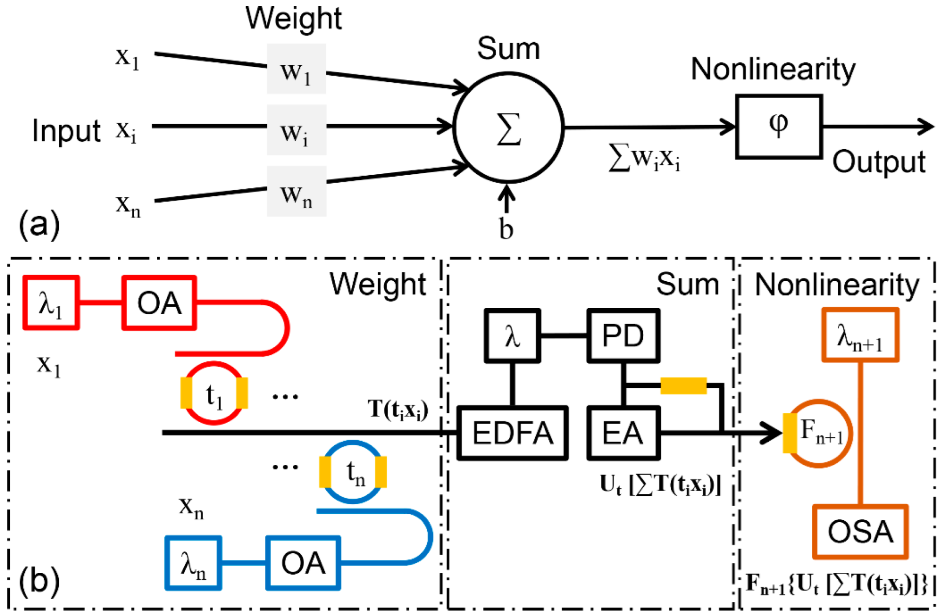
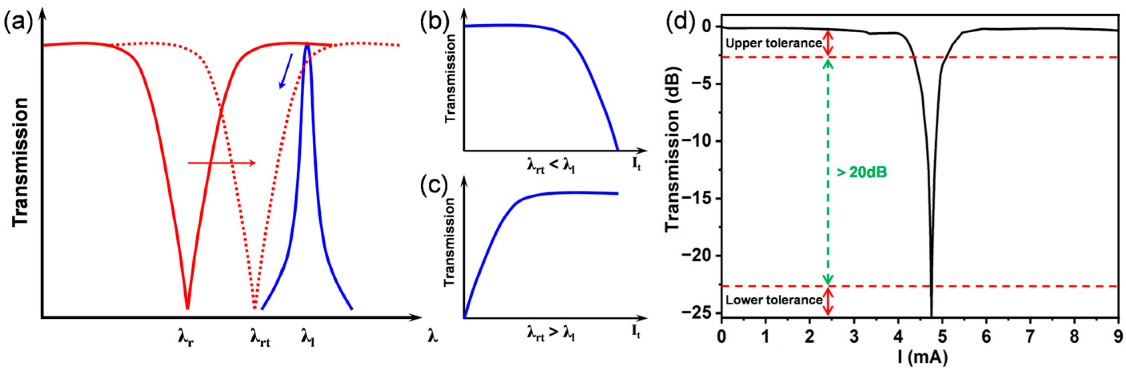
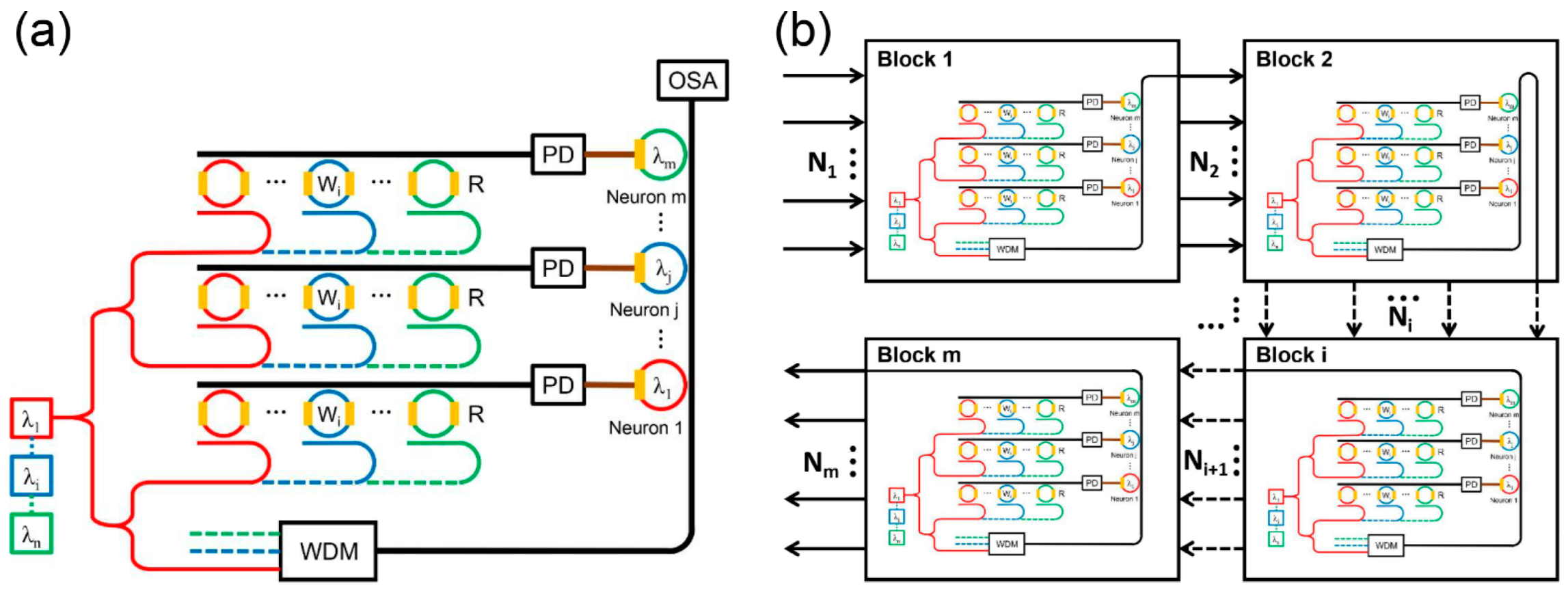
2. Principles and Methods

Biological neurons comprise three primary components: the synapses, soma, and axon [41]. The signal processing of the biological neuron is shown in Figure 1a. Synapses determine the connection strength between neurons where the input signals are weighted. These weighted signals are summed in the soma. Subsequently, the axon applies a nonlinear transformation to the sum. The entire signal processing can be expressed as follows:
y = φ w i · x i + b
where w i is the weight of the ith input signal x i , b is the bias signal of the neuron relating to its current state, and φ is the nonlinear response of the axon, namely the activation function.
The photonic neuron based on thermally tunable MRRs is shown in Figure 1b and mainly includes three functional parts: the weight, sum, and nonlinearity. The input signals x i are from off-chip lasers with different wavelengths and coupled into on-chip cascaded MRRs. The weights of the input signals t i are obtained by thermally tuning a group of cascaded MRRs on-resonance or off-resonance. MRRs are arranged with a WDM framework, which makes all weighted input signals from MRRs collected into one bus waveguide. Then, the weighted input signals T t i · x i are summed into the photocurrent by the PD with an erbium-doped fiber amplifier (EDFA) and a filter. The photocurrent is converted into an excitation voltage U t through a series resistor and further amplified by an electrical amplifier (EA) to enhance voltage gain and drive capability. Finally, the thermally tunable MRR in the nonlinear unit is thermally tuned by the excitation voltage and outputs its nonlinear response. The entire signal processing can be mathematically expressed as follows:
y = F n + 1 { U t   [ i = 1 n T ( t i · x i ) ] }
where t i denotes the transmission ratio of the ith MRR drop port in the weighting unit, x i represents the input signal at the ith wavelength λ i and the above-mentioned bias b from Equation (1) is omitted in the photonic neuron, and F n + 1 serves as the neural activation function and characterizes the nonlinear transfer response of the thermally tunable MRR in the nonlinear unit.

3. Results and Discussion

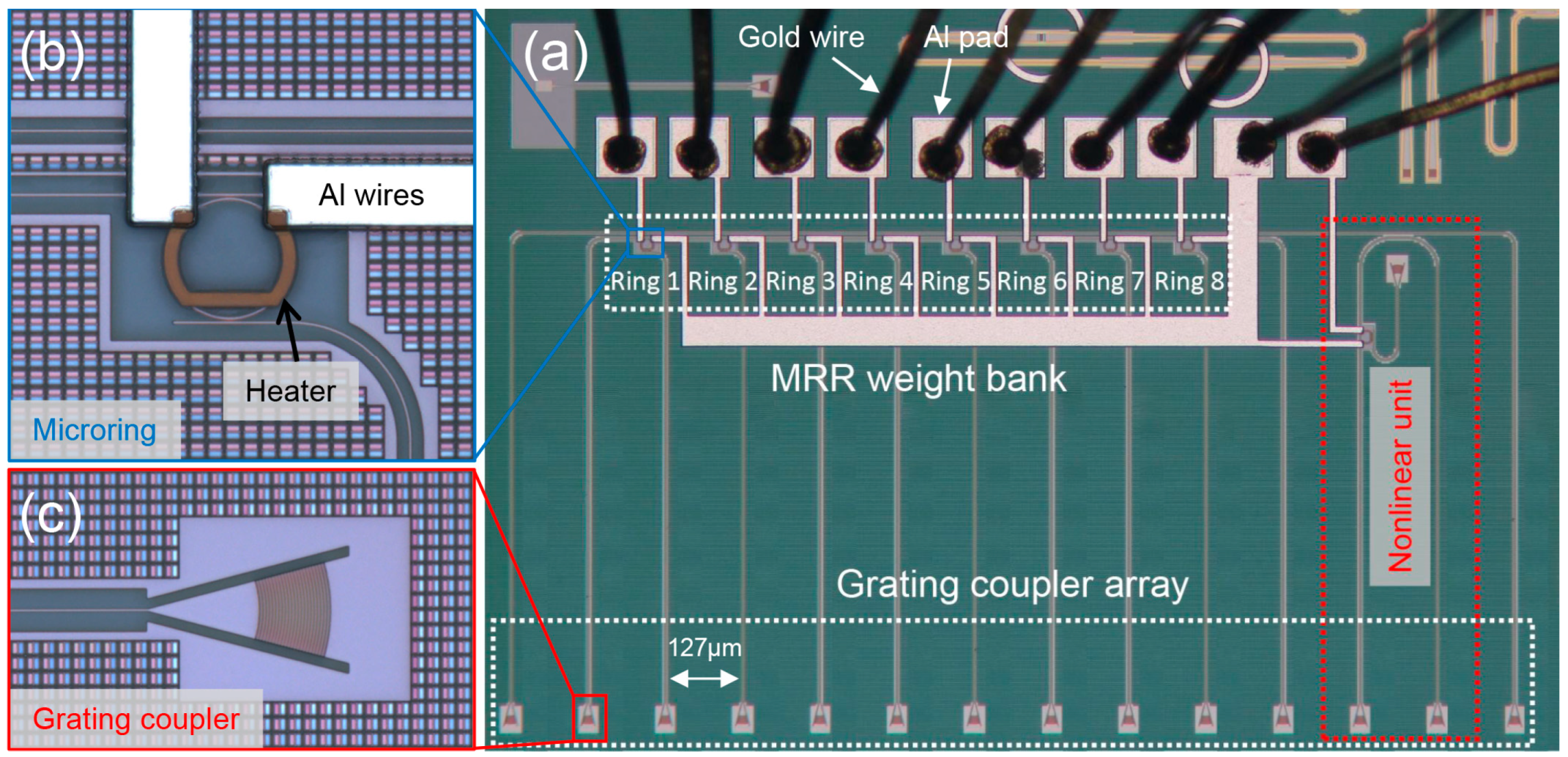
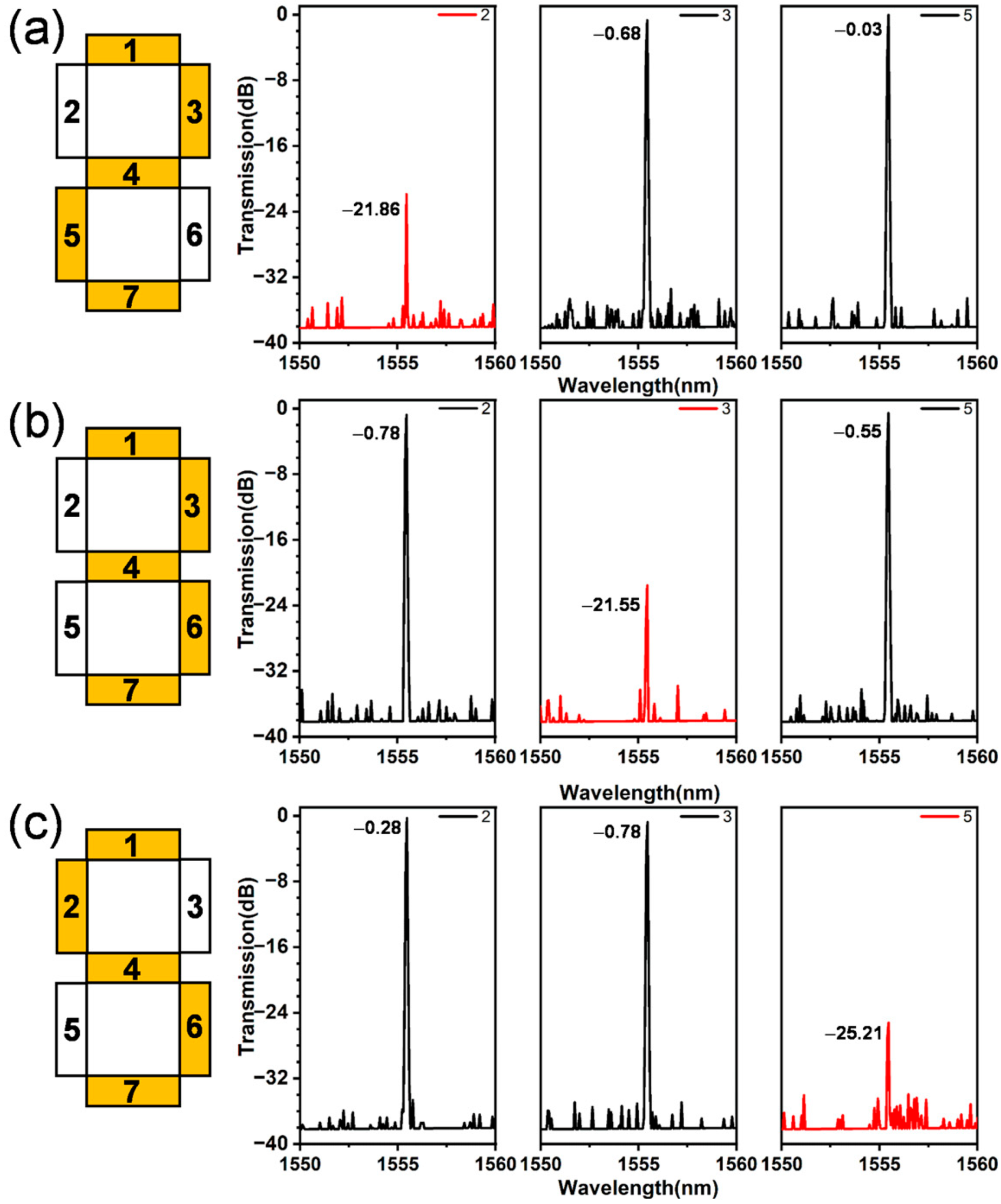
3.1. Device Design and Fabrication

The device was fabricated at CUMEC (http://www.cumec.cn/, accessed on 22 June 2025) using a silicon-on-insulator (SOI) substrate with 2 μm buried oxide (BOX) and a 220 nm top silicon layer. The size of the waveguides was 450 nm × 220 nm. A group of eight MRRs was cascaded via a common drop port waveguide in a WDM architecture. The radius of a single MRR was about 10 μm, with a radius difference of 0.015 μm to offset the resonance wavelengths. The designed FSR and wavelength spacing between each channel was about 9.20 nm and 2.33 nm. A micrograph of the entire device is shown in Figure 2a, including the cascaded MRRs, labeled ring 1 to ring 8; the grating coupler array; and the nonlinear unit. A single MRR with its TiN heater positioned directly above the waveguide arc is detailed in Figure 2b. Each MRR was connected via gold wire bonds to Al pads, as shown in Figure 2a. The grating coupler array was arranged by the space of 127 μm, matching that of the fiber array for multi-wavelength optical input signals. Figure 2c provides a detailed view of the focused grating coupler in the grating coupler array. The MRR in the nonlinear unit marked by a red dashed box is located on the right side of the device.

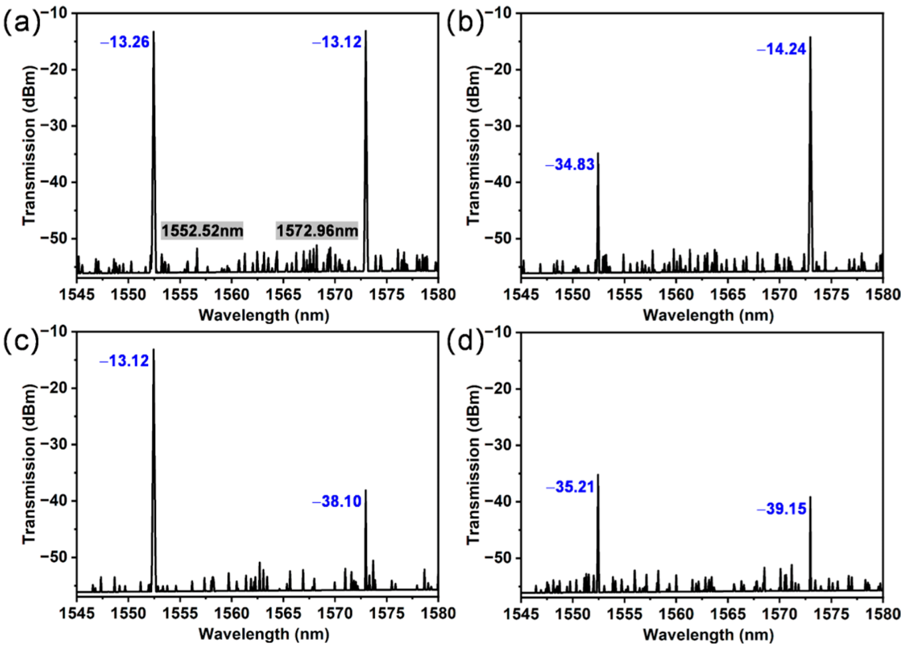
3.2. Matrix Multiplication

To implement the weighting operation, the characteristics of the cascaded MRRs were measured using an amplified spontaneous emission (ASE) broadband source and an OSA. The transmission spectrums of the eight cascaded MRRs measured at the bus waveguide port are shown in Figure 3a. Channel crosstalk was observed between adjacent resonance peaks, particularly between rings 1, 7, and 8; between rings 5 and 4; and between rings 3 and 2. As light propagated sequentially from ring 8 to ring 1, the resonance peaks in the right-side rings dropped earlier into their respective drop ports, leading to notches in the left-side rings’ spectrums. Consequently, in the subsequent experiments, resonance peaks with sufficient spectral separation were employed to avoid extra tuning, leading to more power consumption. Notably, all eight cascaded MRRs could be tuned individually. Figure 3b shows the tuning performance of ring 8 as the tuning voltage applied to its heater increased from 0 to 3.5 V. The original resonance wavelength was 1554.98 nm, with a tuning efficiency of approximately 4.62 mW/nm, obtained from the tuning data. The transmission at the original resonance wavelength, indicated by the gray dotted line, decreased to −25 dB at a tuning voltage of 1.5 V. This corresponds to a weight change from “1” to “0” with an applied voltage of approximately 1.5 V.
For matrix multiplication, the system was designed to perform parallel multiplication of input signals with their corresponding weights without crosstalk. Rings 6 and 8 were selected to apply weights, with their resonance wavelength set at 1552.52 and 1572.96 nm, respectively. Notably, ring 8 was configured in the L-band to avoid confusion. The input signal matrix was set to (1, 1) using two lasers with the same resonance wavelengths matched to the respective MRRs. The computational results are presented in Figure 4. Figure 4a shows the matrix multiplication of the input signal matrix (1, 1) and weight vector (1, 1), which were obtained to make two MRRs on-resonance. Figure 4b shows the matrix multiplication of the input signal matrix (1, 1) and weight vector (0, 1) by applying a voltage of 1 V to make ring 6 off-resonance. The first signal was weighted, and its transmission decreased by 20 dB compared to that of the second signal. Figure 4c shows the matrix multiplication of the input signal matrix (1, 1) and weight vector (1, 0) by making ring 8 off-resonance with a voltage of 1.6 V, yielding a 25 dB suppression of the second signal. Figure 4d shows the matrix multiplication of the input signal matrix (1, 1) and weight vector (0, 0) by applying the voltage of 1.2 V and 1.3 V to rings 6 and 8, respectively, with a total power consumption of approximately 12.78 mW, with almost no thermal crosstalk. These results conclusively demonstrate independent weight configurability through individual thermal tuning of each MRR.

3.3. Recognition Tasks

Based on matrix multiplication, a recognition task was established to characterize the performance of the proposed photonic neuron and neural network. The task involved classifying three distinct digits, 2, 3, and 5, represented using a seven-segment digital tube, as illustrated in Figure 5a. The digits were distinguished by the different values of the four specific digital tubes, B, C, E, and F. Given that the shaded tube was the off-state and its weight was “0,” the input signals of digits 2, 3, and 5 were encoded by four lasers with an on-/off-state. Lasers 1, 2, 3, and 4 correspond to digital tubes B, C, F, and E, respectively. Therefore, for digit 2, lasers 2 and 3 were in the on-state, while lasers 1 and 4 were in the off-state. For digit 3, lasers 3 and 4 were in the on-state, whereas lasers 1 and 4 were in the on-state for digit 5. Then, rings 3, 4, 6, and 8, indicated by arrows in Figure 3a, were used to apply weights to the input signals without channel crosstalk and correspond to the digital tubes B, C, F, and E, respectively. The complete mapping between numerical digits, digital tubes, and rings is systematically presented in Table 1. The weighted signals were summed into the photocurrent by the off-chip PD and transformed into the excitation signals. The neural network adopted a two-layer structure, including four inputs and three outputs, as shown in Figure 5b. The detailed experimental setup for the recognition task is presented in Figure 5c. Lasers 1, 2, 3, and 4 were aligned to the resonance wavelengths of rings, 3, 4, 6, and 8 at 1548.56, 1550.12, 1552.52, and 1554.98 nm, respectively. The responsivity of the PD was approximately 0.9 A/W. The central wavelength of the filter was 1550 nm, with a bandwidth of ±6.5 nm at −3 dB. Digits 2, 3, and 5 were encoded by the off-chip lasers, with different wavelengths serving as input signals. Weights were implemented by using thermally tunable cascaded MRRs 3, 4, 6, and 8, arranged with a WDM framework, which led to all weighted input signals from MRRs being collected in one bus waveguide. The weighted signals were summed into the photocurrent by the off-chip PD and transformed into the excitation signals. The light of laser 5 was coupled to the chip as the input signal for MRR in the nonlinear unit, which was activated by the excitation signals and outputted the results of the nonlinear function.
To achieve the nonlinear function, thermally tunable MRRs were selected for their inherent nonlinear transmission. The schematic of the nonlinear operation is shown in Figure 6a–c. The blue spectrum denotes the laser wavelength λ l , while the red solid and dotted peaks represent the initial and thermally tuned resonance wavelengths of MRR, λ r and λ r t , respectively. As the MRR was thermally tuned, λ r was right-shifted to modulate the amplitude of λ l in the resonance envelope. This mechanism produced two distinct nonlinear response regimes: When λ r t < λ l , the shape of the nonlinear function was the inverse-rectified linear unit (inverse-ReLU), while the shape of the nonlinear function was ReLU when λ r t > λ l , as shown in Figure 6b,c, respectively. Figure 6d shows the nonlinear function of the proposed photonic neuron depicting the relationship between the MRR transmission and excitation current. The resonance wavelength of MRR was 1554.74 nm, while the wavelength of the laser was set to 1555.52 nm. Therefore, the shape of the nonlinear function included two stages, as illustrated in Figure 6b,c. The critical current was about 4.75 mA and the extinction ratio was 25.21 dB. To eliminate the noise caused by spectral jitter, the transmission difference between the high and low values (the upper and lower tolerance) was maintained above 20 dB.
The recognition task was implemented through weighting and nonlinear operations using thermally tunable MRRs. Four lasers were switched between the off and on-states to represent the input signals of numbers 2, 3, and 5. For digit 2, lasers 2 and 3 were in the on-state, while lasers 1 and 4 were in the off-state. For digit 3, lasers 3 and 4 were in the on-state, whereas lasers 1 and 4 were in the on-state for digit 5. To implement the recognition of digit 2, rings 4 and 6 were tuned to be on-resonance, while rings 3 and 8 were tuned to be off-resonance. The result for the recognition of digit 2 is shown in Figure 7a, demonstrating significant transmission contrast between the recognized digits. Specifically, the transmission for digit 2 exhibited an approximately 21 dB attenuation compared to those for digits 3 and 5. The excitation current and power consumption for digit 2 were 4.73 mA and 5.59 mW, while the tunning power was about 8.87 mW. The recognition results of digits 3 and 5 are shown in Figure 7b,c. Digit 3 exhibited an approximately 21 dB lower transmission compared to digits 2 and 5, and digit 5 demonstrated about 25 dB attenuation relative to digits 2 and 3. The excitation current and power consumption for digit 3 were 4.73 mA and 5.59 mW, whereas those for digit 5 were 4.76 mA and 5.65 mW. The tunning powers were about 8.65 mW and 9.38 mW, respectively. As the MRRs depended on the thermal tuning effect, the processing speed of our photonic neural network was relatively limited. Conclusively, digits 2, 3, and 5 were successfully recognized using the photonic neural network based on thermally tunable MRRs. The performance comparison for our work with previous experimental works is shown in Table 2. Although the structure of our proposed neural network was relatively simple and complex recognition tasks with online training were not implemented, ONNs using MRRs for both weighting and nonlinear operations were verified at the system level.

3.4. Multilayer Neural Network

For the recognition task, the neural network consisted of only two layers, including four inputs and three outputs. However, practical applications require more sophisticated multilayer architectures. Figure 8a shows the fundamental neural network unit, which consisted of n inputs and m outputs. All the inputs and outputs and the weight part were in WDM architecture. The weight and nonlinear operations were achieved using thermally tunable MRRs. On the basis of a single neural network, a complex multilayer neural network was established and is presented in Figure 8b, featuring N1 inputs and Nm outputs. Each block included a fundamental neural network representing an individual layer of the multilayer neural network. The numbers of layers and neurons allowed for flexible expansion based on the requirement of different applications. Future research will focus on expanding the network complexity by developing deep photonic neural networks through cascaded MRR-based photonic neurons [33]. An autapse will also be established using the same MRR platform. Additionally, PD and EA in the summation unit will be integrated on a chip to achieve better compactness and miniaturization.
In this paper, on-chip silicon photonic neurons and neural networks were implemented using thermally tunable MRRs for recognition tasks, where the MRRs performed both weighting and nonlinear operations. However, the power efficiency and the speed of the thermally tunable MRRs were not competitive. Neuromorphic photonic chips utilizing MRRs integrated with non-volatile phase change materials (PCMs) for both weighting and nonlinear operations achieved significantly higher power efficiency [22,42], making them a promising replacement for thermal heaters in the future. For the weighting operation, tunning speed can be enhanced by employing MZI-embedded MRRs, which act as resonance switches [43,44]. Regarding the nonlinear operation, reconfigurable phase-relevant devices based on MRRs with graphene–Si heterojunctions enable low-power nonlinear functions [45]. Using reinforcement learning (RL) to optimize ONNs is also a promising direction [46,47]. Furthermore, all neuromorphic processing units can be integrated by hybrid integration to set up an on-chip system, improving computing efficiency, complexity, and scalability [32,48].

4. Conclusions

This study demonstrates an on-chip silicon photonic neural network utilizing thermally tunable MRRs. The weight and nonlinear operations are implemented using on-chip thermally tunable MRRs to implement both weighting and nonlinear operations. The weighting unit employs eight cascaded MRRs in the WDM architecture, leveraging thermal tuning to enable weighted addition with the assistance of PDs. The nonlinear section depends on the MRR nonlinear transmission spectrum, which is analogous to ReLU function. Using the thermally tunable MRR as the nonlinear unit, the matrix multiplication and recognition task of digits 2, 3, and 5 are successfully performed, with about 5.65 mW power consumption for nonlinear operation and a 25 dB extinction ratio between different digit classifications. The CMOS-compatible design fosters scalable implementation of multilayer neural networks. Consequently, there is great potential for the development of highly integrated neuromorphic photonic chips.

Author Contributions

Conceptualization, H.Z., B.H. and Y.X.; methodology, H.Z., B.H. and C.C.; validation, H.Z., B.H. and C.C.; formal analysis, H.Z., B.J. and L.B.; investigation, H.Z. and B.H.; resources, H.Z. and B.H.; data curation, H.Z. and B.H.; writing—original draft preparation, H.Z.; writing—review and editing, B.H., C.C., L.B. and Y.X.; visualization, H.Z.; supervision, B.H. and Y.X.; project administration, H.Z. and B.H.; funding acquisition, H.Z. and B.H. All authors have read and agreed to the published version of the manuscript.

Funding

This work was funded by the National Natural Science Foundation of China, grant numbers 62304014, 62341508, 62204010, 62074011, 62134008, and 62435001; the Beijing Natural Science Foundation, grant number Z220005; the Beijing Outstanding Young Scientist Program, grant number JWZQ20240102009; the Beijing Nova Program, grant number Z201100006820096; the Youth Innovation Promotion Association of the Chinese Academy of Sciences, grant number Y2022045; the China Postdoctoral Science Foundation, grant number 2023M740164; and the Beijing Postdoctoral Research Foundation, grant number 2023-zz-082.

Institutional Review Board Statement

Not applicable.

Informed Consent Statement

Not applicable.

Data Availability Statement

Data are contained within the article.

Conflicts of Interest

The authors declare no conflict of interest.

References

  1. Hashem, I.A.T.; Yaqoob, I.; Anuar, N.B.; Mokhtar, S.; Gani, A.; Khan, S.U. The rise of “big data” on cloud computing: Review and open research issues. Inform. Syst. 2015, 47, 98–115. [Google Scholar] [CrossRef]
  2. Reddy, V.D.; Setz, B.; Rao, G.S.V.R.K.; Gangadharan, G.R.; Aiello, M. Metrics for Sustainable Data Centers. IEEE Trans. Sustain. Comput. 2017, 2, 290–303. [Google Scholar] [CrossRef]
  3. Peng, H.-T.; Nahmias, M.A.; de Lima, T.F.; Tait, A.N.; Shastri, B.J. Neuromorphic Photonic Integrated Circuits. IEEE J. Sel. Top. Quantum Electron. 2018, 24, 1–15. [Google Scholar] [CrossRef]
  4. Lynch, C. How do your data grow? Nature 2008, 455, 28–29. [Google Scholar] [CrossRef]
  5. de Lima, T.F.; Shastri, B.J.; Tait, A.N.; Nahmias, M.A.; Prucnal, P.R. Progress in neuromorphic photonics. Nanophotonics 2017, 6, 577–599. [Google Scholar] [CrossRef]
  6. Merolla, P.A.; Arthur, J.V.; Alvarez-Icaza, R.; Cassidy, A.S.; Sawada, J.; Akopyan, F.; Jackson, B.L.; Imam, N.; Guo, C.; Nakamura, Y.; et al. A million spiking-neuron integrated circuit with a scalable communication network and interface. Science 2014, 345, 668–673. [Google Scholar] [CrossRef]
  7. Benjamin, B.V.; Gao, P.; McQuinn, E.; Choudhary, S.; Chandrasekaran, A.R.; Bussat, J.M.; Alvarez-Icaza, R.; Arthur, J.V.; Merolla, P.A.; Boahen, K. Neurogrid: A Mixed-Analog-Digital Multichip System for Large-Scale Neural Simulations. Proc. IEEE 2014, 102, 699–716. [Google Scholar] [CrossRef]
  8. Schemmel, J.; Brüderle, D.; Grübl, A.; Hock, M.; Meier, K.; Millner, S. A wafer-scale neuromorphic hardware system for large-scale neural modeling. In Proceedings of the 2010 IEEE International Symposium on Circuits and Systems (ISCAS), Paris, France, 30 May–2 June 2010; pp. 1947–1950. [Google Scholar]
  9. Shastri, B.J.; Tait, A.N.; de Lima, T.F.; Pernice, W.H.P.; Bhaskaran, H.; Wright, C.D.; Prucnal, P.R. Photonics for artificial intelligence and neuromorphic computing. Nat. Photon. 2021, 15, 102–114. [Google Scholar] [CrossRef]
  10. Kitayama, K.-I.; Notomi, M.; Naruse, M.; Inoue, K.; Kawakami, S.; Uchida, A. Novel frontier of photonics for data processing—Photonic accelerator. APL Photon. 2019, 4, 090901. [Google Scholar] [CrossRef]
  11. Caulfield, H.J.; Dolev, S. Why future supercomputing requires optics. Nat. Photon. 2010, 4, 261–263. [Google Scholar] [CrossRef]
  12. Kuramochi, E.; Nozaki, K.; Shinya, A.; Takeda, K.; Sato, T.; Matsuo, S.; Taniyama, H.; Sumikura, H.; Notomi, M. Large-scale integration of wavelength-addressable all-optical memories on a photonic crystal chip. Nat. Photon. 2014, 8, 474–481. [Google Scholar] [CrossRef]
  13. Kravtsov, K.; Fok, M.P.; Rosenbluth, D.; Prucnal, P.R. Ultrafast all-optical implementation of a leaky integrate-and-fire neuron. Opt. Express 2011, 19, 2133–2147. [Google Scholar] [CrossRef]
  14. Duport, F.; Schneider, B.; Smerieri, A.; Haelterman, M.; Massar, S. All-optical reservoir computing. Opt. Express 2012, 20, 22783–22795. [Google Scholar] [CrossRef]
  15. Stelzer, F.; Röhm, A.; Vicente, R.; Fischer, I.; Yanchuk, S. Deep neural networks using a single neuron: Folded-in-time architecture using feedback-modulated delay loops. Nat. Commun. 2021, 12, 5164. [Google Scholar] [CrossRef] [PubMed]
  16. Xiang, S.; Ren, Z.; Song, Z.; Zhang, Y.; Guo, X.; Han, G.; Hao, Y. Computing Primitive of Fully VCSEL-Based All-Optical Spiking Neural Network for Supervised Learning and Pattern Classification. IEEE Trans. Neural Netw. Learn. Syst. 2021, 32, 2494–2505. [Google Scholar] [CrossRef]
  17. Fu, T.; Zhang, J.; Sun, R.; Huang, Y.; Xu, W.; Yang, S.; Zhu, Z.; Chen, H. Optical neural networks: Progress and challenges. Light Sci. Appl. 2024, 13, 263. [Google Scholar] [CrossRef]
  18. Fu, F.; Dewang, H.; Ziyang, Z.; Yijie, L.; Shengyao, W.; Zhijuan, G.; Dong-Sheng, L.; Xinhui, D.; Daqian, W.; Xiaowei, L.; et al. Symbiotic evolution of photonics and artificial intelligence: A comprehensive review. Adv. Photon. 2025, 7, 024001. [Google Scholar]
  19. Shen, Y.; Harris, N.C.; Skirlo, S.; Prabhu, M.; Baehr-Jones, T.; Hochberg, M.; Sun, X.; Zhao, S.; Larochelle, H.; Englund, D.; et al. Deep learning with coherent nanophotonic circuits. Nat. Photon. 2017, 11, 441–446. [Google Scholar] [CrossRef]
  20. Zhang, H.; Gu, M.; Jiang, X.D.; Thompson, J.; Cai, H.; Paesani, S.; Santagati, R.; Laing, A.; Zhang, Y.; Yung, M.H.; et al. An optical neural chip for implementing complex-valued neural network. Nat. Commun. 2021, 12, 457. [Google Scholar] [CrossRef]
  21. Pai, S.; Sun, Z.; Hughes, T.W.; Park, T.; Bartlett, B.; Williamson, I.A.D.; Minkov, M.; Milanizadeh, M.; Abebe, N.; Morichetti, F.; et al. Experimentally realized in situ backpropagation for deep learning in photonic neural networks. Science 2023, 380, 398–404. [Google Scholar] [CrossRef]
  22. Feldmann, J.; Youngblood, N.; Wright, C.D.; Bhaskaran, H.; Pernice, W.H.P. All-optical spiking neurosynaptic networks with self-learning capabilities. Nature 2019, 569, 208–214. [Google Scholar] [CrossRef]
  23. Pintus, P.; Dumont, M.; Shah, V.; Murai, T.; Shoji, Y.; Huang, D.; Moody, G.; Bowers, J.E.; Youngblood, N. Integrated non-reciprocal magneto-optics with ultra-high endurance for photonic in-memory computing. Nat. Photon. 2025, 19, 54–62. [Google Scholar] [CrossRef]
  24. Yan, Q.; Ouyang, H.; Tao, Z.; Shen, M.; Du, S.; Zhang, J.; Liu, H.; Hao, H.; Jiang, T. Multi-wavelength optical information processing with deep reinforcement learning. Light Sci. Appl. 2025, 14, 160. [Google Scholar] [CrossRef] [PubMed]
  25. Fu, T.; Zang, Y.; Huang, H.; Du, Z.; Hu, C.; Chen, M.; Yang, S.; Chen, H. On-chip photonic diffractive optical neural network based on a spatial domain electromagnetic propagation model. Opt. Express 2021, 29, 31924–31940. [Google Scholar] [CrossRef] [PubMed]
  26. Luo, X.; Hu, Y.; Ou, X.; Li, X.; Lai, J.; Liu, N.; Cheng, X.; Pan, A.; Duan, H. Metasurface-enabled on-chip multiplexed diffractive neural networks in the visible. Light Sci. Appl. 2022, 11, 158. [Google Scholar] [CrossRef]
  27. Fu, T.; Zang, Y.; Huang, Y.; Du, Z.; Huang, H.; Hu, C.; Chen, M.; Yang, S.; Chen, H. Photonic machine learning with on-chip diffractive optics. Nat. Commun. 2023, 14, 70. [Google Scholar] [CrossRef]
  28. Gu, Z.; Shi, Y.; Zhu, Z.; Li, Z.; Zou, M.; Yang, C.; Liu, Y.; Yu, Y.; Zhang, X. All-integrated multidimensional optical sensing with a photonic neuromorphic processor. Sci. Adv. 2025, 11, eadu7277. [Google Scholar] [CrossRef]
  29. Ashtiani, F.; Geers, A.J.; Aflatouni, F. An on-chip photonic deep neural network for image classification. Nature 2022, 606, 501–506. [Google Scholar] [CrossRef]
  30. Dong, B.; Aggarwal, S.; Zhou, W.; Ali, U.E.; Farmakidis, N.; Lee, J.S.; He, Y.; Li, X.; Kwong, D.-L.; Wright, C.D.; et al. Higher-dimensional processing using a photonic tensor core with continuous-time data. Nat. Photon. 2023, 17, 1080–1088. [Google Scholar] [CrossRef]
  31. Ohno, S.; Tang, R.; Toprasertpong, K.; Takagi, S.; Takenaka, M. Si Microring Resonator Crossbar Array for On-Chip Inference and Training of the Optical Neural Network. ACS Photon. 2022, 9, 2614–2622. [Google Scholar] [CrossRef]
  32. Bai, B.; Yang, Q.; Shu, H.; Chang, L.; Yang, F.; Shen, B.; Tao, Z.; Wang, J.; Xu, S.; Xie, W.; et al. Microcomb-based integrated photonic processing unit. Nat. Commun. 2023, 14, 66. [Google Scholar] [CrossRef] [PubMed]
  33. Huang, Y.; Jiang, Z.; Gu, J.; Yuan, G.; Zheng, Y.; Li, K.; Chen, M.K.; Wang, L.; Geng, Z. Cascaded Micro-Ring Resonators for Low-Crosstalk High-Density Photonic Convolutional Computing. Laser Photon. Rev. 2025, 2401874. [Google Scholar] [CrossRef]
  34. Bandyopadhyay, S.; Sludds, A.; Krastanov, S.; Hamerly, R.; Harris, N.; Bunandar, D.; Streshinsky, M.; Hochberg, M.; Englund, D. Single-chip photonic deep neural network with forward-only training. Nat. Photon. 2024, 18, 1335–1343. [Google Scholar] [CrossRef]
  35. Huang, C.; Fujisawa, S.; de Lima, T.F.; Tait, A.N.; Blow, E.C.; Tian, Y.; Bilodeau, S.; Jha, A.; Yaman, F.; Peng, H.-T.; et al. A silicon photonic–electronic neural network for fibre nonlinearity compensation. Nat. Electron. 2021, 4, 837–844. [Google Scholar] [CrossRef]
  36. Cheng, J.; Xie, Y.; Liu, Y.; Song, J.; Liu, X.; He, Z.; Zhang, W.; Han, X.; Zhou, H.; Zhou, K.; et al. Human emotion recognition with a microcomb-enabled integrated optical neural network. Nanophotonics 2023, 12, 3883–3894. [Google Scholar] [CrossRef]
  37. Zhang, W.; Huang, C.; Peng, H.-T.; Bilodeau, S.; Jha, A.; Blow, E.; de Lima, T.F.; Shastri, B.J.; Prucnal, P. Silicon microring synapses enable photonic deep learning beyond 9-bit precision. Optica 2022, 9, 579–584. [Google Scholar] [CrossRef]
  38. Xiang, J.; Torchy, A.; Guo, X.; Su, Y. All-Optical Spiking Neuron Based on Passive Microresonator. J. Light. Technol. 2020, 38, 4019–4029. [Google Scholar] [CrossRef]
  39. Xiang, J.; Zhang, Y.; Zhao, Y.; Guo, X.; Su, Y. All-optical silicon microring spiking neuron. Photon. Res. 2022, 10, 939–946. [Google Scholar] [CrossRef]
  40. Yu, W.; Zheng, S.; Zhao, Z.; Wang, B.; Zhang, W. Reconfigurable Low-Threshold All-Optical Nonlinear Activation Functions Based on an Add-Drop Silicon Microring Resonator. IEEE Photon. J. 2022, 14, 5559807. [Google Scholar] [CrossRef]
  41. Nahmias, M.A.; Shastri, B.J.; Tait, A.N.; Prucnal, P.R. A Leaky Integrate-and-Fire Laser Neuron for Ultrafast Cognitive Computing. IEEE J. Sel. Top. Quant. 2013, 19, 1800212. [Google Scholar] [CrossRef]
  42. Li, T.; Li, Y.; Wang, Y.; Liu, Y.; Liu, Y.; Wang, Z.; Miao, R.; Han, D.; Hui, Z.; Li, W. Neuromorphic Photonics Based on Phase Change Materials. Nanomaterials 2023, 13, 1756. [Google Scholar] [CrossRef] [PubMed]
  43. Chen, B.; Qi, Y.; Dai, T.; Guo, X.; Wang, Y.; Zhang, Q.; Yu, H.; Yang, J. Hitless Wavelength-Selective Switch Using a Single Microring Resonator Assisted With a Symmetric MZI. IEEE Photon. Technol. Lett. 2020, 32, 402–405. [Google Scholar] [CrossRef]
  44. Chen, B.; Zhang, Z.; Ye, L.; Dai, T.; Yu, H.; Wang, Y.; Yang, J. Silicon-Based MZI-Embedded Microring Array With Hitless and FSR-Alignment-Free Wavelength Selection. IEEE Photon. Technol. Lett. 2022, 34, 436–439. [Google Scholar] [CrossRef]
  45. Zhong, C.; Liao, K.; Dai, T.; Wei, M.; Ma, H.; Wu, J.; Zhang, Z.; Ye, Y.; Luo, Y.; Chen, Z.; et al. Graphene/silicon heterojunction for reconfigurable phase-relevant activation function in coherent optical neural networks. Nat. Commun. 2023, 14, 6939. [Google Scholar] [CrossRef]
  46. Tang, Y.; Zamani, P.T.; Chen, R.; Ma, J.; Qi, M.; Yu, C.; Gao, W. Device-System End-to-End Design of Photonic Neuromorphic Processor Using Reinforcement Learning. Laser Photon. Rev. 2022, 17, 2200381. [Google Scholar] [CrossRef]
  47. Bueno, J.; Maktoobi, S.; Froehly, L.; Fischer, I.; Jacquot, M.; Larger, L.; Brunner, D. Reinforcement learning in a large-scale photonic recurrent neural network. Optica 2018, 5, 756–760. [Google Scholar] [CrossRef]
  48. Atabaki, A.H.; Moazeni, S.; Pavanello, F.; Gevorgyan, H.; Notaros, J.; Alloatti, L.; Wade, M.T.; Sun, C.; Kruger, S.A.; Meng, H.; et al. Integrating photonics with silicon nanoelectronics for the next generation of systems on a chip. Nature 2018, 556, 349–354. [Google Scholar] [CrossRef]
Figure 1. (a) Schematic diagram of signal processing in a biological neuron. (b) Architecture of the photonic neuron implemented using thermally tunable MRRs. The orange blocks represent thermally tuned resistors and series resistor in the weighting, nonlinear, and sum units, respectively. λ refers to the 1550 nm filter with the bandwidth of ±6.5 nm at −3 dB in the sum unit. The laser wavelength λ n + 1 is precisely aligned with the resonance wavelength of the MRR in the nonlinearity unit. OA, optical attenuator; OSA, optical spectrum analyzer.
Photonics 12 00640 g001
Figure 2. (a) Micrograph of the entire device, consisting of cascaded MRRs, a grating coupler array, and a nonlinear unit. (b) The micrograph of the single MRR with its TiN heater. (c) A detailed view of the grating coupler in the grating coupler array.
Photonics 12 00640 g002
Figure 3. (a) Transmission spectrums of eight cascaded MRRs. (b) Tuning performance of ring 8, with tuning voltage ranging from 0 to 3.5 V in 0.5 V increments.
Photonics 12 00640 g003
Figure 4. Results of the matrix multiplication of the weight operation of input signal matrix (1, 1) and weight vectors (a) (1, 1), (b) (0, 1), (c) (1, 0), and (d) (0, 0) obtained by thermally tuning MRRs.
Photonics 12 00640 g004
Figure 5. (a) Digits 2, 3, and 5, represented by the seven-segment digital tube. (b) The structure of the neural network, with four inputs and three outputs. (c) The experimental setup for the recognition task. PM, picoammeter.
Photonics 12 00640 g005
Figure 6. (a) Schematic of the nonlinear operation. (b) The shape of the nonlinear function when λ r t < λ l . (c) The shape of the nonlinear function when λ r t > λ l . (d) The nonlinear function of the proposed photonic neuron based on the thermally tunable MRR.
Photonics 12 00640 g006
Figure 7. Results for the recognition task of digits 2, 3, and 5. (a) Result for the recognition of digit 2; (b) Result for the recognition of digit 3; (c) Result for the recognition of digit 5.
Photonics 12 00640 g007
Figure 8. (a) Architecture of the fundamental neural network with n inputs and m outputs. (b) Architecture of a complex multilayer neural network with N1 inputs and Nm outputs.
Photonics 12 00640 g008
Table 1. The corresponding relationships between digits, digital tubes, and rings.
DigitTube BTube CTube ETube FRing 3Ring 4Ring 6Ring 8
201010110
300110011
510101001
Table 2. Performance comparison for our work with previous experimental works.
RefStructureMRRs’ FunctionsSizeComputing Performance
WeightNonlinearityOthers
[31]MRR array--4 × 415 TOPS/W
[32]Microcomb +MRRs-Source1 × 41.04 TOPS/mm
[29]Attenuator +MRR modulator--1 × 4570 ps
[34]MZI + MRR modulator--1 × 610 fJ/OP
This workThermally tunable MRRs-1 × 410.41 mW
Disclaimer/Publisher’s Note: The statements, opinions and data contained in all publications are solely those of the individual author(s) and contributor(s) and not of MDPI and/or the editor(s). MDPI and/or the editor(s) disclaim responsibility for any injury to people or property resulting from any ideas, methods, instructions or products referred to in the content.

