Polarization-Insensitive Silicon Photonic Variable Optical Attenuator


Abstract
1. Introduction
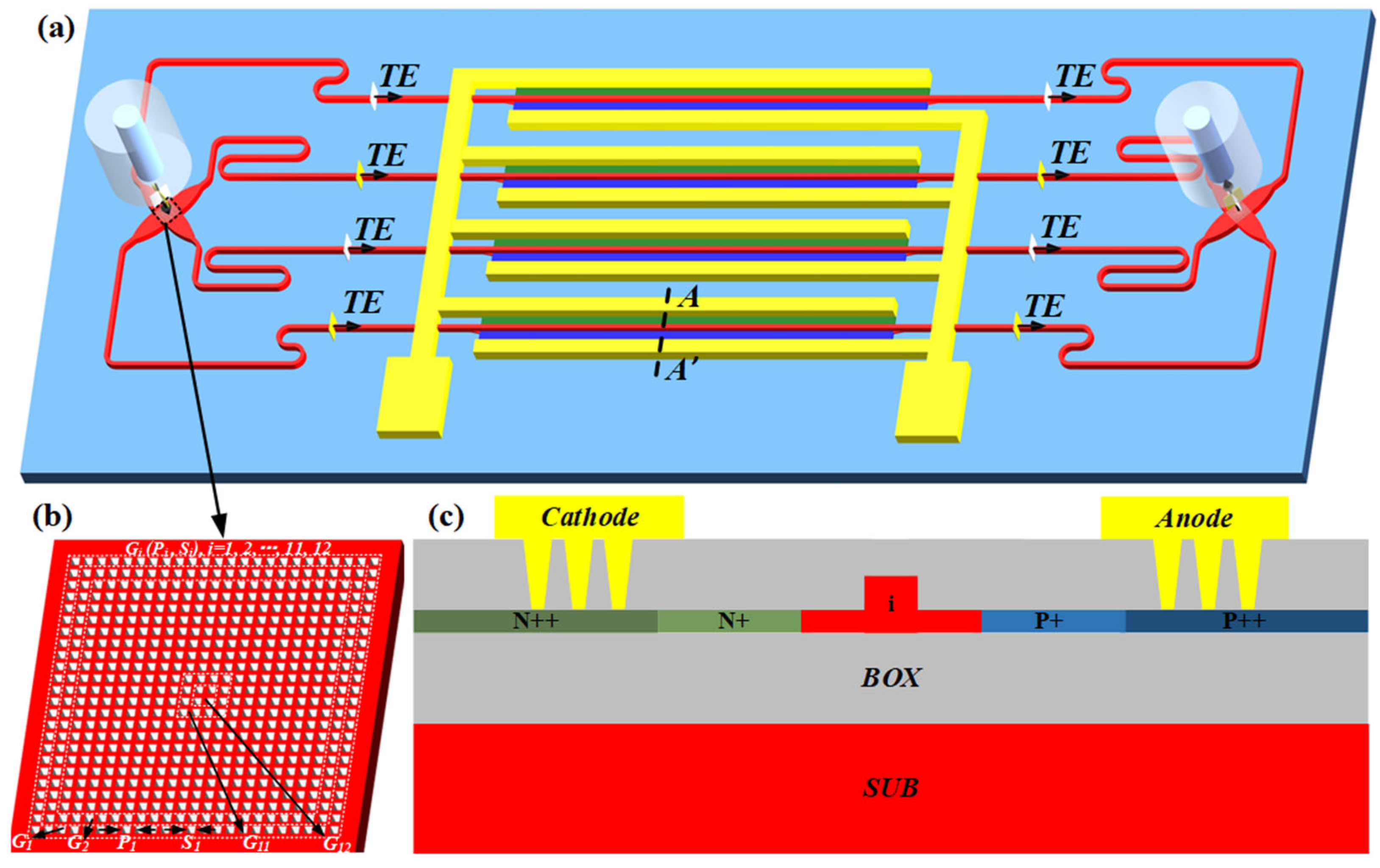
2. Device Design
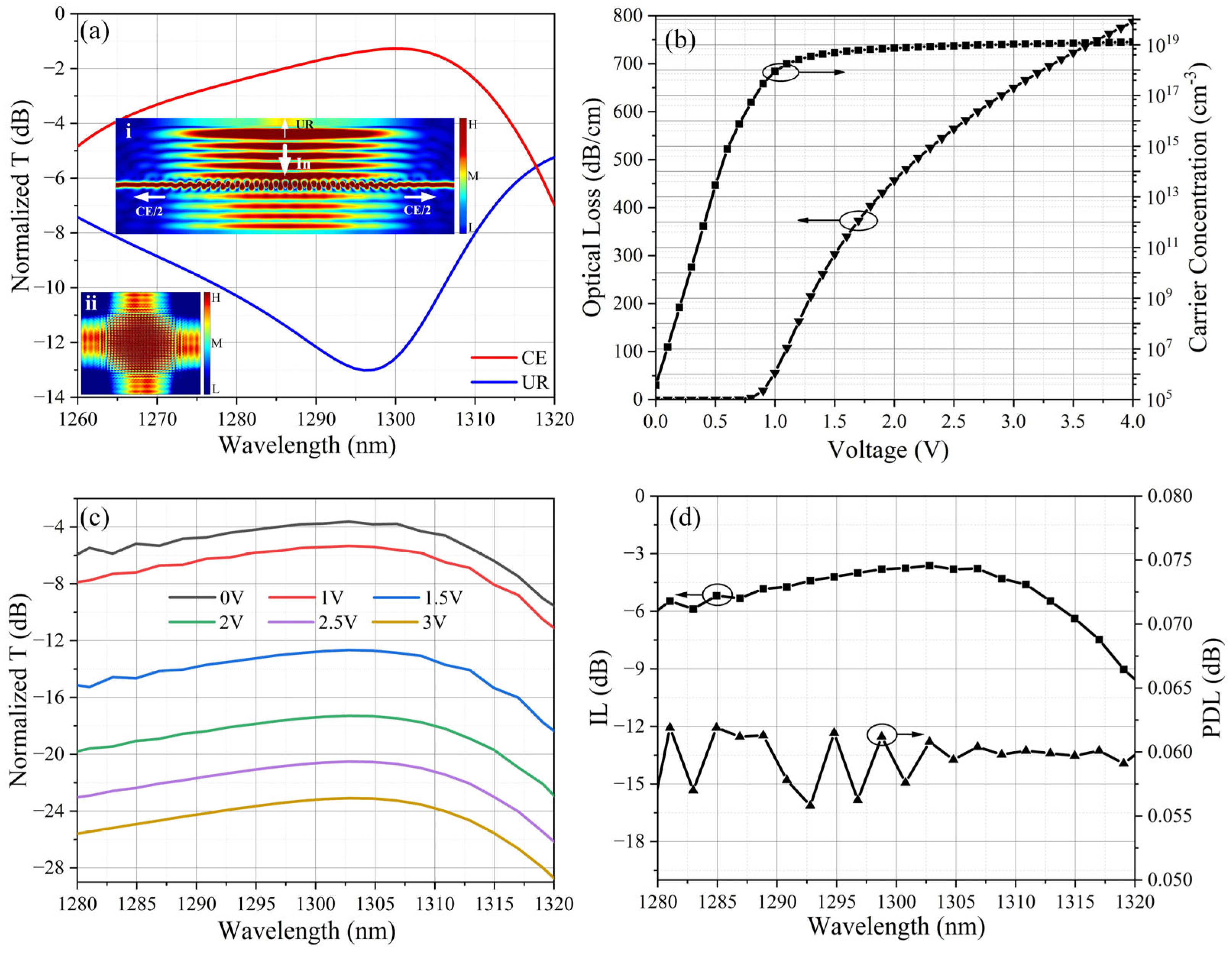
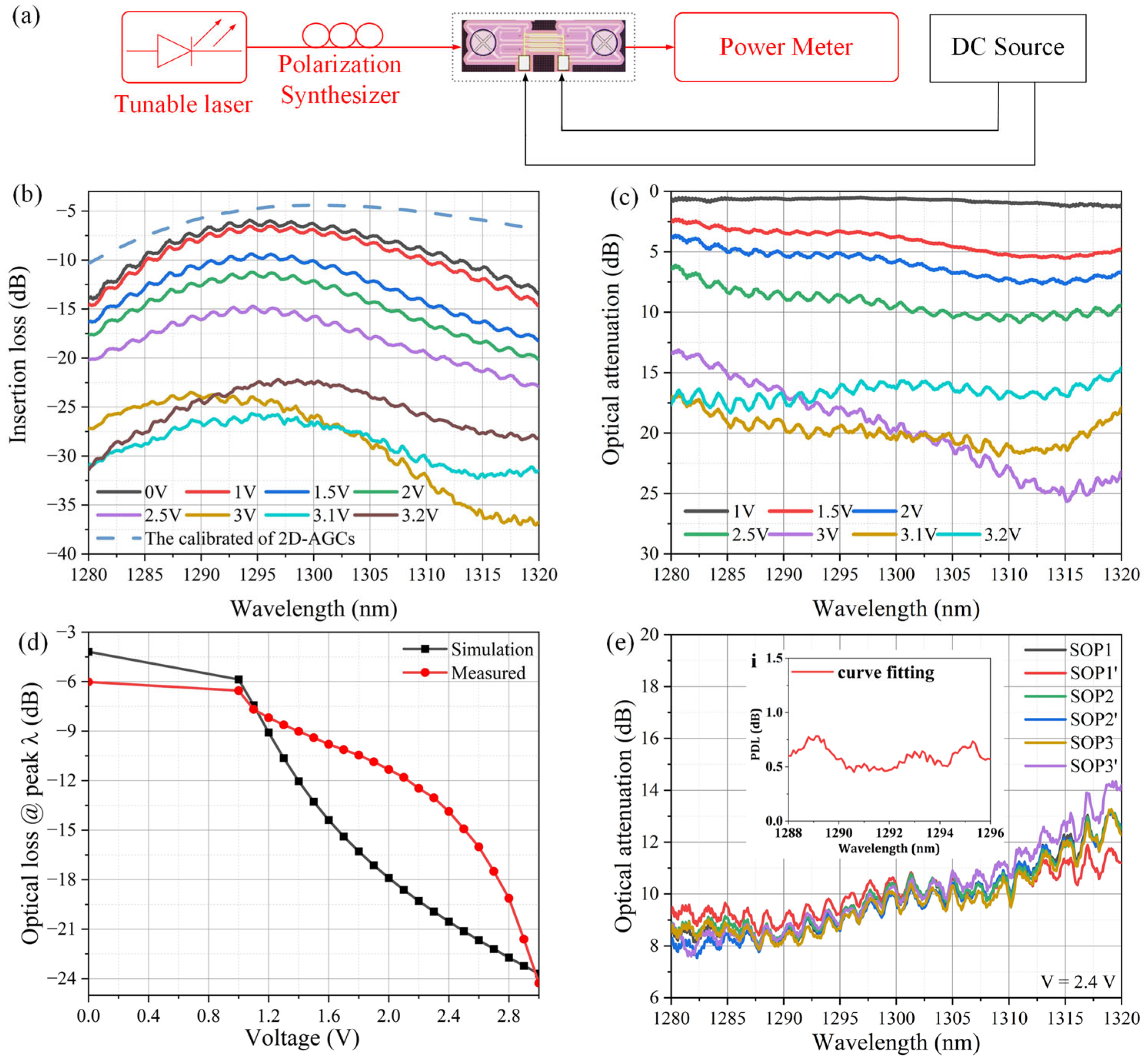
3. Results and Discussion
4. Conclusions
Author Contributions
Funding
Institutional Review Board Statement
Informed Consent Statement
Data Availability Statement
Conflicts of Interest
References
- Khonina, S.N.; Kazanskiy, N.L.; Butt, M.A.; Karpeev, S.V. Optical multiplexing techniques and their marriage for on-chip and optical fiber communication: A review. Opto-Electron. Adv. 2022, 5, 210127. [Google Scholar] [CrossRef]
- Veeranna, D.G.; Nagabushanam, M.; Boraiah, S.S.; Muniyappa, R.; Narayanappa, D.S. Fiber Optic Communication: Evolution, Technology, Recent Developments, and Future Trends. In Modeling and Optimization of Optical Communication Networks; John Wiley & Sons: Hoboken, NJ, USA, 2023; pp. 163–177. [Google Scholar]
- Liu, Q.H.; Pan, P.; You, J.; Zhang, J.S.; Wang, Y.; Wang, Y.T.; Wang, L.L.; An, J.M.; Cui, D.J.; Zhou, L. Four-stage cascaded variable optical attenuator with large attenuation range for quantum key distribution. Chin. Phys. B 2023, 32, 054207. [Google Scholar] [CrossRef]
- Ni, F.C.; Xie, Z.T.; Ma, Q.C.; Tao, J.; Wu, L.; Yu, C.Y.; Huang, X.G. Variable optical attenuator and modulator based on a graphene plasmonic gap waveguide. Opt. Commun. 2018, 426, 251–256. [Google Scholar] [CrossRef]
- Hah, D. Linear variable optical attenuators with shaped-finger comb-drive actuators. Appl. Opt. 2020, 59, 277–284. [Google Scholar] [CrossRef] [PubMed]
- Wan, J.; Xue, F.L.; Liu, C.J.; Huang, S.Q.; Fan, S.Z.; Hu, F.R. Optofluidic variable optical attenuator controlled by electricity. Appl. Opt. 2018, 57, 8114–8118. [Google Scholar] [CrossRef] [PubMed]
- Nishi, H.; Tsuchizawa, T.; Watanabe, T.; Shinojima, H.; Park, S.; Kou, R.; Yamada, K.; Itabashi, S. Monolithic integration of a silica-based arrayed waveguide grating filter and silicon variable optical attenuators based on p–i–n carrier-injection structure. Appl. Phys. Express 2010, 3, 102203. [Google Scholar] [CrossRef]
- Lagosh, A.; Guldimann, B.; Huszka, G.; Sattari, H.; Ahlers, B.; Kerr, G.; Melozzi, M.; Rahnama, P.; Nishizawa, T.; Quack, N. MEMS shutter based variable optical attenuator integrated with large core multimode rectangular waveguides. In Proceedings of the IEEE/LEOS International Conference on Optical MEMS, Gainesville, FL, USA, 25–29 January 2021. [Google Scholar]
- Sun, S.J.; Lian, T.H.; Sun, X.Q.; Zhu, M.; Che, Y.H.; Wang, X.B.; Zhang, D.M. Dual-Mode Variable Optical Attenuator Based on Polymer Waveguide Mach–Zehnder Interferometer. IEEE Photonics Technol. Lett. 2023, 35, 442–445. [Google Scholar] [CrossRef]
- Wei, M.L.; Ma, H.; Sun, C.L.; Zhong, C.Y.; Ye, Y.T.; Zhang, P.; Liu, R.N.; Li, J.Y.; Li, L.; Tang, B.; et al. TDFA-band silicon optical variable attenuator. Prog. Electromagn. Res. 2022, 174, 33–42. [Google Scholar] [CrossRef]
- Nedeljkovic, M.; Littlejohns, C.G.; Khokhar, A.Z.; Banakar, M.; Cao, W.; Penades, J.S.; Tran, D.T.; Gardes, F.Y.; Thomson, D.J.; Reed, G.T.; et al. Silicon-on-insulator free-carrier injection modulators for the mid-infrared. Opt. Lett. 2019, 44, 915–918. [Google Scholar] [CrossRef]
- Yuan, P.; Wang, Y.; Wu, Y.D.; An, J.M.; Hu, X.W. Design and fabrication of two kind of SOI-based EA-type VOAs. Opt. Laser Technol. 2018, 102, 166–173. [Google Scholar] [CrossRef]
- Sahin, U.; Bor, E.; Kurt, H.; Turduev, M. Genetically optimized design of ultra-compact and highly efficient waveguide crossing, optical attenuator and reflector. In Proceedings of the 21st International Conference on Transparent Optical Networks (ICTON), Angers, France, 9–13 July 2019. [Google Scholar]
- Chen, S.T.; Shi, Y.C.; He, S.L.; Dai, D.X. Variable optical attenuator based on a reflective Mach–Zehnder interferometer. Opt. Commun. 2016, 361, 55–58. [Google Scholar] [CrossRef]
- Ma, J.C.; Wang, L.L.; Zhang, J.S.; Wang, Y.; Chen, J.; Sun, B.L.; Zhou, T.H.; Cui, P.W.; Wu, Y.D.; An, J.M. Compactly integrated polarization insensitive 24-channel variable optical attenuator arrays using silica-based. Opt. Commun. 2023, 549, 129932. [Google Scholar] [CrossRef]
- Blasl, M.; Bornhorst, K.; Costache, F. Polarization insensitive variable optical attenuator based on field induced waveguides with a liquid crystal core. In Proceedings of the Optical Fiber Communication Conference, Los Angeles, CA, USA, 22–26 March 2015. [Google Scholar]
- Nishi, H.; Tsuchizawa, T.; Shinojima, H.; Watanabe, T.; Itabashi, S.; Kou, R.; Fukuda, H.; Yamada, K. Low-polarization-dependent silica waveguide monolithically integrated on SOI photonic platform. J. Light. Technol. 2013, 31, 1821–1827. [Google Scholar] [CrossRef]
- Li, A.; Zhao, N.Y.; Liu, C.Y.; Lu, R.T.; Wang, R.X.; Qiu, C.; Wu, A.M. Algorithmically calibrated optical switch with high-extinction-ratio and low-polarization-dependence on 3-μm-thick SOI platform. Opt. Commun. 2024, 560, 130447. [Google Scholar] [CrossRef]
- Zou, J.H.; Yu, Y.; Zhang, X.L. Two-dimensional grating coupler with a low polarization dependent loss of 0.25 dB covering the C-band. Opt. Lett. 2016, 41, 4206–4209. [Google Scholar] [CrossRef]
- Xue, Y.Y.; Chen, H.; Bao, Y.J.; Dong, J.J.; Zhang, X.L. Two-dimensional silicon photonic grating coupler with low polarization-dependent loss and high tolerance. Opt. Express 2019, 27, 22268–22274. [Google Scholar] [CrossRef] [PubMed]
- Zhang, Z.Y.; Zhang, K.X.; Cheng, Q.; Li, M.X.; Liu, T.J.; Huang, B.J.; Zhang, Z.; Liu, H.W.; Li, H.Q.; Niu, P.J.; et al. High-Efficiency Two-Dimensional Perfectly Vertical Grating Coupler with Ultra-Low Polarization Dependent Loss and Large Fibre Misalignment Tolerance. IEEE J. Quantum Electron. 2021, 57, 5. [Google Scholar] [CrossRef]
- Zhang, Z.Y.; Chen, X.; Cheng, Q.; Ali, Z.K.; Zhang, Z.; Yan, X.Z.; Huang, B.J.; Chen, H.D.; Liu, H.W.; Li, H.Q.; et al. Two-dimensional apodized grating coupler for polarization-independent and surface-normal optical coupling. J. Light. Technol. 2020, 38, 4037–4044. [Google Scholar] [CrossRef]
- Zhang, Z.Y.; Huang, B.J.; Wang, Q.X.; Chen, Z.L.; Li, K.; Zhang, K.X.; Li, M.X.; Jiang, H.; Xing, J.M.; Liu, T.J.; et al. Polarization-insensitive silicon intensity modulator with a maximum speed of 224 Gb/s. Photonics Res. 2025, 13, 274. [Google Scholar] [CrossRef]
- Yang, K.Y.; Shirpurkar, C.; White, A.D.; Zang, J.Z.; Chang, L.; Ashtiani, F.; Guidry, M.A.; Lukin, D.M.; Pericherla, S.V.; Yang, J.; et al. Multi-dimensional data transmission using inverse-designed silicon photonics and microcombs. Nat. Commun. 2022, 13, 7862. [Google Scholar] [CrossRef]
- Zhang, Z.Y.; Meng, C.R.; Jiang, H.; Li, M.X.; Lv, X.Q.; Zhang, K.X.; Liu, T.J.; Wang, Q.X.; Huang, B.J. Ultra-compact and low-loss silicon nitride optical mode-size converter. Opt. Eng. 2024, 63, 105106. [Google Scholar] [CrossRef]
- Uddin, M.R.; Wallner, J.; Dikshit, A.; Timalsina, Y.; Khatijah, S.; Fahrenkopf, N.M.; Harame, D.L. Silicon rib-waveguide based on-chip optical attenuator. In Proceedings of the Optica Advanced Photonics Congress, Maastricht, Limburg, The Netherlands, 24–28 July 2022. [Google Scholar]
- Sun, H.Q.B.; Zhou, W.; Zhang, Z.J.; Wan, Z.J. A MEMS variable optical attenuator with ultra-low wavelength-dependent loss and polari-zation-dependent loss. Micromachines 2018, 9, 632. [Google Scholar] [CrossRef] [PubMed]
- Wu, Q.Q.; Zhou, L.J.; Sun, X.M.; Zhu, H.K.; Lu, L.J.; Chen, J.P. Silicon thermo-optic variable optical attenuators based on Mach–Zehnder interference structures. Opt. Commun. 2015, 341, 69–73. [Google Scholar] [CrossRef]
- Nicolescu, E.; Mao, C.C.; Fardad, A.; Escuti, M. Polarization-insensitive variable optical attenuator and wavelength blocker using liquid crystal polarization gratings. J. Light. Technol. 2010, 28, 3121–3127. [Google Scholar] [CrossRef]
- Yuan, P.; Wang, Y.; Wu, Y.D.; An, J.M. Variable optical attenuators based on SOI with 3 μm top silicon layer. Appl. Opt. 2019, 58, 4630–4636. [Google Scholar] [CrossRef]
- Kurudi, S.; Das, B.K. Design and Demonstration of Polarization Independent Variable Optical Attenuator with SOI Wave-guides. In Proceedings of the 13th International Conference on Fiber Optics and Photonics, Kanpur, India, 4–8 December 2016. [Google Scholar]
- Huang, Y.M.; Lu, L.D.; Chen, G.; Xu, Y.J.; Zhu, L.Q. Design and optimization of an SOI-based electro-absorption-type VOA. Appl. Opt. 2023, 62, 6316–6322. [Google Scholar] [CrossRef]


| Parameters | G1–G6 | G7 | G8 | G9 | G10 | G11 | G12 |
|---|---|---|---|---|---|---|---|
| Pitch P (nm) | 450 | 460 | 460 | 450 | 450 | 440 | 440 |
| Hole span S (nm) | 270 | 280 | 273 | 265 | 256 | 250 | 240 |
| Ref. | Type | Length (μm) | Attenuation (dB) | PDL (dB) | Driving Conditions |
|---|---|---|---|---|---|
| [14] | Si-TO | 125 | 35.5 | - | 10.8 mW |
| [15] | SiO2-TO | 1.5 × 10⁴ | 43 | 0.7 a | 200 mW |
| [26] | Si-EO | 30 | 2.6 | - | 1.5 V |
| [27] | MEMS | - | 20 | 0.15 a | - |
| [28] | Si-TO | 50 | 30 | - | 50 mW |
| [29] | LCPGs | - | 50 | 0.3 a | 20 V |
| [30] | Si-EO | 1 × 10⁴ | 20 | - | 470 mW |
| [31] | Si-EO | 5000 | 4 | 0.2 b | 50 mA |
| [32] | Si-EO | 1380 | 60.11/59.08 | - | 33 V/3.2 V |
| This work | Si-EO | 150 | 18 | 0.5 a | 3 V |
Disclaimer/Publisher’s Note: The statements, opinions and data contained in all publications are solely those of the individual author(s) and contributor(s) and not of MDPI and/or the editor(s). MDPI and/or the editor(s) disclaim responsibility for any injury to people or property resulting from any ideas, methods, instructions or products referred to in the content. |
© 2025 by the authors. Licensee MDPI, Basel, Switzerland. This article is an open access article distributed under the terms and conditions of the Creative Commons Attribution (CC BY) license (https://creativecommons.org/licenses/by/4.0/).
Share and Cite
Li, M.; Zhang, Y.; Jiang, H.; Wang, H.; Luo, D.; Yang, J.; Li, Y.; Zhang, Z. Polarization-Insensitive Silicon Photonic Variable Optical Attenuator. Photonics 2025, 12, 549. https://doi.org/10.3390/photonics12060549
Li M, Zhang Y, Jiang H, Wang H, Luo D, Yang J, Li Y, Zhang Z. Polarization-Insensitive Silicon Photonic Variable Optical Attenuator. Photonics. 2025; 12(6):549. https://doi.org/10.3390/photonics12060549
Chicago/Turabian StyleLi, Meixin, Yuxuan Zhang, Hao Jiang, Haoran Wang, Danni Luo, Jing Yang, Yabin Li, and Zanyun Zhang. 2025. "Polarization-Insensitive Silicon Photonic Variable Optical Attenuator" Photonics 12, no. 6: 549. https://doi.org/10.3390/photonics12060549
APA StyleLi, M., Zhang, Y., Jiang, H., Wang, H., Luo, D., Yang, J., Li, Y., & Zhang, Z. (2025). Polarization-Insensitive Silicon Photonic Variable Optical Attenuator. Photonics, 12(6), 549. https://doi.org/10.3390/photonics12060549