Design and Optimization of Optical NAND and NOR Gates Using Photonic Crystals and the ML-FOLD Algorithm


Abstract
1. Introduction
- Simplified Process: Avoids hyperparameter tuning and iterative learning.
- Efficiency: Uses basic arithmetic, outperforming iterative genetic algorithms.
2. Proposed Configuration for Realizing Optical NAND and NOR Gates
3. Methods
3.1. Introduction to ML-FOLD Optimization
3.2. ML-FOLD Formula and Rationale
- : Output power when input A is active and B is inactive.
- Output power when input A is inactive and B is active.
- : Output power when both inputs A and B are active.
- : Output power when both inputs A and B are inactive.
- NOR Gate: A high output (logical “1”) is required only when both inputs are off (A = 0, B = 0), with low outputs (logical “0”) for all other states. A high value thus indicates a large preds_AB_0 relative to the product of the other outputs, favoring configurations where the (0,0) state is distinctly prominent.
- NAND Gate: A low output (logical “0”) is expected only when both inputs are active (A = 1, B = 1), with high outputs (logical “1”) elsewhere. Here, a high reflects a small preds_AB_1 relative to the product of the other outputs, highlighting configurations that effectively suppress the (1,1) state.
3.3. Implementation of ML-FOLD
- Data Preprocessing: The dataset is loaded into a Pandas DataFrame.
- Metric Calculation: The value is computed for each configuration using the formula above.
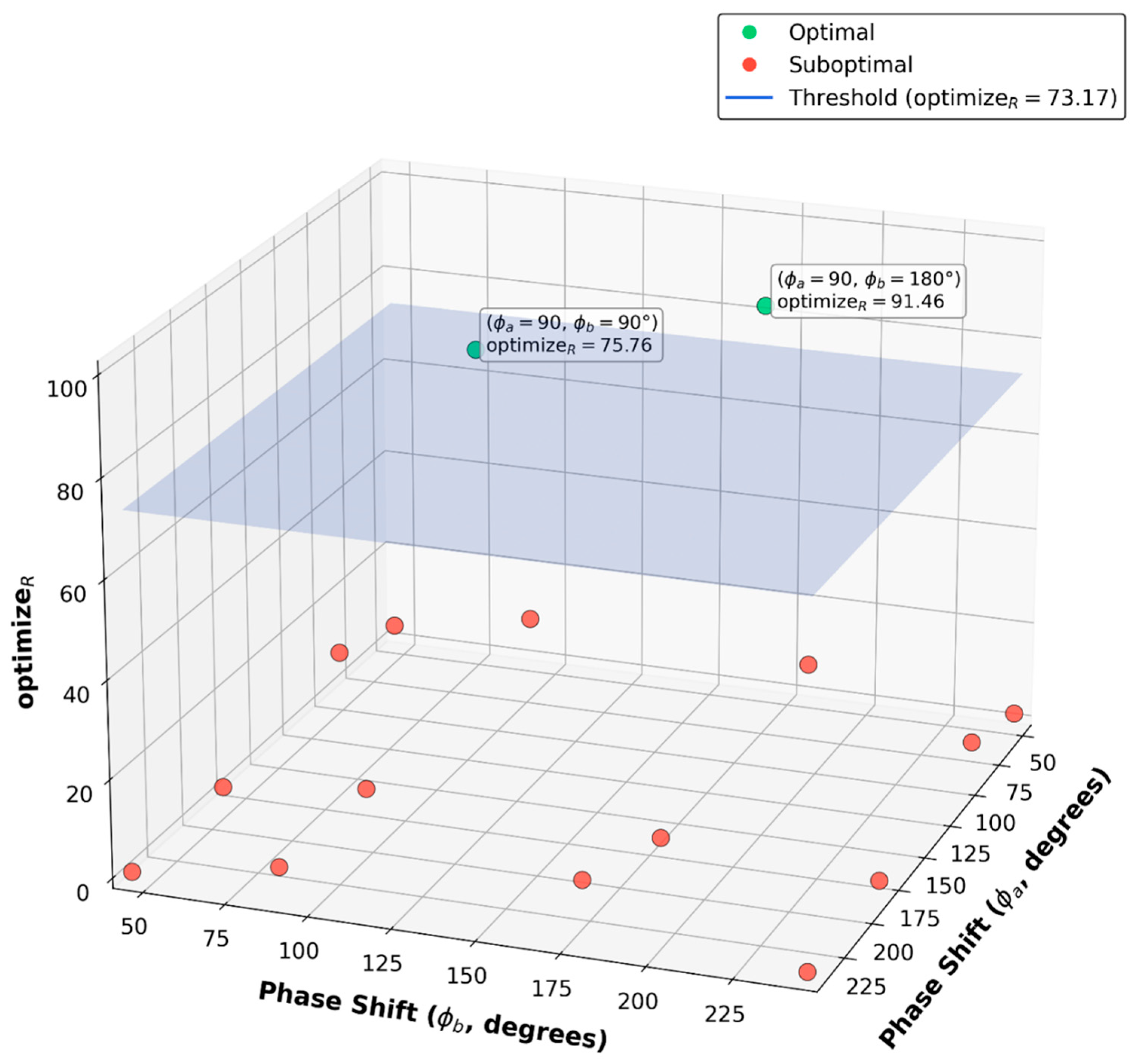
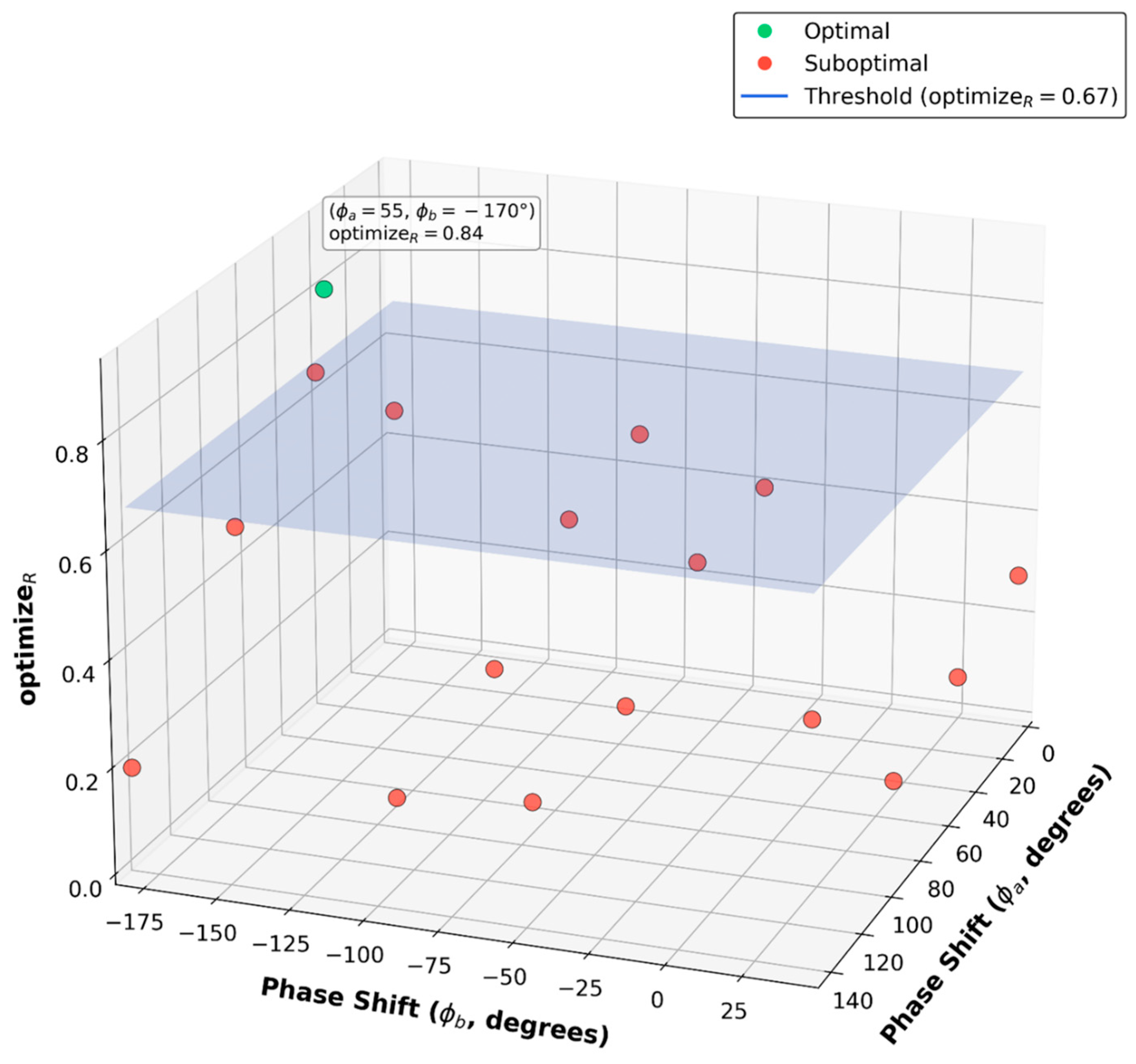
- Threshold Determination: A threshold for classification is established as 80% of the maximum value (). This dynamic approach adapts to the dataset’s range, though alternatives such as the median or a fixed value could be considered. (The thresholds of 73.17 (NOR) and 0.674 (NAND) were set at 80% of the maximum optimize_R values to visually distinguish near-optimal configurations in plots (e.g., Figure 3 and Figure 4). These thresholds are not essential, as ML-FOLD ranks configurations by optimize_R to identify the optimum without categorization.)
- For the NOR gate, the maximum was 91.46, resulting in a threshold of 73.17. For the NAND gate, the maximum was 0.843, yielding a threshold of 0.674.
- Classification: Each configuration is assigned a classification based on its value relative to the threshold.
- Final Stage: With the ranked results, we now have the best candidate, which has a high chance of being optimal, ready for final validation or implementation.
4. Results
4.1. NOR Gate Optimization
- ○
- The dataset comprised 16 phase pairs, with ranging from 0.275 to 91.46.
- ○
- Two configurations were classified as “Optimal”: (90°, 90°) with with = 91.46. The former aligns with this study’s reported NOR gate phases , producing outputs (0.6, 0.22, 0.20, 0.18), which correspond to NOR logic (1, 0, 0, 0) using thresholds of 0.5 for “1” and 0.3 for “0”. Figure 3 visualizes this, with annotated optimal points above the threshold plane.
4.2. NAND Gate Optimization
- ○
- The dataset included 17 phase pairs, with ranging from 0.162 to 0.843.
- ○
- One configuration was classified as “Optimal”: (55°, −170°) with , precisely matching this study’s NAND gate phases. The outputs (0.6, 0.53, 0.53, 0.2) align with NAND logic (1, 1, 1, 0) using the same thresholds.
- ○
- The formula accurately identifies a suppressed preds_AB_1 relative to the other states, validating its suitability for NAND optimization. Figure 4 illustrates this, with the annotated optimal point above the threshold.
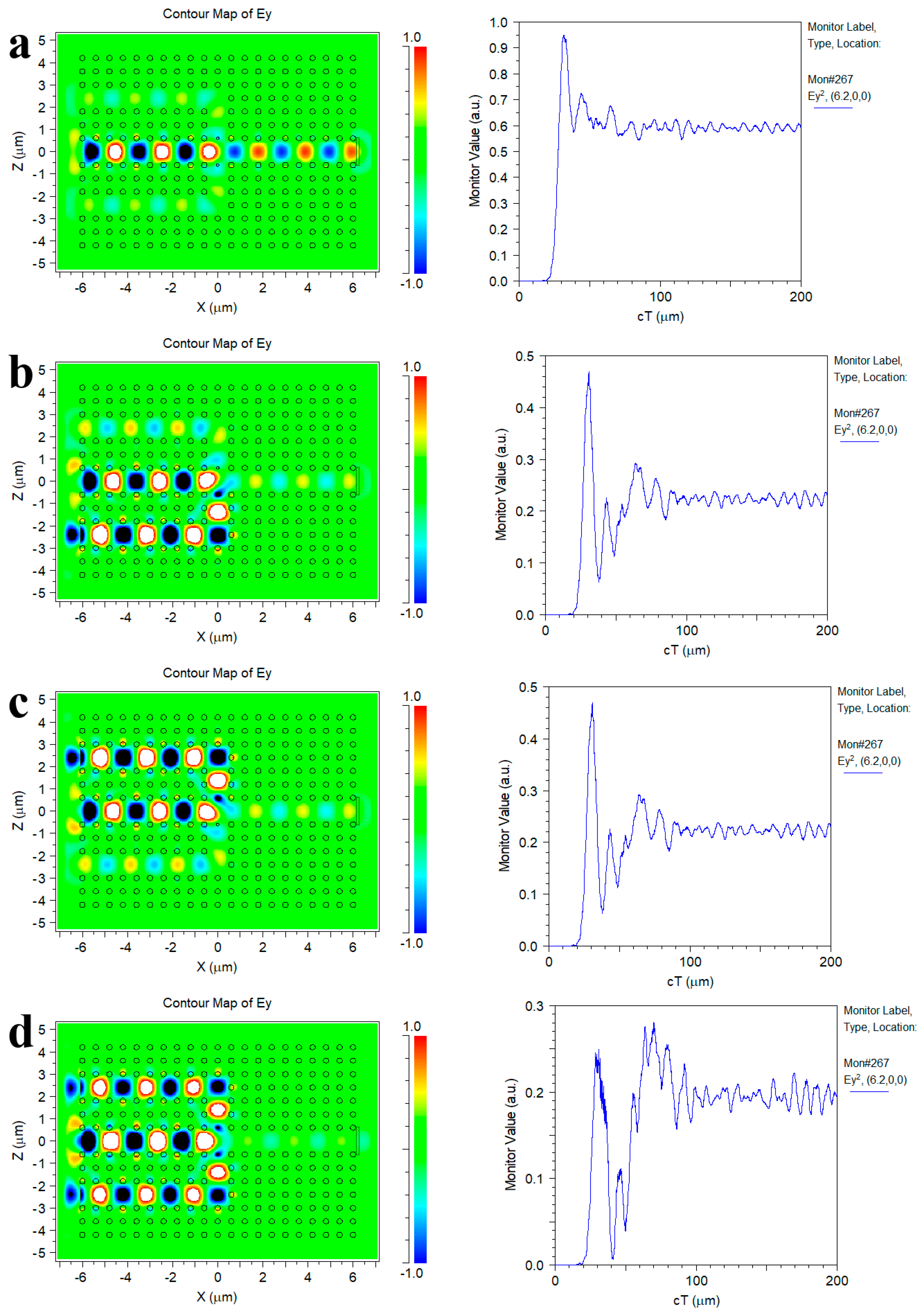
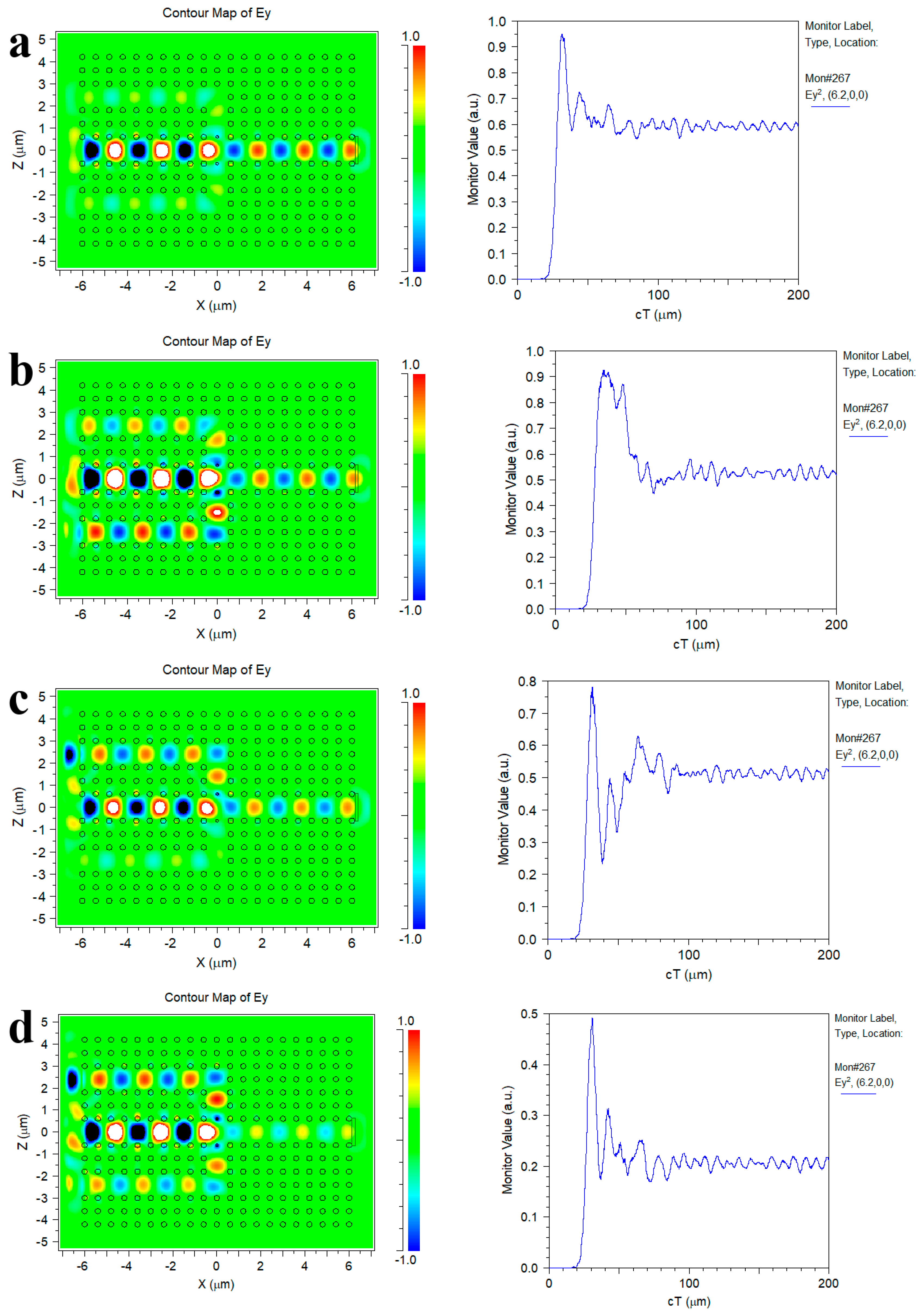
4.3. Simulation Results for the Optical NOR Gate
- Scenario a (A = 0, B = 0): When both input sources are inactive, the output is solely driven by the bias source, resulting in a normalized output power of 0.6, interpreted as a logical “1”.
- Scenario b (A = 0, B = 1): Activation of input B leads to destructive interference with the bias wave, reducing the output to 0.22, corresponding to a logical “0”.
- Scenario c (A = 1, B = 0): Similarly, activation of input A yields an output of approximately 0.2, due to destructive interference.
- Scenario d (A = 1, B = 1): When both inputs are active, combined destructive interference occurs, producing a minimal output of 0.18, also representing a logical “0”.
4.4. Simulation Outcomes of the Optical NAND Gate
- Scenario a (A = 0, B = 0): The absence of both inputs results in output power driven by the bias source, reaching 0.6, interpreted as logical “1”.
- Scenario b (A = 0, B = 1): With input B active, interference with the bias wave produces an output of 0.53, which is considered logical “1”.
- Scenario c (A = 1, B = 0): Input A is active, leading to a similar output of 0.53 due to the same interference conditions.
- Scenario d (A = 1, B = 1): Activation of both inputs results in strong destructive interference with the bias wave, reducing the output to 0.2, corresponding to a logical “0”.
5. Discussion
- FDTD iterative sweeps are computationally expensive and scale poorly with the number of parameters, as they lack a closed-form assessment metric.
- Genetic algorithms and ML models require extensive data and hyperparameter tuning, often leading to high computational costs and potential overfitting to simulation noise.
- ML-FOLD, in contrast, relies on only a small set of simulation results and uses simple arithmetic operations, allowing for rapid, interpretable evaluation of phase configurations.
6. Conclusions
Author Contributions
Funding
Institutional Review Board Statement
Informed Consent Statement
Data Availability Statement
Code Availability Statement
Conflicts of Interest
References
- Parandin, F.; Karami, P.; Mohamadi, A. Machine learning-driven optimization of photonic crystal structures for superior optical NOR gate performance. Appl. Opt. 2024, 63, 6666–6673. [Google Scholar] [CrossRef]
- Reuther, A.; Michaleas, P.; Jones, M.; Gadepally, V.; Samsi, S.; Kepner, J. AI and ML accelerator survey and trends. In Proceedings of the 2022 IEEE High Performance Extreme Computing Conference (HPEC), Waltham, MA, USA, 19–23 September 2022; IEEE: New York, NY, USA, 2022; pp. 1–10. [Google Scholar]
- Yablonovitch, E. Photonic crystals. J. Mod. Opt. 1994, 41, 173–194. [Google Scholar] [CrossRef]
- Brunner, D.; Shastri, B.J.; Qadasi, M.A.A.; Ballani, H.; Barbay, S.; Biasi, S.; Zhang, W. Roadmap on Neuromorphic Photonics. arXiv 2025, arXiv:2501.07917. [Google Scholar]
- Hazra, S.; Mukhopadhyay, S. Implementation of all-optical tristate Pauli X, Y and Z gates based on two-dimensional photonic crystal. Optoelectron. Lett. 2024, 20, 346–352. [Google Scholar] [CrossRef]
- Jalali Azizpour, M.R.; Soroosh, M.; Dalvand, N.; Seifi-Kavian, Y. All-Optical Ultra-Fast Graphene-Photonic Crystal Switch. Crystals 2019, 9, 461. [Google Scholar] [CrossRef]
- Rafiee, E. Bio-sensing applications of a 2:1 photonic crystal multiplexer. Sci. Rep. 2025, 15, 16840. [Google Scholar] [CrossRef]
- Mohammadi, A.; Parandin, F.; Karami, P. The ML-FOLD Method: Meta-Learning and Formula Optimization for All-Optical XOR, OR, and NOT Logic Gates. Available online: https://papers.ssrn.com/sol3/papers.cfm?abstract_id=5115354 (accessed on 5 May 2025).
- Joannopoulos, J.D.; Villeneuve, P.R.; Fan, S. Photonic crystals. Solid State Commun. 1997, 102, 165–173. [Google Scholar] [CrossRef]
- Djavid, M.; Dastjerdi, M.H.T.; Philip, M.R.; Choudhary, D.D.; Pham, T.T.; Khreishah, A.; Nguyen, H.P. Photonic crystal-based permutation switch for optical networks. Photonic Netw. Commun. 2018, 35, 90–96. [Google Scholar] [CrossRef]
- Rafiee, E.; Abolghasemi, F. An all-optical 1*2 de-multiplexer based on two-dimensional nonlinear photonic crystal ring resonators. Optoelectron. Lett. 2024, 20, 23–27. [Google Scholar] [CrossRef]
- Karami, P.; Mohamadi, A.; Parandin, F. Enhancing integrated optical circuits: Optimizing all-optical NAND and NOR gates through deep learning and machine learning. Opt. Quantum Electron. 2024, 57, 73. [Google Scholar] [CrossRef]
- Maleki, M.J.; Soroosh, M. An ultra-fast all-optical 2-to-1 digital multiplexer based on photonic crystal ring resonators. Opt. Quantum Electron. 2022, 54, 397. [Google Scholar] [CrossRef]
- Rafiee, E.; Afkhami, M. Design of an all-optical compact 2*1 multiplexer based on 2D photonic crystal ring resonators. Opt. Quantum Electron. 2024, 56, 283. [Google Scholar] [CrossRef]
- O′Halloran, M.; Conceicao, R.C.; Byrne, D.; Glavin, M.; Jones, E. FDTD modeling of the breast: A review. Prog. Electromagn. Res. B 2009, 18, 1–24. [Google Scholar] [CrossRef]
- Gangwar, R.K.; Pathak, A.K.; Kumar, S. Recent progress in photonic crystal devices and their applications: A review. Photonics 2023, 10, 1199. [Google Scholar] [CrossRef]
- Maleki, M.J.; Soroosh, M.; Akbarizadeh, G. A compact high-performance decoder using the resonant cavities in photonic crystal structure. Opt. Quantum Electron. 2023, 55, 852. [Google Scholar] [CrossRef]
- Serajmohammadi, S.; Alipour-Banaei, H.; Mehdizadeh, F. All optical decoder switch based on photonic crystal ring resonators. Opt. Quantum Electron. 2015, 47, 1109–1115. [Google Scholar] [CrossRef]
- Parandin, F.; Olyaee, S.; Heidari, F.; Soroosh, M.; Farmani, A.; Saghaei, H.; Karimzadeh, R.; Maleki, M.J.; Askarian, A.; Rahimi, Z.; et al. Recent advances in all-optical half-subtractor and full-subtractor based on photonic crystal platforms. J. Opt. Commun. 2024, 45, 2589–2618. [Google Scholar] [CrossRef]
- Swarnakar, S.; Kumar, S.; Sharma, S. Design of All-optical Half-subtractor Circuit Device using 2-D Principle of Photonic Crystal Waveguides. J. Opt. Commun. 2019, 40, 195–203. [Google Scholar] [CrossRef]
- Zhu, C.; Tian, L.; Cheng, W.; Gu, Z. Bio-inspired photonic crystals: Tailoring the dielectric building blocks to control the light propagation. BMEMat 2024, 2, e12056. [Google Scholar] [CrossRef]
- Huang, Y.; Shi, M.; Yu, A.; Xia, L. Design of multifunctional all-optical logic gates based on photonic crystal waveguides. Appl. Opt. 2023, 62, 774–781. [Google Scholar] [CrossRef]
- Mukherjee, B.; Kumar, V.D.; Gupta, M. A novel Hemispherical Dielectric Resonator Antenna on an Electromagnetic Band Gap substrate for broadband and high gain systems. Int. J. Electron. Commun. (AEU) 2014, 68, 1185–1190. [Google Scholar] [CrossRef]
- Rafiee, E.; Rafiei, E. Hypercholesterolemia diagnosis by a biosensor based on photonic crystal PANDA structure. Opt. Rev. 2024, 31, 87–93. [Google Scholar] [CrossRef]
- Rathi, S.; Swarnakar, S.; Kumar, S. Design of One-Bit Magnitude Comparator using Photonic Crystals. J. Opt. Commun. 2017, 40, 363–367. [Google Scholar] [CrossRef]
- Sharifi, H.; Maleknejad, M. Multi-functional all-optical photonic crystal logic gate using nonlinear directional coupler. Opt. Quantum Electron. 2021, 53, 673. [Google Scholar] [CrossRef]
- Surendar, A.; Asghari, M.; Mehdizadeh, F. A novel proposal for all-optical 1-bit comparator using nonlinear PhCRRs. Photonic Netw. Commun. 2019, 38, 244–249. [Google Scholar] [CrossRef]
- Firouzimoghaddam, A.; Sharifi, H. All-optical photonic crystal logic gates and functions based on threshold logic. J. Comput. Electron. 2025, 24, 10. [Google Scholar] [CrossRef]
- Rafiee, E. Photonic Crystal based Biosensor for Diagnosis of Kidney Failure and Diabetes. Plasmonics 2024, 19, 439–445. [Google Scholar] [CrossRef]
- Rachana, M.; Swarnakar, S.; Babu, M.R.; Swetha, P.M.; Rangaiah, Y.P.; Krishna, S.V.; Kumar, S. Optimization of an all-optical three-input universal logic gate with an enhanced contrast ratio by exploiting a T-shaped photonic crystal waveguide. Appl. Opt. 2022, 61, 8162–8171. [Google Scholar] [CrossRef]
- Farmani, A.; Mir, A.; Irannejad, M. 2D-FDTD simulation of ultra-compact multifunctional logic gates with nonlinear photonic crystal. J. Opt. Soc. Am. B 2019, 36, 811–818. [Google Scholar] [CrossRef]
- Swarnakar, S.; Palacharla, V.; Muduli, A.; Kumar, S. Design and optimization of photonic crystal based all-optical logic gate with enhanced contrast ratio. Opt. Quantum Electron. 2023, 55, 623. [Google Scholar] [CrossRef]
- Askarian, A.; Akbarizadeh, G.; Fartash, M. A novel proposal for all optical half-subtractor based on photonic crystals. Opt. Quantum Electron. 2019, 51, 264. [Google Scholar] [CrossRef]
- Wang, C.; Guo, X.; Wu, X. Electrically tunable graded photonic crystal lens based on graphene plasmons. Sci. Rep. 2024, 14, 26169. [Google Scholar] [CrossRef] [PubMed]
- Shaik, E.; Rangaswamy, N. Realization of all-optical NAND and NOR logic functions with photonic crystal based NOT, OR and AND gates using De Morgan’s theorem. J. Opt. 2018, 47, 8–21. [Google Scholar] [CrossRef]
- Rebhi, S.; Najjar, M. A new design of a photonic crystal ring resonator based on Kerr effect for all-optical logic gates. Opt. Quantum Electron. 2018, 50, 358. [Google Scholar] [CrossRef]
- Masoud, A.M.; Ahmed, I.S.; El-Naggar, S.A.; Asham, M.D. Design and simulation of all-optical logic gates based on two-dimensional photonic crystals. J. Opt. 2022, 51, 343–351. [Google Scholar] [CrossRef]
- Singh, J.J.; Dhawan, D.; Gupta, N. 2D photonic crystal hexagonal ring resonator-based all-optical logic gates. Opt. Laser Technol. 2023, 165, 109624. [Google Scholar] [CrossRef]
- Vadukanathan, A.; Suyambrakasam, G.; Sivaraj, P. Design of all-optical NOR and NAND gate using hybrid material corner scatters in photonic crystal ring resonators. Phys. Scr. 2025, 100, 045527. [Google Scholar] [CrossRef]


| Parameter | Index | Value |
|---|---|---|
| Lattice Constant | a | 0.6 µm |
| Radius of Rods | R | 0.12 µm |
| Refractive Index of Background | n1 | 1 |
| Refractive Index of Rods | n2 | 3.46 |
| Number of Rods | - | 21 × 15 |
| A | B | NAND | NOR |
|---|---|---|---|
| 0 | 0 | 1 | 1 |
| 0 | 1 | 1 | 0 |
| 1 | 0 | 1 | 0 |
| 1 | 1 | 0 | 0 |
| Input State | NOR Output (Binary Equivalent) | CR (NOR) | NAND Output (Binary Equivalent) | CR (NAND) |
|---|---|---|---|---|
| 00 | 0.6 (1) | 4.8 | 0.6 (1) | |
| 01 | 0.2 (0) | 0.53 (1) | 4.2 | |
| 10 | 0.2 (0) | 0.53 (1) | ||
| 11 | 0.18 (0) | 0.2 (0) |
| Ref. | Type | Size (µm2) | P0,max | P1,min | CR (dB) | Stable Time (ps) |
|---|---|---|---|---|---|---|
| [35] | NAND | 390 | 0.15 | 0.50 | 5.18 | 0.67 |
| NOR | 390 | 0.20 | 0.51 | 4 | 0.67 | |
| [36] | NAND | 396 | 0.28 | 0.75 | 4.25 | 6 |
| [37] | NAND | 98 | 0.17 | 0.43 | 4 | 0.32 |
| NOR | 98 | 0.21 | 0.43 | 3.1 | 0.32 | |
| [38] | NAND | 56 | 0.24 | 0.29 | 0.85 | 3.33 |
| NOR | 56 | 0.24 | 0.29 | 0.85 | 3.33 | |
| [39] | NAND | 280 | 0.03 | 0.11 | 5.6 | 2.5 |
| NOR | 280 | 0.04 | 0.34 | 9.2 | 2.5 | |
| This work | NAND | 100 | 0.20 | 0.53 | 4.2 | 0.32 |
| NOR | 100 | 0.20 | 0.60 | 4.8 | 0.32 |
Disclaimer/Publisher’s Note: The statements, opinions and data contained in all publications are solely those of the individual author(s) and contributor(s) and not of MDPI and/or the editor(s). MDPI and/or the editor(s) disclaim responsibility for any injury to people or property resulting from any ideas, methods, instructions or products referred to in the content. |
© 2025 by the authors. Licensee MDPI, Basel, Switzerland. This article is an open access article distributed under the terms and conditions of the Creative Commons Attribution (CC BY) license (https://creativecommons.org/licenses/by/4.0/).
Share and Cite
Mohammadi, A.; Parandin, F.; Karami, P.; Olyaee, S. Design and Optimization of Optical NAND and NOR Gates Using Photonic Crystals and the ML-FOLD Algorithm. Photonics 2025, 12, 576. https://doi.org/10.3390/photonics12060576
Mohammadi A, Parandin F, Karami P, Olyaee S. Design and Optimization of Optical NAND and NOR Gates Using Photonic Crystals and the ML-FOLD Algorithm. Photonics. 2025; 12(6):576. https://doi.org/10.3390/photonics12060576
Chicago/Turabian StyleMohammadi, Alireza, Fariborz Parandin, Pouya Karami, and Saeed Olyaee. 2025. "Design and Optimization of Optical NAND and NOR Gates Using Photonic Crystals and the ML-FOLD Algorithm" Photonics 12, no. 6: 576. https://doi.org/10.3390/photonics12060576
APA StyleMohammadi, A., Parandin, F., Karami, P., & Olyaee, S. (2025). Design and Optimization of Optical NAND and NOR Gates Using Photonic Crystals and the ML-FOLD Algorithm. Photonics, 12(6), 576. https://doi.org/10.3390/photonics12060576