Article

High-Performance NIR Laser-Beam Shaping and Materials Processing at 350 W with a Spatial Light Modulator

1
Laser Processing Research Laboratory, Department of Mechanical and Aerospace Engineering, School of Engineering, The University of Manchester, Manchester M13 9PL, UK
2
Laser Group, School of Engineering, University of Liverpool, Brownlow Street, Liverpool L69 3GQ, UK
3
James Watt School of Engineering, University of Glasgow, Glasgow G12 8QQ, UK
4
School of Engineering, Liverpool John Moores University, Tithebarn Street, Liverpool L2 2QP, UK
5
Hamamatsu Photonics UK Ltd., Welwyn Garden City AL7 1BW, UK
6
SEM Shared Research Facility, University of Liverpool, Liverpool L69 3GH, UK
7
Department of Materials, University of Manchester, Manchester M13 9PL, UK
*
Authors to whom correspondence should be addressed.
Photonics 2025, 12(6), 544; https://doi.org/10.3390/photonics12060544
Submission received: 27 April 2025 / Revised: 23 May 2025 / Accepted: 26 May 2025 / Published: 28 May 2025
(This article belongs to the Special Issue Fundamentals and Applications of Vortex Beams)

Abstract

:
Shaping or splitting of a Gaussian beam is often desired to optimise laser–material interactions, improving throughput and quality. This can be achieved holographically using liquid crystal-on-silicon spatial light modulators (LC-SLMs). Until recently, maximum exposure has been limited to circa 120 W average power with a Gaussian profile, restricting potential applications due to the non-linear (NL) phase response of the liquid crystal above this threshold. In this study, we present experimental tests of a new SLM device, demonstrating high first-order diffraction efficiency of η = 0.98 ± 0.01 at 300 W average power and a phase range Δφ > 2π at P = 383 W, an exceptional performance. The numerically calculated device temperature response with power closely matches that measured, supporting the higher power-handling capability. Surface modification of mild steel and molybdenum up to P = 350 W exposure is demonstrated when employing a single-mode (SM) fibre laser source. Exposure on mild steel with a vortex beam (m = +6) displays numerous ringed regions with varying micro-structures and clear elemental separation created by the radial heat flow. On molybdenum, with multi-spot Gaussian exposure, both MoO3 films and recrystallisation rings were observed, exposure-dependent. The step change in device capability will accelerate new applications for this LC-SLM in both subtractive and additive manufacturing.

1. Introduction

The ability to dynamically control the wavefront of a high-power laser beam is regarded as essential for future high-technology applications in laser–materials processing, such as the fourth industrial revolution (4IR), which includes breakthroughs in artificial intelligence (AI), automation, and advanced manufacturing technology. The 4IR involves the “integration of technologies across the physical, digital, and biological domains” [1,2]. In this regard, liquid crystal spatial light modulators (LC-SLMs) are ideal devices. As digital, programmable adaptive optics, they are able to modulate both phase/amplitude and polarisation with a high resolution to create the desired optical light fields. When addressed with appropriate computer-generated holograms (CGHs), incident light can be shaped to the required intensity distribution, including vector and scalar vortex beams with helical wavefronts, the latter carrying orbital angular momentum (OAM) where the light wave now carries Lz = mℏ/photon (m = topological charge), as well as spin angular momentum (SAM) carrying Sz = ±ℏ/photon when circularly polarised [3,4,5,6,7].
At lower powers, the breadth of current applications for SLMs ranges from classical and quantum computing [4,5], increased communications bandwidths [8,9], linear and NL optical microscopy [10,11], and Raman spectroscopy [12] to high-energy (HE) ultrafast pulse amplification [13,14,15,16] and materials micro-structuring [17,18,19,20,21,22,23,24,25,26,27,28,29,30,31,32,33,34,35]. Although nematic LC-based SLMs are typically limited to ≤50 Hz bandwidth, an unprecedented CGH address rate on a ferroelectric binary LC device at > 6 kHz was recently demonstrated [36]. As flat-top profiles are highly useful, for example, in thin film processing or HE laser-pulse amplification, a near-perfect uniform round flat-top profile with transmission > 92% was recently demonstrated when combining a refractive beam shaper and SLM for ultrafine intensity modulation [37]. In the case of high average power and high-throughput ultrafast parallel beam laser ablation, high quality can also be achieved using diffractive optical elements (DOEs) or beam modulation with acousto-optic and SLMs by careful process parameter optimisation [38].
With the introduction of liquid cooling, the power handling capability of LC-SLMs has steadily improved [39,40,41,42,43,44]; however, until recently, there has been a serious limitation on device performance due to the residual absorption in the SLM chip, with heat diffusing to the LC layer so that above P ~ 120 W with a Gaussian beam and 1/e2 beam diameter of D ~ 7 mm, the phase range drops dramatically, severely limiting diffraction efficiency [43]. By converting a Gaussian to a flat-top intensity profile with dimensions of ~8 × 8 mm at the SLM, reducing peak intensity and thermal gradients, the range was extended to P ~ 200 W average power when combined with an ultrafast laser system [44].
As the SLM has been the limiting factor in integration with higher-power laser manufacturing systems, the device physics and thermal management to handle much higher powers have required significant optical and thermal re-engineering [45]. The dielectric reflective multi-layer stack was altered to place the peak electric field within the lower index quarter wave (QW) layer, increasing the laser-induced damage threshold (LIDT) while the front window, previously of amorphous fused silica, has been replaced with single-crystal sapphire, which has a much higher thermal conductivity and comparable absorption coefficient α ~ 3 ppm/cm [46]. These critical developments increased the power handling capability by at least fivefold, a remarkable achievement. Hence, it is now possible to reach circa P = 700 W with full phase response from a 5.5 mm 1/e2 Gaussian beam [45]. This opens the door to many new possibilities in laser–materials processing, such as high-throughput, ultrafast materials micro-structuring [38] or with CW fibre laser sources, flexibly shaping the incident beam to optimise intensity distribution, for example in powder bed fusion [47,48] or laser welding [49]. A timely, recent review on progress in “high-power and high intensity structured light” created by direct intra-cavity or by external modulation, such as using LC-SLM and digital mirror devices (DMD), highlighted relevant application areas such as high-energy physics, quantum physics, optical communications, and material processing in manufacturing [50]. To enable applications, characterisation of the LC-SLM performance with increasing laser exposure is required prior to experiments on laser–materials modification. To the best of our knowledge, no such work has been published in the range above P ~ 200 W.
In this paper, we present detailed measurements of the phase response of a cooled SLM up to an average power of P = 383 W, the observed thermal response, and comparative numerical modelling and experimental results of efficient multi-beam and shaped-beam processing on metals with increasing average power up to P = 350 W.

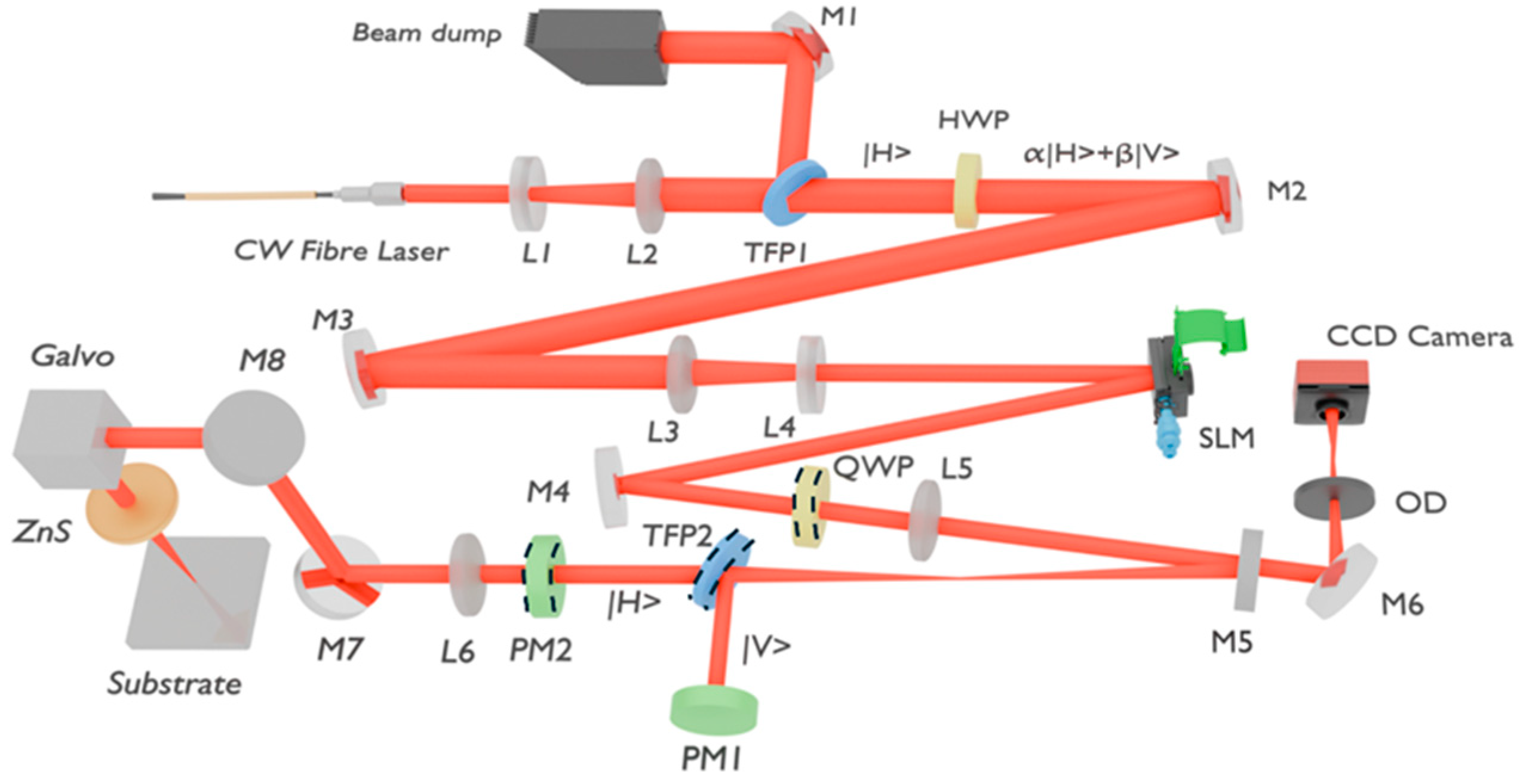
2. Materials and Methods

A schematic diagram of the experimental setup for measuring laser processing and phase response is shown in Figure 1. The collimated output from a high-power, single-mode CW fibre laser (YLR-1000-SM, IPG Laser, Coventry, UK, λ = 1070 nm, randomly polarised) was expanded ×2, and passed through a thin film polariser (TFP1, Altechna 2-HC45TPF-1064-0254,Vilnius, Lithuania) and a half-wave plate (HWP, Altechna 2-CPW-TZ0-L2-1064), transmitting ≈ 50% of the incident radiation in horizontal |H > polarisation while the unwanted vertical |V > polarised component was directed to a beam dump. After transmission through a reducing telescope (×0.5), the beam was directed to the liquid-cooled SLM (Hamamatsu X15213-03, 1280 × 1024 pixels, 12.5 μm pixel size, 255 addressable grey levels). On reflection from the SLM, a 4f optical system (f5 = f6 = 400 mm) re-imaged the modulated beams to a water-cooled scanning galvo (Scanlab Hurryscan 20, Puchheim, Germany) with a ZnS aspheric lens (f7 = 320 mm) for materials processing. To enable phase response measurements, a QWP (Altechna 2-CPW-TZ0-L4-1064) and thin film polariser (TFP2, Altechna 2-HC45TPF-1064-0254) separated orthogonally polarised components when incident linear polarisation was set to θ = 45.0° on the SLM by the HWP, along with the application of fixed grey-level (GL) CGHs. The transmitted |H> and reflected |V> components were measured by air-cooled power meters (Gentec UP55G-500F-H12, Quebec, QC Canada), while above P = 300 W, a kW level power meter (Gentec UP55C-2.5KW-HD-D0) was employed to measure transmitted power. To avoid potential damage to the TFP1 optic, the fibre laser beam was expanded from circa φ = 5.5 mm 1/e2 by ×2, hence requiring demagnification ahead of the SLM. The telescope lenses in the beam expander had f1 = −100 mm, f2 = 200 mm, and M = ×2, while in the reducing telescope, the lenses had f3 = 200 mm, f4 = −100 mm, and M = ×0.5, bringing the beam diameter close to the original. While telescope lenses were initially made from BK7, these were replaced by UV-grade fused silica, AR-coated (Newport/Optoman).
A Spiricon CCD camera was placed near the focal plane of the 4f lens, L5. The low-intensity beam transmitted through M5 was directed to the CCD. Thus, one could observe the multi-beam/shaped-beam intensity distribution during laser processing. OD filters allowed attenuation of this monitor beam as laser powers were increased.
Optical microscopy (Nikon, Tokyo, Japan) and a Keyence digital microscope, VHX-X1, (Osaka, Japan) were used for 2D/3D surface imaging as well as white-light interferometers (Polytec GmbH TMS-A-MVS-01, Waldbronn, Germany, WYKO 1100 (New York, NY, USA). For SEM imaging, we used a Zeiss Gemini 450 (FEG-SEM) and an EDX (Oxford Instruments X-Max 50 mm2 EDX detector, Abingdon, UK) for surface elemental measurements.

3. Results

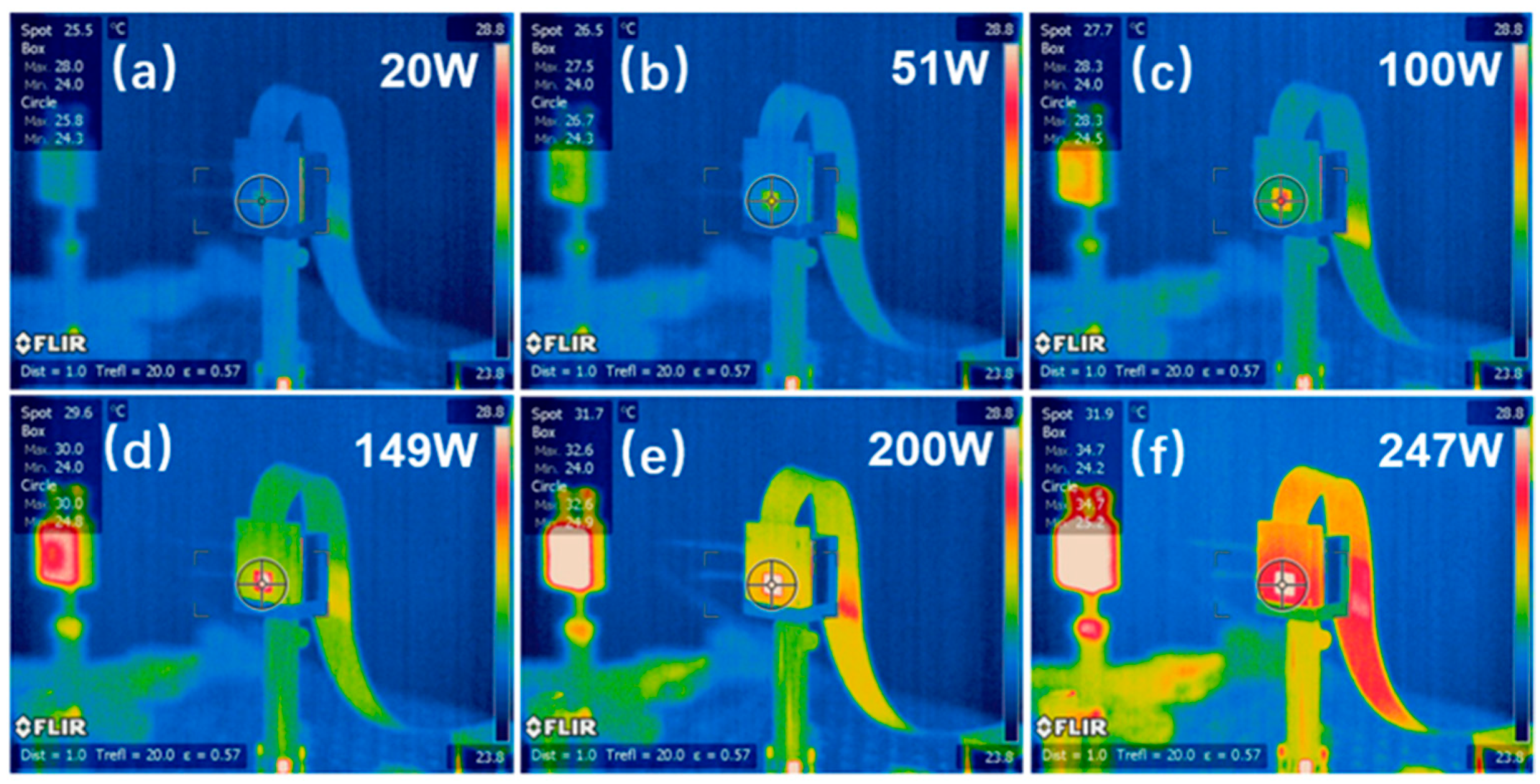
3.1. Chip Temperature with Exposure

The SLM reflectivity with the Gaussian beam was measured to be R = 0.98 ± 0.01 with 24 W exposure. This is in accord with the device specification [51]. The observed temperature profiles of the SLM chip measured with a FLIR SC660 thermal camera (Wilsonville, OR, USA) are shown in Figure 2a–f over the range 20 W ≤ P ≤ 247 W. A calibration test of the FLIR camera was implemented by measuring both the temperature of boiling water and melting ice when setting the emissivity to ε = 0.96 for distilled water. This simple test confirmed the recorded absolute temperatures to be accurate to <1 °C in this temperature range. The beam profile at the SLM was measured at low power (P ~ 1 W) with a copper pinhole centred on the beam, yielding D (1/e2) = 6.7 ± 0.1 mm. Up to 51 W exposure, the chip temperature appears quite uniform, as seen in Figure 2a,b. However, at about 150 W, a round central spot has a temperature differential and is higher than the rest of the chip by approximately 1.5 °C; hence, a thermal gradient exists (Figure 2d). At 200 W exposure, the whole chip reaches approximately uniform temperature due to thermal diffusion and effective cooling of the micro-structure by the liquid-cooled copper heat sink. At 247 W exposure, the chip temperature reached almost 32 °C (Figure 2f). The emissivity was set to ξ = 0.57, relevant to single-crystal sapphire [52].
Figure 3 shows the measured front-window peak temperature with exposure using a FLIR 660 thermal camera, which is linear. The estimated temperature gradient is δT/δP = 0.035 °C/W. This value is close to that observed previously on a cooled X10468-03 model [43]; however, the high thermal conductivity of sapphire implies that the front surface temperature more likely reflects the LC temperature—approximately 33.5 °C with 250 W exposure—still well below the critical temperature for the nematic–isotropic phase transition, Tc > 65 °C [43]. Nematic LCs tend to have their anisotropic molecules aligned in the same direction (termed the director), so that they have a long-range directional order. The resulting birefringence, which can be controlled by an electric field, is employed to alter the wavefront. Each pixel in the SLM can be individually addressed, hence yielding the required diffraction pattern. The LC temperature rises with increasing laser exposure, and eventually, thermal agitation leads to the complete loss of this order and birefringence; hence, a transition to an isotropic phase results, with complete loss of birefringence and beam-shaping ability.

3.2. Numerical Modelling of SLM Chip Temperature with Laser Exposure

With the aid of COMSOL multi-physics, (v 6.2) taking into account the physical details of the SLM micro-structure known to us, including a 2 mm thick sapphire window, we have numerically calculated the expected temperature rise of the LC layer and the front surface of the sapphire window with increasing power in a Gaussian intensity distribution. The calculation takes into account the SLM window, micron-thick alignment layers, LC layer, dielectric mirror with reflectivity R = 0.98, CMOS chip, ceramic cooling plate (SiN, 2 mm thick), and the 15 mm thick water-cooled copper heat sink with a flow rate of 2 L/min.
To achieve an accurate thermal computation, a non-uniform mesh grid with 1 mm (minimum) and 5 mm (maximum) element size was utilised, depending on the component layer within the SLM structure, optimising computational efficiency while capturing key thermal gradients. The simulation used the heat transfer in solids/fluids and turbulent flow package, ensuring a comprehensive evaluation of heat dissipation mechanisms.
Figure 4a–f shows the calculated 2D temperature distribution of the front sapphire window surface at thermal equilibrium with exposures of 50 W ≤ P ≤ 383 W and a D = 6.5 mm (1/e2) beam. The profiles reflect the spherical symmetry of the incident Gaussian beam.
Figure 5a–f shows the calculated temperature profile across the CMOS chip centre line for both the LC layer and sapphire window after reaching thermal equilibrium, while Figure 5g shows the simulated maximum temperature Tmax at the chip centre with exposure. A Gaussian beam with a diameter D = 6.5 mm 1/e2 is assumed. As expected physically, the LC temperature exceeds that of the front window while the temperature gradient is linear with exposure, (δT/δP)LC ~ 0.08 °K/W. For the sapphire window, the gradient (δT/δP)S = 0.034 °K/W, in excellent agreement with the experiment, Figure 3. The profiles show a peaked distribution in accordance with the incident Gaussian intensity distribution. The LC layer temperature exceeds that of the sapphire front surface by approximately 10 °C at P = 250 W.
The calculated dynamic temporal response of the LC layer and sapphire window is also of great interest; see Figure 6a,b with P = 250 W exposure, which highlights the rapid temperature rise of the LC after laser exposure, δT/δt ~ 7.5 °K/s, followed by a slower rise to equilibrium over approximately δt = 20 s due to thermal diffusion to the large thermal mass of the CMOS structure with the water-cooled heat sink. The sapphire, having a much higher thermal mass than the LC, reaches thermal equilibrium on the same timescale with a much slower δT/δt ~ 0.9 °K/s response after laser exposure. Heat diffusion takes place in both directions from the LC layer. The effect of altering the beam diameter, hence intensity, on the SLM yields realistic physical results with Figure 6a, D = 6.5 mm, and Figure 6b, D = 4.4 mm 1/e2 diameter, primarily increasing the LC temperature.

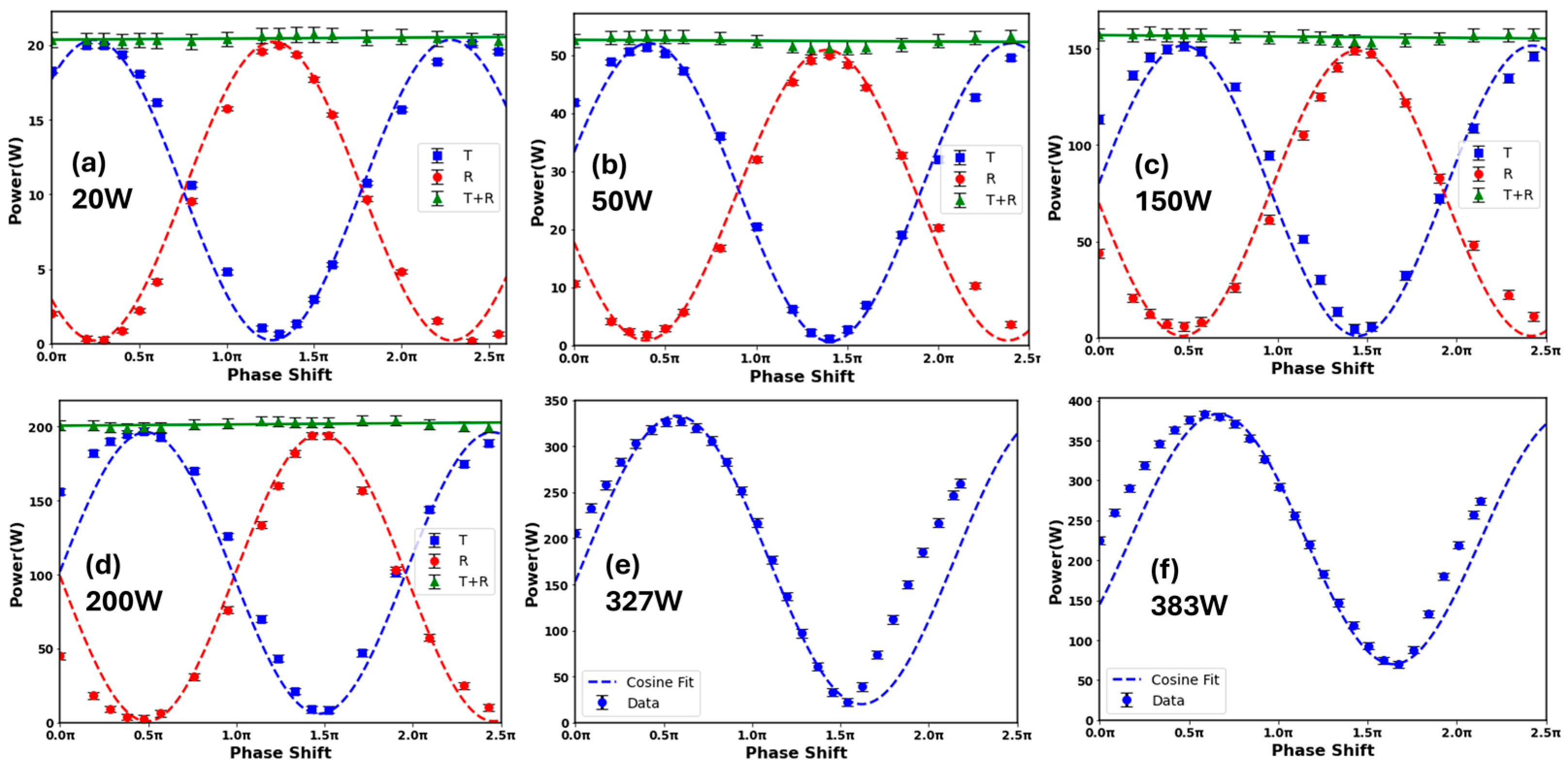
3.3. Phase Response with Exposure

With the incident linear polarisation set to θ = 45° AOI relative to the SLM director, the QWP was set to φ1 = 45° (relative to horizontal) + TFP2 tilted to φ2 = 45° (relative to optic axis), and the phase response was measured while altering the grey level (GL) of uniform CGHs applied. The reflected states of polarisation (elliptical and GL dependent) are converted to linear polarisations by the QWP, which rotates with applied GL and is analysed by the TFP2. In this case, we set the SLM blazing function to be 255:255, hence there is no pre-set calibration of the applied GL. This means a GL value of 255 will produce the maximum phase delay achievable by the SLM rather than a calibrated 2π phase shift. The observed responses with exposure, i.e., the transmission/reflection from TFP2, are shown in Figure 7a–f. On the horizontal axis, GLs are converted to phase shift φ in radians and calibrated so that the value 2π is achieved once the measured transmitted/reflected powers return to their original values at GL = 0. This range increased from Δ(GL) = 200 at 20 W to 239 at 383 W.
The measured data are shown along with the fits to ideal transmission/reflection functions (DOP < 1), T (φ) = Acos2[(φ − φ0)/2] + B, and R (φ) = A’ sin2 [(φ φ0)/2] + B’ for a linear response. These confirm that the phase range Δφ > 2π even at 383 W, which is already a factor of 3 higher than with a Gaussian beam on previous SLM models [43], and the DOP = (Pmax Pmin)/(Pmax + Pmin) = A/(A + 2B) = 1/(1 + 2B/A). A deviation from a linear response is already evident at 200 W below φ = 0.5π, while at 327 W and 383 W, the observed phase shifts deviate further, along with a drop in DOP. These power-dependent non-linear (NL) deviations of the optical response may occur in the polarising optics as well as from the SLM itself.
The measured reflected degree of polarisation, DOP, with power, calculated from the data and fits, is summarised in Figure 8. DOP = 0.97 ± 0.01 for P ≤ 280 W, while above 300 W, the DOP drops rapidly, reaching 0.69 at P = 383 W. Error bars represent 1σ.
This significant drop in DOP above P = 300 W signifies that something is amiss here. At P = 407 W, TFP1 suffered catastrophic damage simultaneously with AR coating damage on lens L1 of the expanding telescope. The ensuing thermal absorption when the concave lens AR coating exceeded its LIDT likely resulted in thermal lensing, reducing beam diameter, hence increasing peak intensity on TFP1 above the LIDT for the polarising film. These optics were replaced with products from Optoman [53], which may well have higher LIDTs. The QWP/TFP2 may also be under stress.
Thermal lensing can occur not only from the low absorption in transmissive fused silica optics, but also from the AR coatings, which require careful design to minimise absorption [54,55]. The decision here to expand the fibre laser beam to reduce peak intensities, followed by a reducing telescope ahead of the SLM, added to possible sources of thermal lensing in the telescope and polarising components. Thermal lensing was apparent when observing the low-angle off-axis SLM thermal image from the FLIR camera when increasing the laser power. The effective spot size was reduced to approximately 4.5 mm (estimated) with a hot centre. The CCD camera images also displayed this lensing effect, so that the camera required displacement towards the focal point as powers were increased. We observed a focal shift Δs300 W ~ 80 mm towards the first 4f lens L5 (f5 = 400 mm); hence, using the thin lens equation, we can estimate an “effective” focal length of the thermal lens at P = 300 W (600 W from the fibre laser) to be fth ~ 1.6 m.
For a given optical element, the focal shift Δf relative to the Rayleigh length Zr can be estimated by [55], ( Δ f Z r ) = ( D *   P a v ) / λ M 2 where D* is a lens-specific constant, and Pav is the average power exposure. For UV-fused silica with an anti-reflection (AR) V coat, D* = ~0.5 × 106 mm/W. For comparison, D*BK7 (V coat) = ~1.93 × 106 mm/W. On the other hand, for a neutral density filter, D*ND = ~3.32 × 104 mm/W, two orders of magnitude higher. If we compare the product ( D *   P a v ) for fused silica and our ND filter, allowing for a 0.1% transmission of mirror M6, the ratio (D* P)FS/(D* P)ND = ~1.6 at P = 300 W, but as the ND filter is much nearer lens L5’s focal plane, where the beam diameter is much smaller, thermal lensing from the ND filter could well contribute much more to the observed focal shift on the CCD.

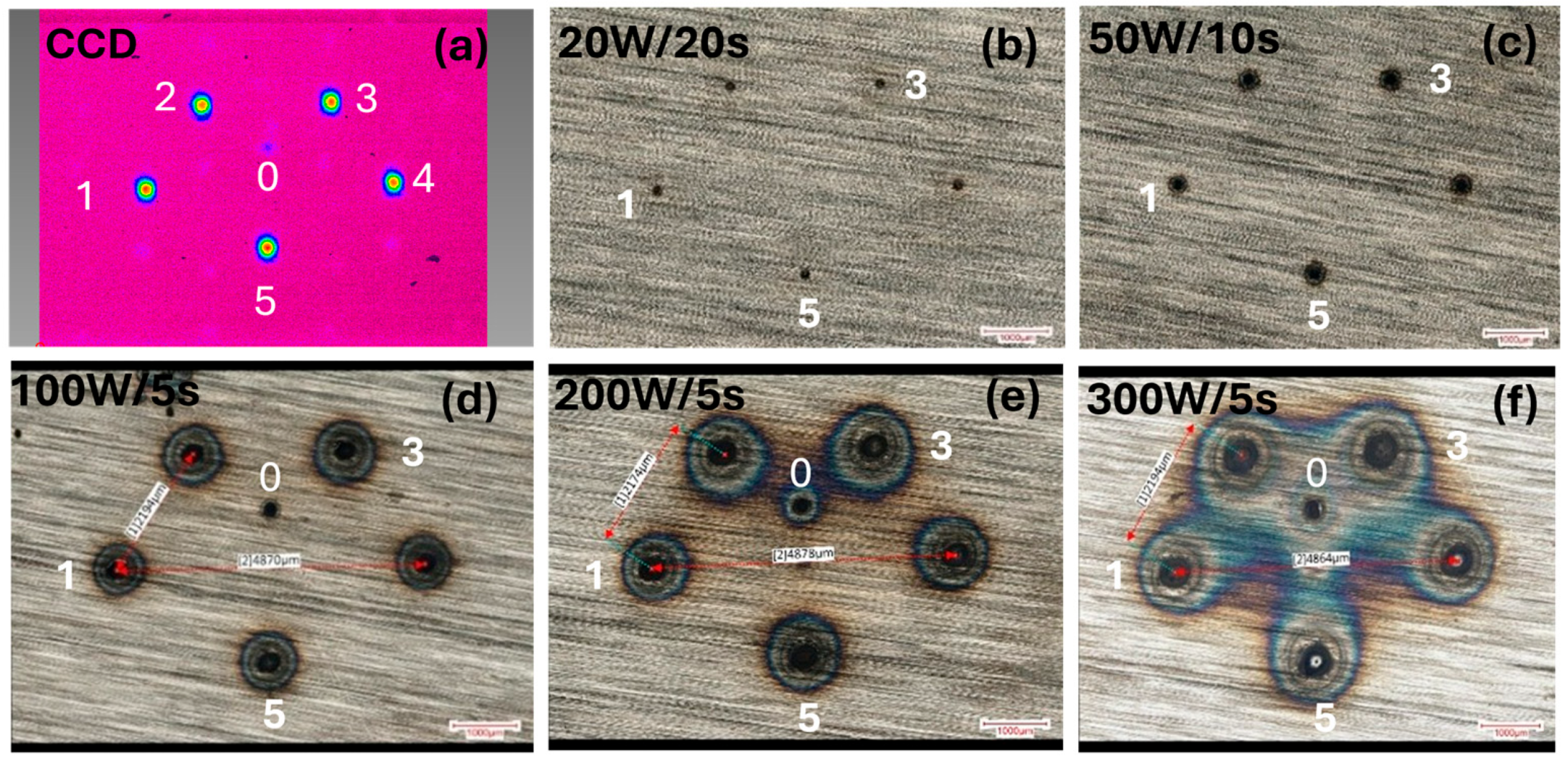
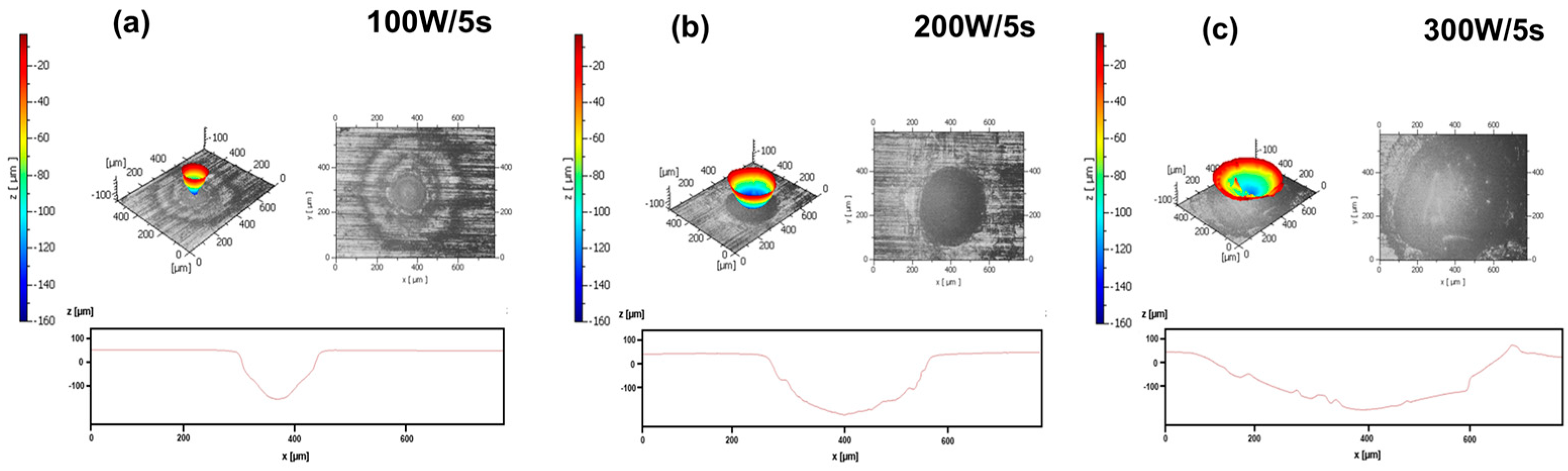
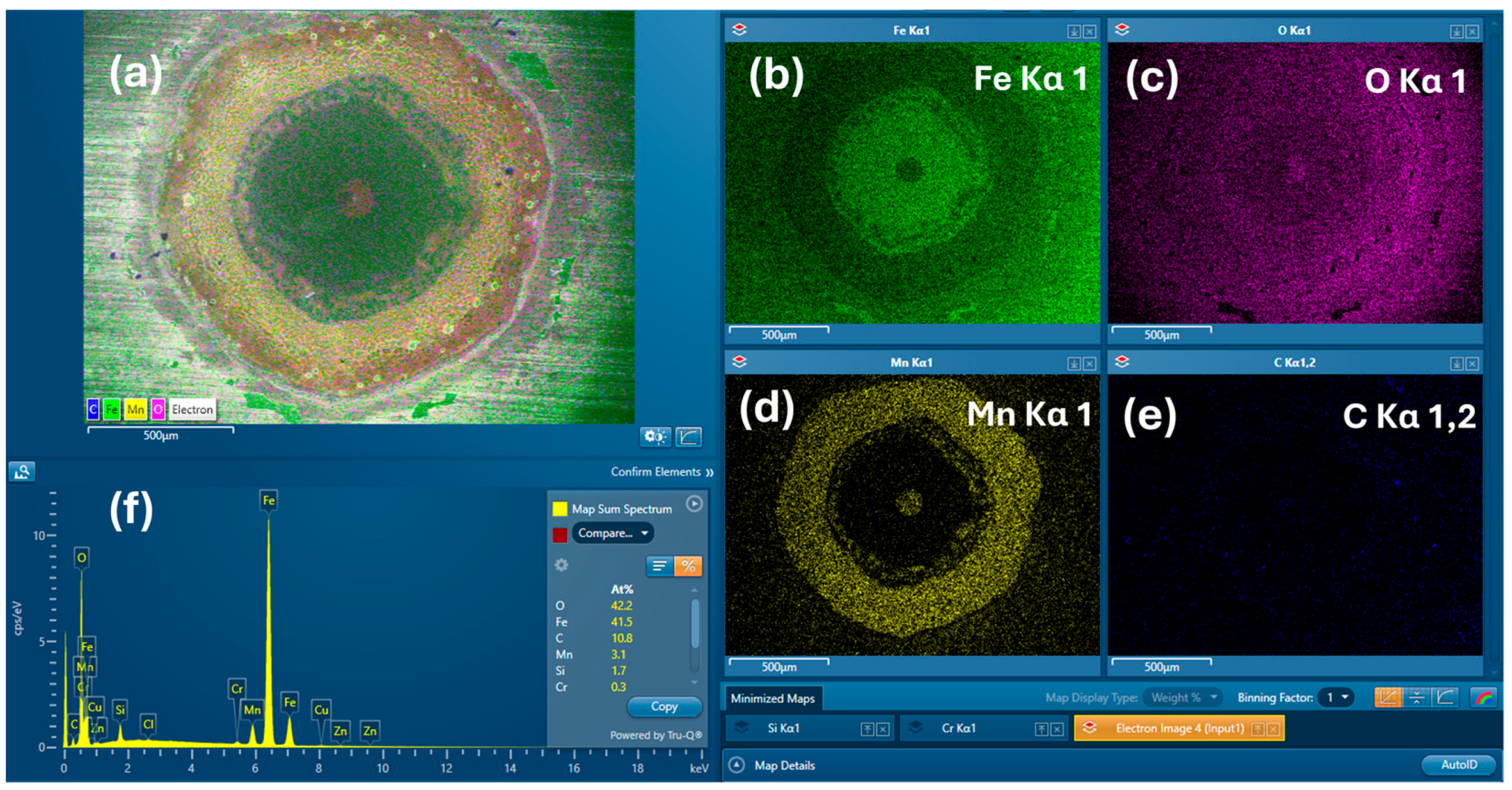
3.4. Multi-Spot Blind Drilling, Mild Steel

With QWP/TFP2/power meters removed, polished mild steel samples (10 cm × 10 cm × 1 cm), Ra = 1.4 ± 0.3 μm, were exposed to the modulated beams with the 4f system bringing the reflected complex E field after the SLM to the galvo input aperture. An aspheric ZnS lens (f = 320 mm) brought the diffracted beams to focus on the substrate mounted on a vertical table. ZnS has a much higher thermal diffusivity than fused silica, while thermal lensing for this element matches that of fused silica at high powers [56]. The transmission from the 4f lens L6 to the substrate was measured to be T = 0.98 ± 0.01. This is very satisfactory, allowing for four mirror reflections (periscope and galvo x, y) plus two AR-coated lenses (4f and aspheric focus lens), hence reflection loss R ≤ 0.25% per optical surface.
Figure 9a–f shows images of a five-spot (Gaussian) blind drill pattern machined on mild steel with CGH generated by the Gerchberg–Saxton (GS) iterative algorithm [57]. Before processing, the CCD camera image of spot separations is shown in (a). Power and exposures ranged from 20 W/20 s (b), 50 W/10 s (c), 100 W/5 s (d), 200 W/5 s (e), and 300 W/5 s (f). Uniformity from ablated crater volumes yields <U> = <(1 σ(V)/V)> = 0.72 ± 0.04 over 200–300 W, while a weak zero order appears at P ≥ 100 W. The measured first-order diffraction efficiency over the range 200 ≤ P ≤ 300 W, based on observed evaporated volumes, including zero order, yields DE, η = 1 ( V ( 0 ) / ( n = 0 n = 5 V ( n ) ) = 0.98 ± 0.01, where V(0) is the zero-order evaporated volume; a satisfactory result. The contribution diffracted to higher orders also appears to be low, as seen in Figure 9a. The thermal diffusion between spots is apparent from the observed surface colouration in Figure 9f, where the surface colouring around and between spots highlights the surface tempering due to the transient temperature field. Blue/purple implies that these regions have reached 250–300 °C [58]. The average focus spot ellipticity from the ratio of the semi-minor radius/semi-major radius was <ξ> = 0.88 ± 0.04 over the range of 50 W–300 W. The total evaporation rate on mild steel for a 5 s exposure with a five-spot pattern at P = 300 W, δV/δt ~ 0.7 mm3 min1, which was low due to significant thermal diffusion during exposure.
Figure 10a–c shows typical 2D/3D profiles of blind drilled spot geometries at total powers P = 100 W, 200 W, and 300 W, respectively (five-spot, 5 s exposures) with evaporated volumes/spots measured to be 309 ± 70, 2221 ± 690, and 4429 ± 1208 μm3 W1 s1, respectively. Variations are therefore approximately 25–30%. Burrs here appear minimal, while profile width increases significantly, a possible sign of thermal lensing in the optical system.
The average spot ellipticity <ξ>1–5 = <(Rmin/Rmax)> and evaporation volume rates, μm3 W1 s1 per spot, are summarised in Table 1. The large uncertainty here in evaporation rates (1σ) is connected with CW exposure, creating melting, plasma absorption, and the variation in spot uniformity.

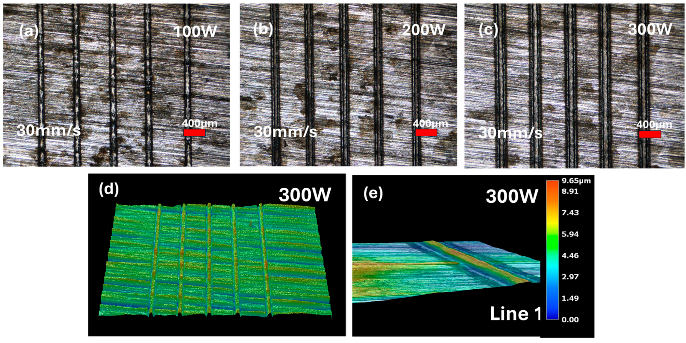
3.5. Multi-Beam Surface Scanning, Mild Steel

Figure 11a–c shows optical images of five parallel spot scanning on mild steel with power P = 100–300 W, a scan speed of 30 mm/s, and 10 overscans. Processing here demonstrates that the effect of zero order is insignificant with high first-order diffraction efficiency approaching unity, η ~ 1. The spot pattern was created in the LabVIEW software (v. 2022 Q3) interface with the Roberto–GS algorithm [59]. The surface has been melted and tends to rise above the pristine surface due to melt flow during exposure, mainly driven by surface tension, which depends on the temperature gradient created by the heat source and the material’s thermal properties. Thus, the amount of surface rise gives an indirect indication of the effect of the laser beam profile and its imposing thermal attributes. Figure 11d presents a 3D Wyko image of the scanned lines, while Figure 11e shows a higher magnification profile of a single line.

3.6. Vortex Beam Processing, Mild Steel

By using CGHs with an azimuthal phase variation, φ = e-imθ, we generated ring modes with a helical wavefront, m = ± 6, carrying orbital angular momentum, OAM. The expected intensity profile for |m| = 6 is given by [3],
I = I 0 ( 2 6 / 6 ! ) ( r 12 / ω 0 12 ) e x p ( 2 ( r 2 / ω 0 2 ) )
where I0 is the initial Gaussian peak intensity with 1/e2 radius ω0, while the radius at which the ring intensity is maximum is given by Rmax = 3 ω 0 . The ring peak intensity is given by I p e a k = 6 6 I 0 / ( 6 ! e 6 ) = 0.16 I 0 . Figure 12a shows the 2D intensity cross-section expected for m = 6, where the ring peak reaches 16% of the Gaussian peak intensity, set here to unity. The calculated 3D ring beam intensity in MATLAB (v.2022b) is shown in Figure 12b.
Average powers in the range of P = 100–350 W were used with a 1 s exposure. The observed resulting micro-structure at the highest power exposure was found to be most interesting and is reported here in Figure 13a–f. Figure 13a shows an optical image of the surface modification of mild steel with 350 W/1 s exposure and a ring mode m = 6 vortex beam. Spiricon’s image of the m = 6 vortex beam at the 2f plane is shown in Figure 13c. Figure 13b,d shows higher magnification images of the complex circular symmetry which developed during exposure. There is a definite component of hexagonal symmetry in Figure 13a; however, this may be connected with the ring intensity asymmetry, as seen in Figure 13c. The results are interesting, as five regions with different surface micro-structure are discernible. At the centre, individual single micro-crystals are evident within a radius r1 ~ 65 μm surrounded by a circular reflective region with a radius r2 ~ 290 μm, while radial cracks are also apparent here, then three additional thin ring regions which appear out to r5 = 680 μm. The dark-ringed, highly oxidised region, Figure 13a, corresponds to the ring intensity diameter, D ~ 1.0 mm.
SEM imaging yields complementary data to those from optical imaging, while EDX yields surface layer elemental analysis, as seen in Figure 14a. The cylindrical symmetry already observed is confirmed, while the elemental composition shows remarkable evidence of elemental segregation. Figure 14b shows that the Fe concentration drops both at the centre and in the ring intensity region due to significant oxidation there. In this hexagonal region, the Mn atoms appear to have diffused here as well as at the centre, as in Figure 14d. The average EDX elemental concentrations are shown in the EDX spectrum, also in Figure 14f. Strong Mn segregation can be linked to the unique vortex ring beam intensity profile, which influences how energy is delivered to the mild steel surface. This intensity profile creates temperature gradients within the small molten metal pool, generating considerable surface-tension-driven flow at the scales, observed in Figure 14. As Mn is rejected from the solidifying phase, it is transported by this flow and accumulates in the regions which solidify last. Additionally, higher Mn concentrations can lower the local equilibrium melting point, further influencing segregation patterns. While these effects suggest strong links among beam profile, induced flow, material characteristics, and metallurgical behaviour, a detailed investigation of liquid metal transport mechanisms at the sub-millimetre scale is required for the future.
This hexagonal symmetry developing on the mild steel surface was quite unexpected with a ring mode. However, the m = 6, CCD profile also displays aspects of this symmetry, possibly due to phase discontinuity at 0/2π transitions, which may account for this observation. The ring mode creates radial thermal diffusion inwards and outwards.

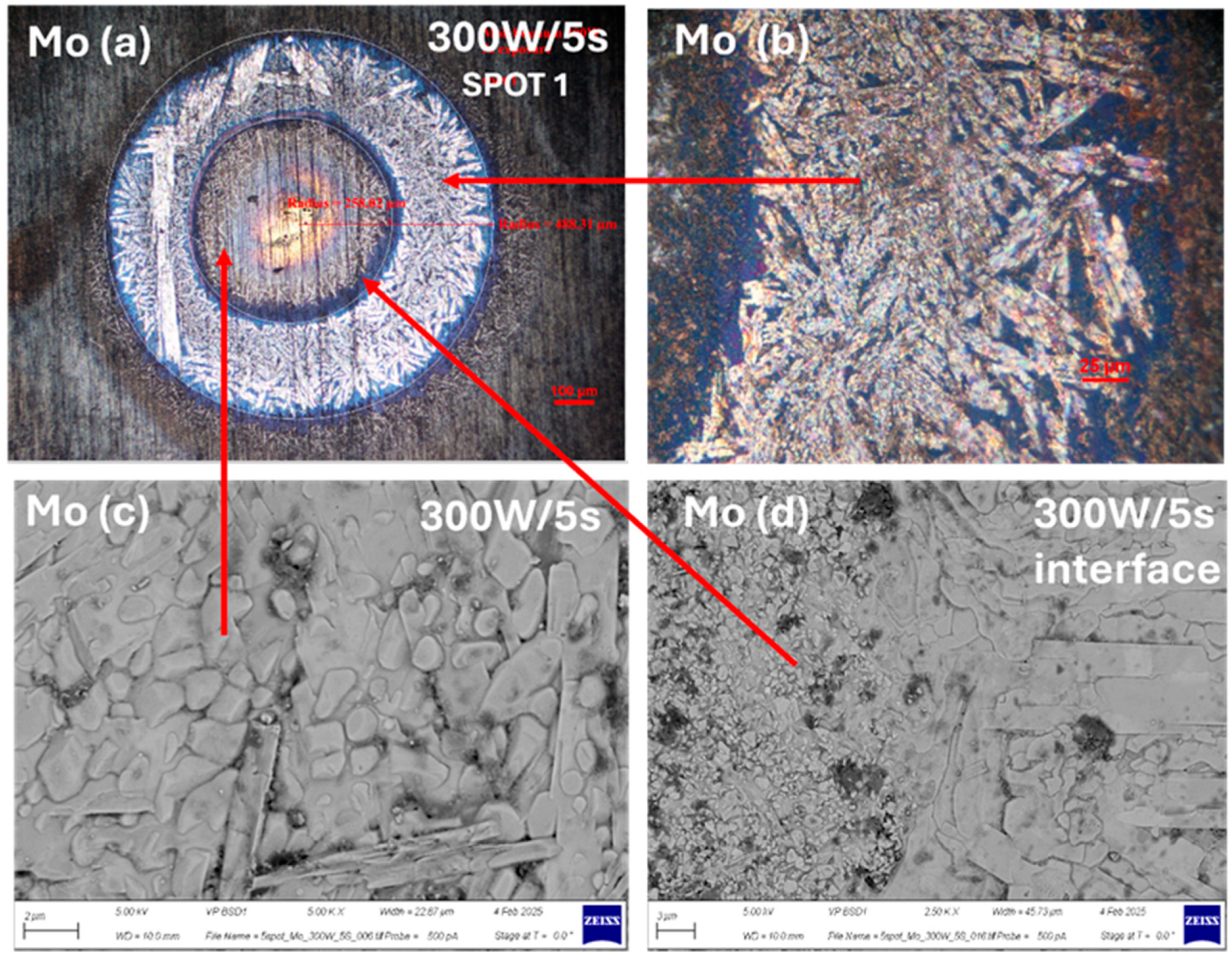
3.7. Multi-Beam Exposure, Molybdenum

Molybdenum has the third-highest melting point of all metals, Tm = 2622 °C, a boiling point Tevap = 4639 °C [60,61], density ρ = 10.2 gcm3, and relatively high thermal diffusivity, D = 0.55 cm2 s1 at room temperature, decreasing monotonically to D = 0.21 cm2 s1 at T = 2200 °C [62,63]. The five-spot pattern was next applied to pure molybdenum (50 × 50 × 1 mm) with a surface roughness Ra = 0.48 ± 0.04 μm. Figure 15a–d shows the results with 300 W/1 s exposure. Figure 15a shows a tilted 3D digital optical image of the five-spot pattern, while Figure 15b shows an optical image of a single spot, highlighting the yellow/gold oxidised surface observed in reflection, likely the formation of a thin film of MoO3 [64]. Mo is evaporated out to a radius r1 ~ 30 μm, while the oxidised region extends out to r2 ~ 70 μm. Figure 15c shows a combined SEM and EDX elemental map, while Figure 15d shows the EDX spectra of the Mo and O elemental fractions, confirming that at the centre (Spectrum 1), the oxide is MoO3, a semiconductor. MoO3 can also be produced by high-repetition-rate (MHz), low-energy (nJ) fs laser exposure on Mo in air [65,66].
Figure 16a,b and Figure 16c,d are optical and SEM images, respectively, of a 5 s/300 W exposure on pure Mo (five-spot pattern) showing a gold spot at the centre with two surrounding ringed regions, the inner ring containing micron-sized and slender rod-like crystals. The outer ring has an inner radius R2 ~ 260 μm and outer radius R3 ~ 490 μm. Figure 16c shows an SEM image of the first ring, while Figure 16d shows the boundary region between the rings. The recrystallisation takes place after the laser is switched off rapidly, effectively quenching the material. Note also the intense blue colour (molybdenum blue) which appears at the periphery and the inner boundary of the outer ring. This is likely an oxide of molybdenum, termed Mo5O14xH2O, the monohydrate suggesting that a reaction with water vapour in the air may also have occurred [67].

4. Discussion and Conclusions

Current and future industrial laser applications require high-efficiency, high-throughput surface processing at multi-hundred-watt and kW levels, since these average power levels are already available [68,69,70,71]. A device which can dynamically structure the optical field for different applications is therefore highly useful for optimising any given laser-surface process, whether ultrafast ablation [38], CW thermal exposure for AM [48], or materials welding where the Gaussian profile is far from optimal. The holographic performance of the X15213-03 tested here at CW powers approaching 400 W is superior to that from any other LC device, as far as we are aware. This performance in terms of phase range, Δφ > 2π, exceeds by a factor of three our previous experience with an incident Gaussian beam distribution. This significant technical advance has come about by re-engineering the thermal capability of the SLM combined with optimising micro-structure, including the highly reflective dielectric coating near the CMOS back plane, and increasing LIDT while maintaining a full-phase stroke, even up to P = 700 W [51]; however, the phase response here does show some deviations from linearity.
The measured phase response here is affected by thermal lensing in coated UV-fused silica optics, resulting in decreasing spot diameter on the SLM with increasing exposure. Hence, in any given experimental set-up, a calibration of the phase response will be required for optimisation as powers increase. Almost all optical materials have a temperature-dependent refractive index response δn/δT > 0 so that focal lengths decrease with laser intensity. The introduction of an optical material in the beam line with a δn/δT < 0, such as N-PK-51, could be used to provide passive compensation for the observed thermal lensing [54]. In addition, negative Fresnel lens CGHs could be added to the SLM to partially compensate thermal lensing at the highest powers. Reducing the number of optics ahead of the SLM will be beneficial in the future. Clearly, the sources of thermal lensing, its modelling and compensation, need to be considered in more detail.
The deviation from the fit to ideal phase response, T (φ) = A cos2[(φ − φ0)/2] + B, R (φ) = A’ sin2 [(φ − φ0)/2]+ B’ should allow a recalibration of the SLM to linearise its response, improving beam-shaping efficiency at the highest powers.
A multi-beam Gaussian and a ring-shaped beam carrying OAM (m = +6) were used to laser process mild steel and the high melting-point metal, molybdenum. First-order diffraction efficiency with multi-beam exposure was measured to be η = 0.98 ± 0.01 based on the evaporated volumes during blind drilling, including a small zero-order component observed above P = 200 W. No zero order was observed up to 300 W during multi-beam scanning. The observed surface micro-structures with the vortex ring mode on mild steel reflect the radial heat diffusion from this intensity distribution and the temperature history, both during exposure and after the fast laser switch-off. At such high laser power, the light is also carrying significant angular momentum (OAM), Lz = 6 ℏ/photon, which, as angular momentum must be conserved during absorption, might well result in some observable physical effect on developing micro-structure, perhaps at higher numerical aperture (NA) when reversing helicity [72,73,74].
With optimised beam shape and scan parameters, it should be possible, for example, to harden mild steel efficiently over large areas by keeping the temperature during scanning to T ≥ 850 °C, well below the melting point. Heat treatment allows the crystal structure to change from the ferritic phase (with body-centred cubic structure) to the high-temperature austenite (face-centred) phase, where C atoms diffuse to the centre. Rapid cooling prevents the C atoms from diffusing out, producing the hard martensite phase, where crystals are distorted and stressed. With the relatively small beam diameters here, combined with fast laser scanning and gating, one could create surfaces patterned geometrically with alternating micro-hardness.
The source of the depolarisation observed at exposure above 300 W is interesting. Until recently, we assumed that the source of this depolarisation was likely the SLM itself. However, as the phase range observed here, Δφ > 2π up to P = 380 W and almost independent of exposure, the actual source may not be the SLM liquid crystal at all, but the polariser, TFP2 thin film, which experiences a factor of four times higher intensity than TFP1. It may be that under stress at high intensity, the polarising film is unable to separate the radiation efficiently to horizontal |H> and vertical polarisations |V>, respectively. This observed depolarisation, which warrants further investigation, illustrates the need for careful characterisation of the full optical beam path.
One should also note that recently, a high dynamic beam-shaping capability at MHz bandwidths has been demonstrated using coherent beam combining of single-mode fibre lasers with average powers P > 6 kW, an impressive achievement [75].
While a randomly polarised CW single-mode fibre laser was the source employed here, we expect that high-power linearly polarised CW, pulsed, and ultrafast systems at the multi-100 W level should present fewer issues for this LC-SLM. As quoted LIDT > 400 GWcm2 peak intensity, so the incident peak intensity should be kept to I0 < 80 GWcm2 to avoid multi-photon absorption, which would lead to device damage through electron excitation to the conduction band, followed by impact ionisation and plasma generation. The fluence damage threshold can therefore be estimated to be (D1/e2 = 5.5 mm), Fth ~ 0.2 Jcm2, with a τ = 1 ps pulse length, while at τ = 10 ps, one would expect Fth ~ 2 Jcm2. Operating peak intensities and fluence should be kept to <1/5 of damage thresholds (circa 80 GWcm2 and 0.04 Jcm2, respectively, with a 1 ps pulse length). Extreme care should still be observed when increasing pulse energies to detect any stress on the device (e.g., phase range loss) well before damage occurs. One must also employ lenses and waveplates with the highest quoted LIDTs. At CW exposure of P = 383 W, with estimated spot size on the SLM Dth ~ 4.5 mm due to thermal lensing, the peak CW intensity can be calculated to be Ip ~ 4.8 kWcm2, with no sign of damage to the Hamamatsu X15213-03 SLM. This confirms that the redesign of the dielectric mirror coating and the improved cooling, including the sapphire window, have been very effective. The telescopes and waveplates are all UV-fused silica optics with ultra-low absorption coefficients α ~ 105 cm1. The AR coatings, although very thin, are more likely the weakest link in the LIDT, which are often specified in terms of fluence with a 10 ns pulse length. This was our experience with the failure of the first AR optical coating on the first lens element. The LIDT for CW exposure is not always specified [53].
A linearly polarised, collimated laser source could avoid the need for two telescopes, hence reducing potential sources of thermal lensing and the 50% light loss during polarisation. Ultimately, the use of active feedback [76]; real-time thermal compensation [77]; the use of more advanced algorithms [78,79]; and the compensation of pixel cross-talk [80], including the use of neural networks [81]; will play an increasing role in applications of this SLM technology at high power. The results observed here are very encouraging and represent a major step in the uptake of this technology for future digital, industrial, and scientific applications for the Fourth Industrial Revolution. We may expect to see average powers P > 1 kW, whether CW or pulse-modulated, efficiently with this technology very soon.

Author Contributions

Investigation, S.Z.; S.W.; C.P. and Y.T. (Yin Tang); investigation and validation, Y.T. (Yue Tang); resources, J.L., D.J.W., and M.B.; original draft preparation, editing, and formal analysis, W.P. and O.J.A.; review and editing, W.M.; supervision, P.M.; conceptualisation, review, and editing, M.S., S.P.E., and G.D. All authors have read and agreed to the published version of the manuscript.

Funding

This research received no external funding.

Institutional Review Board Statement

Not applicable.

Informed Consent Statement

Not applicable.

Data Availability Statement

Data are contained within the article.

Acknowledgments

We would like to thank James Bainbridge of Keyance (UK) Ltd. for providing access to Digital Optical Microscopy, Andy Snaylam (Laser Group, Liverpool University) for providing polished samples of mild steel, and Dave Atkinson (Department of Engineering, University of Liverpool) for supplying molybdenum.

Conflicts of Interest

Author Jim Leach was employed by the company Hamamatsu Photonics UK Ltd. The remaining authors declare that the research was conducted in the absence of any commercial or financial relationships that could be construed as a potential conflict of interest.

References

  1. Schwab, K. World Economic Forum. In The Fourth Industrial Revolution; Portfolio Penguin: New York, NY, USA, 2017; ISBN 978-1-944835-00-2. [Google Scholar]
  2. Takiguchi, Y.; Tanaka, H.; Watanabe, T.; Asaine, H.; Mukozaka, N.; Ohtake, Y.; Toyoda, H. High laser power resistance phase-only spatial light modulator for laser processing cyber-physical system. In Laser Applications in Microelectronic and Optoelectronic Manufacturing (LAMOM) XXVI; SPIE: Bellingham, WA, USA, 2021; Volume 11673, p. 1167305. [Google Scholar] [CrossRef]
  3. Shen, Y.; Zhan, Q.; Wright, L.G.; Christodoulides, D.N.; Wise, F.W.; Willner, A.E.; Zou, K.; Zhao, Z.; Porras, M.A.; Chong, A.; et al. Roadmap on spatiotemporal light fields. J. Opt. 2023, 25, 093001. [Google Scholar] [CrossRef]
  4. Forbes, A.; Aiello, A.; Ndagano, B. Classically entangled light. In Progress in Optics; Visser, T.D., Ed.; Elsevier: Amsterdam, The Netherlands, 2019; Volume 64, pp. 99–153. [Google Scholar] [CrossRef]
  5. Nape, I.; Sephton, B.; Ornelas, P.; Moodley, C.; Forbes, A. Quantum structured light in high dimensions. APL Photonics 2023, 8, 051101. [Google Scholar] [CrossRef]
  6. Forbes, A. Structured light from lasers. Laser Photonics Rev. 2019, 13, 1900140. [Google Scholar] [CrossRef]
  7. Chen, J.; Kong, L.; Zhan, Q. Demonstration of a vectorial optical field generator with adaptive close loop control. Rev. Sci. Instrum. 2017, 88, 125111. [Google Scholar] [CrossRef]
  8. Li, Y.; Chen, Z.; Hu, Z.; Bento, D.M.; Ali, A.A.I.; Patel, M.; Lavery, M.P.J.; Ellis, A.D. Enhanced atmospheric turbulence resiliency with successive interference cancellation DSP in mode division multiplexing free-space optical links. J. Light. Technol. 2022, 40, 7769–7778. [Google Scholar] [CrossRef]
  9. Willner, A.E.; Huang, H.; Yan, Y.; Ren, Y.; Ahmed, N.; Xie, G.; Bao, C.; Li, L.; Cao, Y.; Zhao, Z.; et al. Optical communications using orbital angular momentum beams. Adv. Opt. Photonics 2015, 7, 66–106. [Google Scholar] [CrossRef]
  10. Maurer, C.; Jesacher, A.; Bernet, S.; Ritsch-Marte, M. What spatial light modulators can do for optical microscopy. Laser Photonics Rev. 2011, 5, 81–101. [Google Scholar] [CrossRef]
  11. Matsumoto, N.; Konno, A.; Inoue, T.; Okazaki, S. Aberration correction considering curved sample surface shape for non-contact two-photon excitation microscopy with spatial light modulator. Sci. Rep. 2018, 8, 9252. [Google Scholar] [CrossRef]
  12. Sinjab, F.; Liao, Z.; Notingher, I. Applications of spatial light modulators in Raman spectroscopy. Appl. Spectrosc. 2019, 73, 727–746. [Google Scholar] [CrossRef]
  13. Li, S.; Wang, Y.; Liu, Z.; Ding, L.; Du, P.; Chen, Y.I.; Zheng, Z.; Ba, D.; Dong, Y.; Yuan, H.; et al. High-quality near-field beam achieved in a high-power laser based on SLM adaptive beam-shaping system. Opt. Express 2015, 23, 681–689. [Google Scholar] [CrossRef]
  14. Li, S.; Ding, L.; Du, P.; Liu, Z.; Wang, Y.; Zhou, L.; Yan, X. Using the spatial light modulator as a binary optical element: Application to spatial beam shaping for high-power lasers. Appl. Opt. 2018, 57, 7060–7064. [Google Scholar] [CrossRef] [PubMed]
  15. Bahk, S.W.; Fess, E.; Kruschwitz, B.E.; Zuegel, J.D. A high resolution, adaptive beam shaping system for high-power lasers. Opt. Express 2010, 18, 9151–9163. [Google Scholar] [CrossRef] [PubMed]
  16. Awwal, A.A.S.; Orth, C.; Tse, E.; Matone, J.; Paul, M.; Hardy, C.; Brunton, G.; Herman, M.; Yang, S.; DiNicola, J.M.M.; et al. Image processing and control of a programmable spatial light modulator for spatial beam shaping. Proc. SPIE 2013, 8613, 86130F. [Google Scholar] [CrossRef]
  17. Salter, P.S.; Booth, M.J. Adaptive optics in laser processing. Light Sci. Appl. 2019, 8, 100. [Google Scholar] [CrossRef]
  18. Hayasaki, Y.; Onodeara, R.; Kumagai, K.; Hasegawa, S. Automatic generation of a holographically shaped beam in an actual optical system for use in material laser processing. Opt. Express 2023, 31, 1982–1991. [Google Scholar] [CrossRef]
  19. Hasegawa, S.; Hayasaki, Y. Polarization distribution control of parallel femtosecond pulses with spatial light modulators. Opt. Express 2013, 21, 12987–12995. [Google Scholar] [CrossRef]
  20. Hasegawa, S.; Hayasaki, Y. Dynamic control of spatial wavelength dispersion in holographic femtosecond laser processing. Opt. Lett. 2014, 39, 478–481. [Google Scholar] [CrossRef]
  21. Tang, Y.; Perrie, W.; Sierra, D.R.; Li, Q.; Liu, D.; Edwardson, S.P.; Dearden, G. Laser–Material Interactions of High-Quality Ultrashort Pulsed Vector Vortex Beams. Micromachines 2021, 12, 376. [Google Scholar] [CrossRef]
  22. Jin, Y.; Allegre, O.J.; Perrie, W.; Abrams, K.; Ouyang, J.; Fearon, E.; Edwardson, S.P.; Dearden, G. Dynamic modulation of spatially structured polarization fields for real-time control of ultrafast laser-material interactions. Opt. Express 2013, 21, 25333–25343. [Google Scholar] [CrossRef]
  23. Lutz, C.; Roth, G.L.; Rung, S.; Esen, C.; Hellmann, R. Efficient ultrashort pulsed laser processing by dynamic spatial light modulator beam shaping for industrial use. J. Laser Micro/Nanoeng. 2021, 16, 2021. [Google Scholar] [CrossRef]
  24. Tang, Y.; Perrie, W.; Schille, J.; Loeschner, U.; Li, Q.; Liu, D.; Edwardson, S.P.; Forbes, A.; Dearden, G. High-quality vector vortex arrays by holographic and geometric phase control. J. Phys. D Appl. Phys. 2020, 53, 465101. [Google Scholar] [CrossRef]
  25. Häfner, T.; Strauß, J.; Roider, C.; Heberle, J.; Schmidt, M. Tailored laser beam shaping for efficient and accurate microstructuring. Appl. Phys. A 2018, 124, 111. [Google Scholar] [CrossRef]
  26. McArthur, S.R.; Thomson, R.R.; Ross, C.A. Investigating focus elongation using a spatial light modulator for high-throughput ultrafast-laser-induced selective etching in fused silica. Opt. Express 2022, 30, 18903–18913. [Google Scholar] [CrossRef]
  27. Silvennoinen, M.; Kaakkunen, J.; Paivasaari, K.; Vahimaa, P. Parallel femtosecond laser ablation with individually controlled intensity. Opt. Express 2014, 22, 2603–2608. [Google Scholar] [CrossRef]
  28. Flamm, D.; Jenne, M.; Zimmermann, F.; Kleiner, J.; Kaiser, M.; Hellstern, J.; Tillkorn, C.; Kumkar, M. Beam shaping for ultrafast materials processing. In Laser Resonators, Microresonators and Beam Control XXI; SPIE: Bellingham, WA, USA, 2019; Volume 109041G. [Google Scholar] [CrossRef]
  29. Fang, Z.; Zhou, T.; Perrie, W.; Bilton, M.; Schille, J.; Loeschner, U.; Edwardson, S.P.; Dearden, G. Pulse burst generation and diffraction with spatial light modulators for dynamic ultrafast laser materials processing. Materials 2022, 15, 9059. [Google Scholar] [CrossRef]
  30. Mauclair, C.; Saint-Pierre, D.; Desrus, H. Advances in Spatial Light Shaping for Ultrafast Laser Surface Functionalisation. In Proceedings of the Lasers in Manufacturing Conference, Munich, Germany, 26–29 June 2017. [Google Scholar]
  31. Mauclair, C.; Pietroy, D.; Di Maio, Y.; Baubeau, E.; Colombier, J.P.; Stoian, R.; Pigeon, F. Ultrafast laser micro-cutting of stainless steel using a modulated line of multiple foci formed by spatial beam shaping. J. Laser Appl. 2015, 67, 212–217. [Google Scholar] [CrossRef]
  32. Lamprecht, B.; Satzinger, V.; Schmidt, V.; Perharz, G.; Wenzl, F.P. Spatial light modulator based laser microfabrication of volume optics inside solar modules. Opt. Express 2018, 26, A227–A239. [Google Scholar] [CrossRef]
  33. Mauclair, C.; Cheng, G.; Huot, N.; Audouard, E.; Rosenfeld, A.; Hertel, I.V.; Stoian, R. Dynamic ultrafast laser spatial tailoring for parallel micro-machining of photonic devices in transparent materials. Opt. Express 2009, 17, 3531–3542. [Google Scholar] [CrossRef]
  34. Wang, J.; Sun, S.; Zhang, H.; Hasegawa, S.; Wang, P. Holographic femtosecond laser parallel processing method based on the fractional Fourier transform. Opt. Laser Technol. 2021, 146, 106704. [Google Scholar] [CrossRef]
  35. Hauschwitz, P.; Palkova, Z.; Vachova, L.; Bicistova, R.; Prochazka, M.; Plocek, V.; Tarant, I.; Pathak, S.; Brajer, J.; Muzika, J.; et al. Rapid laser-induced nanostructuring for yeast adhesion-reducing surfaces using beam shaping with SLM. J. Mater. Res. Technol. 2025, 35, 193–198. [Google Scholar] [CrossRef]
  36. Hasegawa, S.; Nozaki, K.; Tanabe, A.; Hashimoto, N.; Hayasaki, Y. Holographic femtosecond laser processing using 6.3kHz pulse-to-pulse spatial light modulation with binary phase masks. J. Laser Appl. 2024, 176, 111014. [Google Scholar] [CrossRef]
  37. Pan, H.; Sapkota, D.; McIlvenny, A.; Lu, A.; Picksley, A.; Woodley, A.; Zorba, V.; Gonsalves, A.; Zhou, T.; van Tilborg, J. High throughput homogenisation of a quasi-Gaussian ultrafast laser beam using a combined refractive beam shaper and spatial light modulator. Opt. Eng. 2024, 63, 094103. [Google Scholar] [CrossRef]
  38. Gillner, A.; Finger, J.; Gretzski, P.; Neissen, M.; Bartels, T.; Reininghaus, M. High power laser processing with ultrafast and multi-parallel beams. J. Laser Micro/Nanoeng. 2019, 14, 129–137. [Google Scholar] [CrossRef]
  39. Beck, R.J.; Parry, J.P.P.; MacPherson, W.N.; Waddie, A.; Weston, N.J.; Shephard, J.D.; Hand, D.P. Application of cooled spatial light modulator for high power nanosecond laser micromachining. Opt. Express 2010, 18, 17059–17065. [Google Scholar] [CrossRef]
  40. Klerks, T.; Eiffel, S. Flexible beam shaping for next generation of process development. In Proceedings of the 9th International Conference on Photonics (LANE), Fürth, Germany, 19–22 September 2016. [Google Scholar]
  41. Kaakkunen, J.J.J.; Lakso, P.; Kujanpaa, V. Adaptive multibeam laser cutting of thin steel sheets with fibre laser using spatial light modulator. J. Laser Appl. 2014, 26, 032008. [Google Scholar] [CrossRef]
  42. Bernard, O.; Audouard, E.; Schops, B.; Delaigue, M.; Dalla-Barba, G.; Mishchik, K.; Honninger, C.; Mottay, E. Efficient micro processing with high power femtosecond lasers by beam engineering and modelling. Procedia CIRP 2018, 74, 310–314. [Google Scholar] [CrossRef]
  43. Zhu, G.; Whitehead, D.J.; Perrie, W.; Allegre, O.J.; Olle, V.; Li, Q.; Tang, Y.; Dawson, K.; Jin, Y.; Edwardson, S.P.; et al. Investigation of the thermal and optical performance of a spatial light modulator with high average power picosecond laser exposure for materials processing applications. J. Phys. D Appl. Phys. 2018, 51, 095603. [Google Scholar] [CrossRef]
  44. Tang, Y.; Li, Q.; Fang, Z.; Allegre, O.J.; Perrie, W.; Zhu, G.; Whitehead, D.J.; Li, L.; Edwardson, S.P.; Dearden, G. Extending the operational limit of a cooled spatial light modulator exposed to 200W average power for holographic picosecond laser processing. Opt. Laser Technol. 2025, 181, 111589. [Google Scholar] [CrossRef]
  45. Takiguchi, Y.; Tanaka, H.; Watanabe, T.; Kato, N.; Uchida, K.; Takumi, M.; Otsu-Hyodo, T.; Nakamura, K.; Toyoda, H. Development of High-power Infrared Laser Capable Phase-only Spatial Light Modulator. J. Laser Micro/Nanoeng. 2023, 18, 115–120. [Google Scholar] [CrossRef]
  46. Blair, D.; Cleva, F.; Man, C.N. Optical absorption measurements in monocrystalline sapphire at 1 μm. Opt. Mater. 1997, 8, 233–236. [Google Scholar] [CrossRef]
  47. Grunewald, J.; Prudlik, R.; Holla, V.; Kopp, P.; Off, R.; Stoll, T.; Kollmannsberger, S.; Wudy, K. Generating brick-like melt pools for Laser-Based Powder Bed Fusion using flexible beam shaping: A proof of concept on bead-on-plate single tracks. Procedia CIRP 2024, 124, 746–750. [Google Scholar] [CrossRef]
  48. Kippels, M.; Pratzsch, N.; Lantzsch, T. Flexible Beam Shaping Platform Optimises LBPF Processes. Fraunhofer Institute for Laser Technology, 16 November 2024. Aachen [Press Release]. Available online: https://www.ilt.fraunhofer.de/en/press/press-releases/2024/11-7-beamshaping-platform-optimises-lpbf-processes.html (accessed on 1 April 2025).
  49. Cailabs. Available online: https://www.cailabs.com (accessed on 19 April 2025).
  50. Harrison, J.; Naidoo, D.; Forbes, A.; Dudley, A. Progress in high-power and high-intensity structured light. Adv. Phys. X 2024, 9, 2327453. [Google Scholar] [CrossRef]
  51. Hamamatsu Photonics. Available online: https://www.hamamatsu.com (accessed on 19 April 2025).
  52. Wittenberg, A.M. Total hemispherical emissivity of sapphire. J. Opt. Soc. Am. 1965, 55, 432–435. [Google Scholar] [CrossRef]
  53. Optoman. Available online: https://www.optoman.com (accessed on 19 April 2025).
  54. Stubenvoll, M.; Schäfer, B.; Mann, K. Measurement and compensation of laser-induced wavefront deformations and focal shifts in near IR optics. Opt. Express 2014, 22, 25385–25396. [Google Scholar] [CrossRef]
  55. Faas, S.; Förster, D.J.; Weber, R.; Graf, T. Determination of the thermally induced focal shift of processing optics for ultrafast lasers with average powers of up to 525 W. Opt. Express 2018, 26, 26020–26029. [Google Scholar] [CrossRef]
  56. Ream, S.; Zhang, W.; Firestone, G.; Walters, C. Zinc sulphide optics for high power laser applications. In Proceedings of the 26th International Congress on Applications of Lasers and Electro-Optics (ICALEO 2007), Orlando, FA, USA, 29 October–1 November 2007; pp. 903–909. [Google Scholar] [CrossRef]
  57. Gerchberg, R.W.; Saxton, W.O. A practical algorithm for the determination of phase from image and diffraction plane pictures. Optik 1972, 35, 237–246. [Google Scholar]
  58. Sheffield Gauge Plate Ltd. Available online: https://sheffieldgaugeplate.co.uk (accessed on 19 April 2025).
  59. Di Leonardo, R.; Ianni, F.; Ruocco, G. Computer generation of optimal holograms for optical trap arrays. Opt. Express 2007, 15, 1913–1922. [Google Scholar] [CrossRef]
  60. Royal Society of Chemistry. Molybdenum. Periodic Table. Available online: https://periodic-table.rsc.org/element/42/molybdenum (accessed on 19 April 2025).
  61. American Elements. Available online: https://www.americanelements.com (accessed on 19 April 2025).
  62. Hay, B.; Beaumont, O.; Failleau, G.; Fleurence, N.; Grelard, M.; Razouk, R.; Davée, G.; Hameury, J. Uncertainty assessment for very high temperature thermal diffusivity measurements on molybdenum, tungsten and isotropic graphite. Int. J. Thermophys. 2022, 43, 2. [Google Scholar] [CrossRef]
  63. Lindemann, A. Measurement of the Thermophysical Properties of Pure Molybdenum; NETZSCH-Gerätebau GmbH: Selb, Germany, 2009. [Google Scholar]
  64. Wikipedia Contributors. Molybdenum Trioxide. In Wikipedia, The Free Encyclopedia. Available online: https://en.wikipedia.org/wiki/Molybdenum_trioxide (accessed on 19 April 2025).
  65. Camacho-López, S.; Cano-Lara, M.; Camacho-López, M. Fast growth of multi-phase MoOx synthesized by laser direct writing using femtosecond pulses. Crystals 2020, 10, 629. [Google Scholar] [CrossRef]
  66. Cano-Lara, M.; Camacho-López, S.; Esparza-García, A.; Camacho-López, M.A. Laser-induced molybdenum oxide formation by low energy (nJ)–high repetition rate (MHz) femtosecond pulses. Opt. Mater. 2011, 33, 1648–1653. [Google Scholar] [CrossRef]
  67. National Center for Biotechnology Information. Molybdenum Blue. PubChem Compound Summary. Available online: https://pubchem.ncbi.nlm.nih.gov/compound/Molybdenum-blue (accessed on 19 April 2025).
  68. Civan Advanced Technologies. Civan Laser. Available online: https://www.civanlaser.com (accessed on 19 April 2025).
  69. Hönninger, C.; Audouard, E. Multi-100W fs laser perspectives. Laser Tech. J. 2018, 15, 40–43. [Google Scholar] [CrossRef]
  70. Ahmed, M.A.; Roecker, C.; Loescher, A.; Bienert, F.; Holder, D.; Weber, R.; Onuseit, V.; Graf, T. High power ultrafast thin disk multi-pass amplifiers for efficient laser-based manufacturing. Adv. Opt. Technol. 2021, 10, 251–256. [Google Scholar] [CrossRef]
  71. Nubbemeyer, T.; Kaumanns, M.; Ueffing, M.; Gorjan, M.; Alismail, A.; Fattahi, H.; Bron, J.; Pronin, O.; Barros, H.G.; Major, Z.; et al. 1 kW, 200 mJ, picosecond thin disk laser system. Opt. Lett. 2017, 42, 1381–1384. [Google Scholar] [CrossRef]
  72. Padgett, M.; Courtial, J.; Allen, L. Light’s orbital angular momentum. Phys. Today 2004, 57, 35–40. [Google Scholar] [CrossRef]
  73. Padgett, M.; Bowman, M. Tweezers with a twist. Nat. Photonics 2011, 5, 343–348. [Google Scholar] [CrossRef]
  74. Cao, Y.; Zhu, T.; Lv, H.; Ding, W. Spin controlled orbital motion in tightly focussed high order Laguerre- Gaussian beams. Opt. Express 2016, 24, 3377–3384. [Google Scholar] [CrossRef]
  75. Weber, R.; Wagner, J.; Peter, A.; Hagenlocher, C.; Spira, A.; Urbach, B.; Shekel, E.; Vidne, Y. Basic properties of high-dynamic beam shaping with coherent combining of high-power laser beams for materials processing. J. Manuf. Mater. Process. 2025, 9, 85. [Google Scholar] [CrossRef]
  76. Hasegawa, S.; Hayasaki, Y. Adaptive optimisation of a hologram in holographic femtosecond laser processing. Opt. Lett. 2009, 34, 22–24. [Google Scholar] [CrossRef]
  77. Christopher, P.J.; Mouthaan, R.; Kadis, A.; Gabbani, N.; O’Neill, W.; Wilkinson, T.D. Thermal compensation for high load spatial light modulators in real-time. In CLEO: Science and Innovations; Optical Society of America: Washington, DC, USA, 2020; p. ATu4K.5. [Google Scholar] [CrossRef]
  78. Christopher, P.J.; Gordon, G.S.D.; Wilkinson, T.D. Benchmarking the Gerchberg–Saxton algorithm. arXiv 2020, arXiv:2005.08623. [Google Scholar]
  79. Corda, R.; Giusto, D.; Liotta, A.; Song, W.; Perra, C. Recent advances in the processing and rendering algorithms for computer-generated holography. Electronics 2019, 8, 556. [Google Scholar] [CrossRef]
  80. Schroff, P.; La Rooij, A.; Haller, E.; Kuhr, S. Accurate holographic light potentials using pixel crosstalk modelling. Sci. Rep. 2023, 13, 3252. [Google Scholar] [CrossRef] [PubMed]
  81. Buske, P.; Hofmann, O.; Bonnhoff, A.; Stollenwerk, J.; Holly, C. High fidelity laser beam shaping using liquid crystal on silicon spatial light modulators as diffractive neural networks. Opt. Express 2024, 32, 7064–7078. [Google Scholar] [CrossRef]
Figure 1. Schematic of experimental set-up with cooled SLM for holographic materials processing/phase measurements. The beam is expanded ×2 (L1/L2), passes through TFP1 and HWP, is reflected from mirrors M2/M3 (Z fold), and is directed to the SLM after passing through a reducing telescope (×0.5, L3/L4). A 4f system (L5/L6) re-images diffracted beams to the galvo input aperture. With QWP/TFP2 added, the phase response could be measured with increasing power when the incident linear polarisation direction was set to 45° (HWP) relative to the SLM director and fixed GL maps applied. Reflected states of polarisation are then elliptically polarised and analysed by the QWP/TFP2 combination.
Photonics 12 00544 g001
Figure 2. FLIR images of the cooled X15213-03 SLM with increasing laser exposure showing measured temperature at the chip centre (spot), (a) 20 W, (b) 51 W, (c) 100 W, (d) 149 W, (e) 200 W, and (f) 247 W. Emissivity was set to ξ = 0.57 relevant for the single-crystal sapphire window. Note the much lower temperature of the side wall of the copper cooling block, highlighting effective cooling of the chip enclosure. There is an increasing thermal background from the scattered radiation dumped by TFP1.
Photonics 12 00544 g002
Figure 3. Measured temperature response at the centre of the cooled X15213-03 with incident exposure, showing that this is linear in the range up to 250 W. Window emissivity was set to that of sapphire, ξ = 0.57.
Photonics 12 00544 g003
Figure 4. Calculated 2D temperature distribution on sapphire window with exposure (D = 6.5 mm Gaussian beam) after SLM has reached thermal equilibrium (a) 50 W, (b) 100 W, (c) 150 W, (d), 200 W, (e) 250 W, and (f) 383 W. The peak temperature at the centre Tmax ~ 306 °K (Tmax ~ 33 °C), with P = 383 W exposure.
Photonics 12 00544 g004
Figure 5. Simulated LC and sapphire window temperatures (°K) across chip centre with exposure at thermal equilibrium (a) 20 W, (b) 50 W, (c) 100 W, (d) 150 W, (e) 200 W, (f) 250 W, and (g) 0–250 W, simulated TMax at the centre for the LC and sapphire window (centigrade scale) and comparison of latter with experimental results. (ΔT/ΔP)LC ~ 0.08 °C/W while (ΔT/ΔP)sapphire ~ 0.034 °C/W, close to that observed with the FLIR camera. The sapphire window shows only a small temperature differential across the window, supporting the FLIR observations of nearly uniform temperature across the chip.
Photonics 12 00544 g005
Figure 6. Numerically estimated temporal temperature responses of the LC layer and sapphire window at chip centre using COMSOL multi-physics, with exposure of P = 250 W (a) D = 6.5 mm and (b) D = 4.4 mm. Note the initial rapid LC temperature rise after laser exposure, while the sapphire window reaches thermal equilibrium after approximately δt = 20 s. As expected, the LC temperature exceeds that of the sapphire window.
Photonics 12 00544 g006
Figure 7. Measured phase response with increasing powers on the X15213-03 (a) P = 20 W, (b) P = 50 W, (c) P = 150 W, (d) P = 200 W, (e) P = 327 W, and (f) P = 383 W. The cos2 (sin2) fits (dashed lines) are generally in excellent agreement, although a deviation from linear response is evident below φ = 0.5π, even at P = 50 W. The sum of P (T) and P (R) is constant within experimental error up to P = 200 W. However, at 327 W and 383 W, the observed phase shifts deviate further, along with a drop in the DOP. Error bars represent 1σ. For clarity, the grey levels on the x-axis were converted to phase shift in radians by setting the Δ(GL) required to bring laser powers P (T) and R (T) to the same level as that measured at GL = 0.
Photonics 12 00544 g007
Figure 8. Measured degree of polarisation (DOP) after SLM with laser exposure. The fit is a fourth-order polynomial. The DOP remains high ~0.97 up to 280 W but deteriorates rapidly above P = 300 W.
Photonics 12 00544 g008
Figure 9. Optical images of five-spot Gaussian beam processing on mild steel. (a) Spiricon image before processing, near 2f plane, (b) 20 W/20 s, (c) 50 W/10 s, (d) 100 W/5 s with appearance of zero order, (e) 200 W/5 s, (f) 300 W/5 s with evidence of surface thermal diffusion between spots. Diffracted spot ellipticity during processing was measured to be <ξ> = 0.88 ± 0.04. Scale bar 1 mm, maximum spot separation (1–4) = 4.9 mm with typical spot-spot distance ~ 2.2 mm.
Photonics 12 00544 g009
Figure 10. Optical 2D/3D profiles of single spots from five-spot blind drilling on mild steel at (a) P = 100 W, (b) P = 200 W, and (c) P = 300 W, 5 s exposure. Evaporated volumes/spot are 309 ± 70, 2221 ± 690, and 4429 ± 1208 μm3 W1 s1, respectively. At 100 W, the profile resembles an inverted Gaussian, while at higher exposures, the profile widens significantly, likely due to thermal lensing.
Photonics 12 00544 g010
Figure 11. Multi-beam galvo scanning on mild steel at speed s = 30 mm/s and 10 overscans, optical and surface profiling, (a) optical 100 W, (b) 200 W, and (c) 300 W. Scan lines are fairly uniform with no indication of zero order, even at P = 300 W with first-order diffraction efficiency close to unity; (d) 3D Wyko image with 300 W exposure, and (e) 3D surface profile of line 1 at higher magnification, 300 W.
Photonics 12 00544 g011
Figure 12. Intensity distribution of vortex beam with m = 6, (a) 2D cross section and Gaussian with same total energy, and (b) 3D intensity plot showing that ring peak intensity Imax = 0.16 I0, where I0 is the peak intensity of the Gaussian from which it is derived (2ω0 = 6.5 mm). The ring peak intensity appears at a radius R m a x = 3 ω 0 = 1.73   ω 0 , where ω0 is the 1/e2 Gaussian radius.
Photonics 12 00544 g012
Figure 13. Processing of mild steel with vortex beam, m = 6 and 350 W/1 s exposure. (a) Low magnification optical image showing complex multi-ring surface micro-structuring, (b) digital optical image of ring structures, (c) CCD image of m = 6 vortex beam intensity distribution at lens focal plane (f = 400 mm) with m = 6 vortex CGH inset, (d) digital optical image of centre and first ringed region, which shows radial micro-cracks and crystallisation in different directions, (e) 3D colour-coded digital image of the surface profile with the highest ring region 15–20 μm above the pristine surface, and (f) Wyko 3D colour-coded image at lower magnification, highlighting that the overall geometry resembles a crater on the moon.
Photonics 12 00544 g013
Figure 14. SEM image and EDX maps (Fe, O, Mn, and C) of mild steel, processed with 350 W/1 s exposure and m = 6 vortex ring mode: (a) combined SEM and EDX image, (b) Fe Kα, (c) O Kα, (d) Mn Kα, and (e) C Kα. The Mn elemental distribution forms a ring and central dot, while the Fe level in the first large ring nearly matches that of the pristine material. Optically, this region looks bright in reflection. The x-ray spectrum and average elemental composition over the region are shown in (f).
Photonics 12 00544 g014
Figure 15. Mo processing, multi-spot with P = 300 W/1 s Gaussian exposure. (a) 3D digital microscope image of five-spot pattern highlighting Mo evaporation near spot centres, (b) optical image of single spot showing gold colour in reflection, scale bar 25 μm, (c) combined SEM image and EDX elemental map (Mo, O) displaying a central circular region with surrounding ring, (d) EDX spectra of the two regions, confirming that the centre has a surface layer of Mo03 (Spectrum 1), while the outer ring (Spectrum 2) has a lower oxygen concentration.
Photonics 12 00544 g015
Figure 16. Optical and SEM images of single spot during five-spot Gaussian exposure on molybdenum, P = 300 W, 5 s exposure: (a) optical image with gold colour appearing at the centre, the oxide, MoO3, and two surrounding rings displaying recrystallisation on the surface, (b) higher magnification optical image of the rod-like crystals, (c) SEM image of inner ring with small micron-sized and slender rod-like crystals, scale bar 2 μm, and (d) SEM image, the boundary between the rings where a clear change in surface micro-structure occurs. Scale bar 3 μm.
Photonics 12 00544 g016
Table 1. Average spot uniformity (five-spot pattern) and evaporation rate, μm3 W1 s1 spot1 with 5 s exposure.
P(W)<ε>1–5 = (Rmin/Rmax)(δV/δt)/W [μm3W−1s−1]/Spot
500.88 ± 0.0425.5 ± 20.3
1000.84 ± 0.05309 ± 70
2000.82 ± 0.042221 ± 690
2500.90 ± 0.054618 ± 1471
3000.94 ± 0.044429 ± 1208
Disclaimer/Publisher’s Note: The statements, opinions and data contained in all publications are solely those of the individual author(s) and contributor(s) and not of MDPI and/or the editor(s). MDPI and/or the editor(s) disclaim responsibility for any injury to people or property resulting from any ideas, methods, instructions or products referred to in the content.

