Communication

Temperature-Insensitive Cryogenic Packaging for Thin-Film Lithium Niobate Photonic Chips

1
State Key Laboratory of Quantum Optics Technologies and Devices, Institute of Opto-Electronics, Shanxi University, Taiyuan 030006, China
2
Collaborative Innovation Center of Extreme Optics, Shanxi University, Taiyuan 030006, China
*
Authors to whom correspondence should be addressed.
Photonics 2025, 12(6), 545; https://doi.org/10.3390/photonics12060545
Submission received: 7 May 2025 / Revised: 22 May 2025 / Accepted: 26 May 2025 / Published: 28 May 2025
(This article belongs to the Section Optoelectronics and Optical Materials)

Abstract

As photonic integrated circuits (PICs) gain prominence in quantum communication and quantum computation, the development of efficient and stable cryogenic packaging technologies becomes paramount. This paper presents a robust and scalable cryogenic packaging method for thin-film lithium niobate (TFLN) photonic chips. The packaged fiber-to-chip interface shows a coupling efficiency of 15.7% ± 0.3%, with minimal variation of ±0.5% as the temperature cools down from 295 K to 1.5 K. Furthermore, the packaged chip exhibits outstanding stability over multiple thermal cycling, highlighting its potential for practical applications in cryogenic environments.

1. Introduction

Photonic integrated circuits (PICs), which integrate microscale or sub-microscale optical components onto a monolithic chip, offer a promising alternative to conventional bulky and inefficient macroscopic optical devices [1,2,3]. The compact size of PICs enables low power consumption and high-speed response, making them an attractive platform for both classical and quantum technologies in recent years [4,5,6]. With the development of this field, several material platforms have been suggested for PICs [1,2,3,5,6], including silicon (Si), indium phosphide (InP), silicon nitride (SiNx), and lithium niobate (LN). LN, in particular, offers a wide range of advantageous physical properties [1,2,7], such as a wide transparency window (0.4∼5 μ m), large electro-optic coefficients ( r 33 = 30.9 pm/V), high second-order nonlinear coefficients ( d 33 = −27 pm/V), and low optical loss (∼2.7 dB/m). Leveraging TFLN, a variety of key-functionality chip-scale devices have been demonstrated under ambient conditions, including electro-optic modulators [8], optical frequency comb sources [9], quantum photon sources [10], frequency converters [11], and all-optical microwave processors [12]. Although there have been achievements in ambient environment studies, PICs compatible with cryogenic environments demand for integrated quantum technologies remains [13,14,15].
Cryogenic environments effectively suppress thermal noise, increase the fidelity of quantum operations, and provide opportunities for exploring novel material properties [13,16,17,18]. Within past years, some cryogenic explorations on TFLN chips have been carried out, including superconducting-photonic links [14], cryogenic-compatible quantum photon sources [19], single-photon detection [15], and quantum processors [20]. However, in these experiments, fiber-to-chip coupling was achieved by mounting a fiber array on a piezoelectric stage [15,20]. Although this technique ensures the stability of coupling efficiency by in situ alignment, this setup occupies valuable cryogenic space and introduces undesirable heat load [13,21]. However, developing a stable and scalable fiber-to-chip interface with cryogenic-compatible packaging for TFLN-based PICs remains a critical challenge [22,23].
Several fiber-to-chip interface methods have been developed, among which edge coupling and grating coupling are widely adopted due to their relatively low operation difficulty [24,25,26,27]. In edge coupling, a lensed fiber focuses the beam from a large mode field diameter onto the inverse-taper spot-size converter at the edge of the chip, adiabatically coupling light into the waveguide [28,29]. This method yields a low coupling loss of around 1 dB [29]. However, the need to couple at the chip edge restricts the spatial flexibility of the coupling and its low misalignment tolerance increases the complexity of cryogenic packaging [25]. Grating coupling, another widely used coupling technique, employs a stripe-etched grating to couple light from the fiber into the waveguide through Bragg reflection [30]. Although polarization dependence and lower coupling efficiency remain challenges, grating couplers offer significant advantages. They can be patterned at any location on the chip, not merely the edge, allowing for greater flexibility and facilitating more compact and complex integrated systems [30,31,32]. Additionally, their higher misalignment tolerance facilitates stable and scalable cryogenic packaging, making them an attractive option for cryogenic applications [25].
However, recent cryogenic packaging methods employing grating couplers still exhibit a significant loss in coupling efficiency after thermal cycling [22,23,33,34]. This loss is primarily due to thermal expansion mismatches between optical fibers, material platforms used in PICs, and glues during the thermal cycle [22,23,33]. Therefore, developing temperature-insensitive cryogenic packaging for TFLN photonic chips is crucial for advancing integrated quantum technologies [35].
This paper presents a cryogenic packaging solution for TFLN that exhibits minimal coupling efficiency degradation due to temperature changes within the telecom band. Utilizing a fiber array and grating couplers, we achieved a post-packaging efficiency of 15.7% ± 0.3%, with a reduction of only 3.4% during the packaging process. The maximum coupling efficiency fluctuation is just ±0.5% over thermal cycles ranging from 1.5 K to 295 K. Furthermore, the packaged devices exhibit stable transmission characteristics across multiple thermal cycles, highlighting the robustness and reliability of the proposed approach.

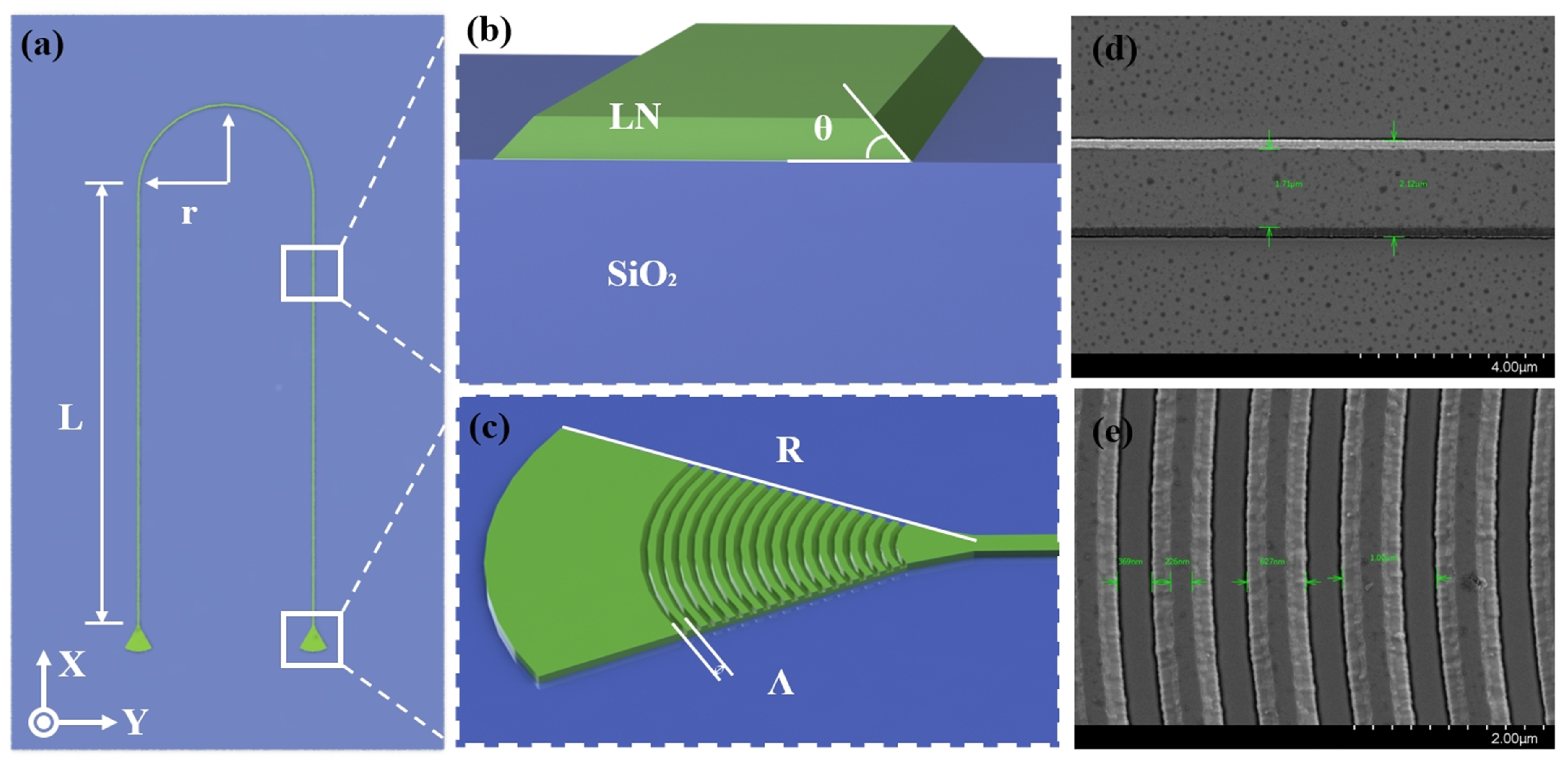
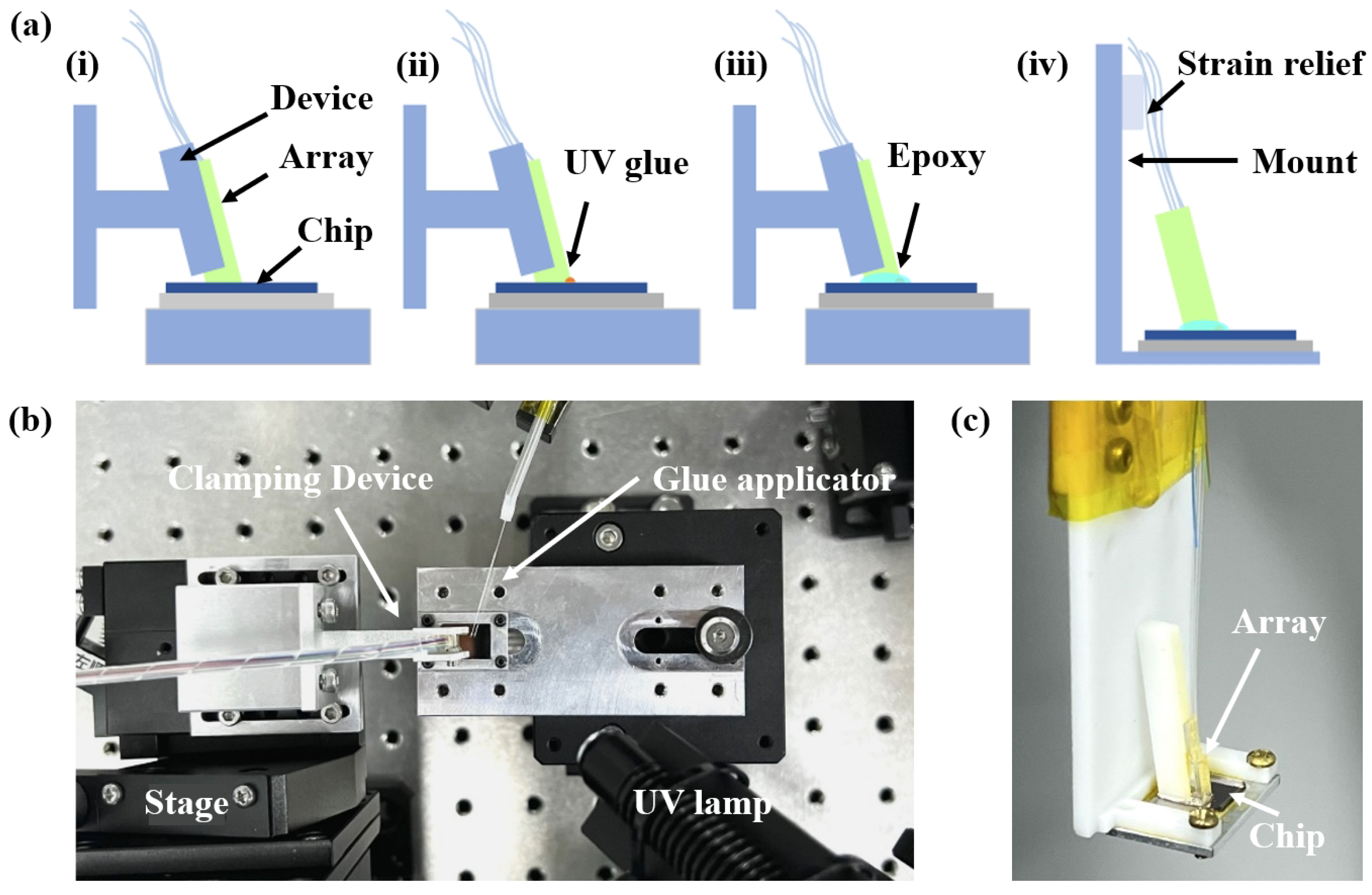
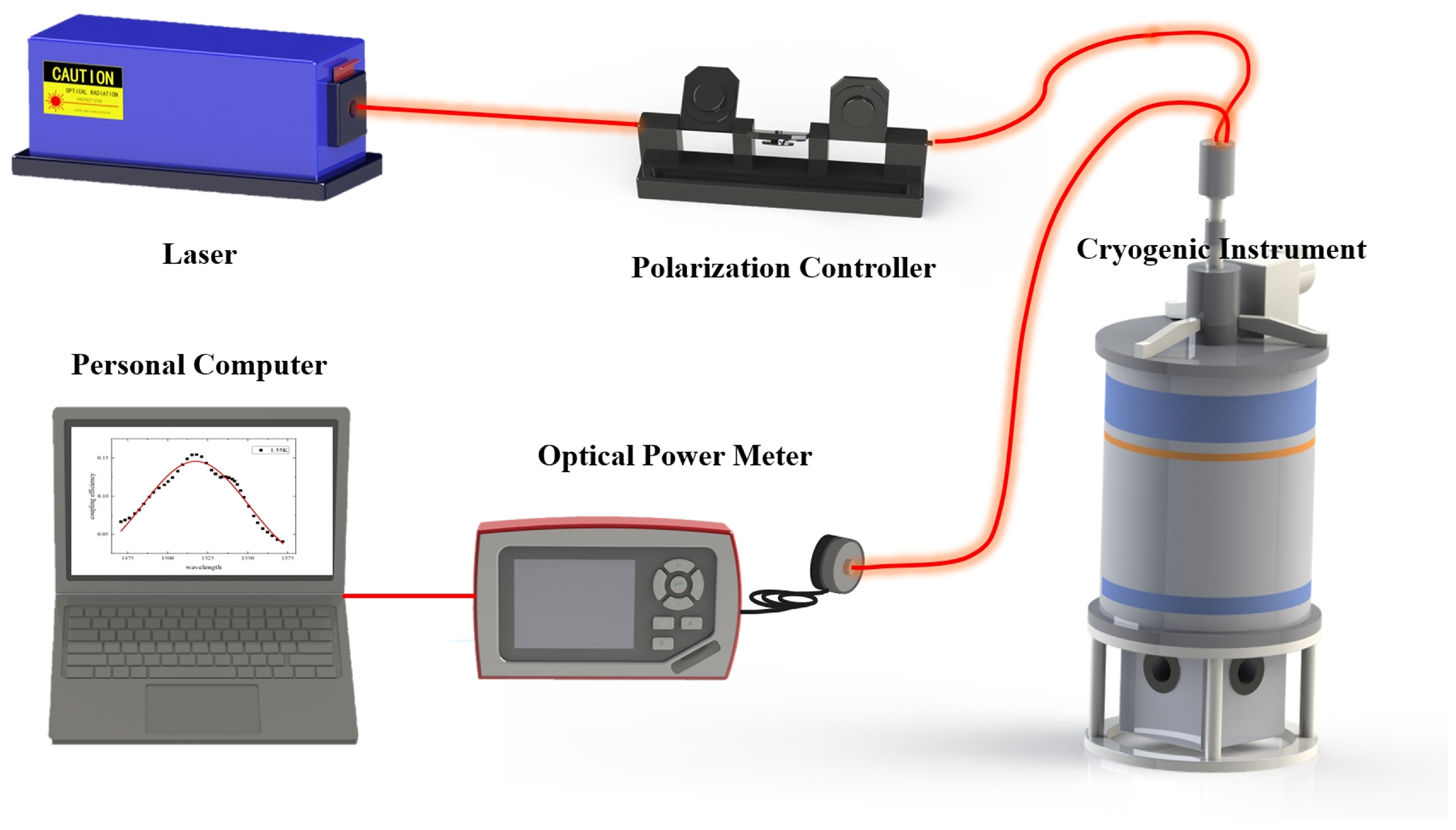
2. Fabrication and Packaging

A commercial z-cut LN film (NanoLN), 300 nm thick, is employed for the experiment. The light beam is coupled into the waveguide via a focusing grating coupler with a sector angle of 60°, a radius (R) of 31.5 μ m, a grating period (Λ) of 1 μ m, and a 50:50 duty cycle. The coupler includes 17 etched grooves with a depth of 140 nm (Figure 1). The waveguide is 2 μ m wide and 500 μ m long (L), with sidewalls inclined at an angle ( θ ) of 55.6°, as determined from scanning electron microscopic (SEM) images. A four-channel fiber array, tilted at 8° to reduce second-order reflections [36], is aligned with the grating couplers for signal input and output, with the couplers spaced 200 μ m apart to match the fiber array’s pitch (200 ± 1 μ m).
The commercial four-channel fiber array is bonded onto a 3D-printed resin base using a GE varnish and ethanol mixture to ensure stability and protection. The resin base is secured to the clamping device with set screws, which are subsequently mounted on a six-axis translation stage for precise alignment in the following steps.
The packaging process begins with the precise alignment of the fiber array to the target grating couplers, as illustrated in Figure 2(ai). This is followed by adjusting the X, Y, and Z position of the fiber array to maximize the optical power output, followed by fine-tuning of the polarization controller and the three angular degrees of freedom to achieve stable maximum transmission. Particular care is taken during Z-axis adjustments to avoid damaging the chip. Once alignment is achieved, a small drop of UV glue (NTT-AT6001, NTT Advanced Technology Corporation; Tokyo, Japan) is applied to one side of the fiber array to fix its position (Figure 2(aii)). The alignment is then reoptimized before curing the glue under UV light from different angles for five minutes. Following this pre-packaging step, a larger drop of two-part epoxy (EPO-TEK 301-2, Epoxy Technology; Billerica, MA, USA) is applied to the same side of the array (Figure 2(aiii)). The epoxy spreads via capillary action, encapsulating the array to provide full coverage and mechanical support. The assembly is left to cure at room temperature over 48 h. After curing, the packaged chip is detached and transferred to the mount prepared to be installed on the cryogenic sample rod (Figure 2(aiv)). To mitigate strain, we use double-sided tape and Kapton tape to secure the fiber away a few centimeters from the bottom of the fiber array.
The UV glue, noted for its rapid curing and high stability, enables precise initial alignment at room temperature. Pre-packaging with UV glue (Figure 2(aii)) effectively secures the alignment, minimizing efficiency losses during the prolonged curing of the two-part epoxy. However, UV glue is susceptible to cracking at low temperatures [27]. A cryogenic-compatible two-part epoxy provides robust mechanical support to address this limitation, ensuring the positional stability of the fiber array under cryogenic temperature conditions [34,37,38].

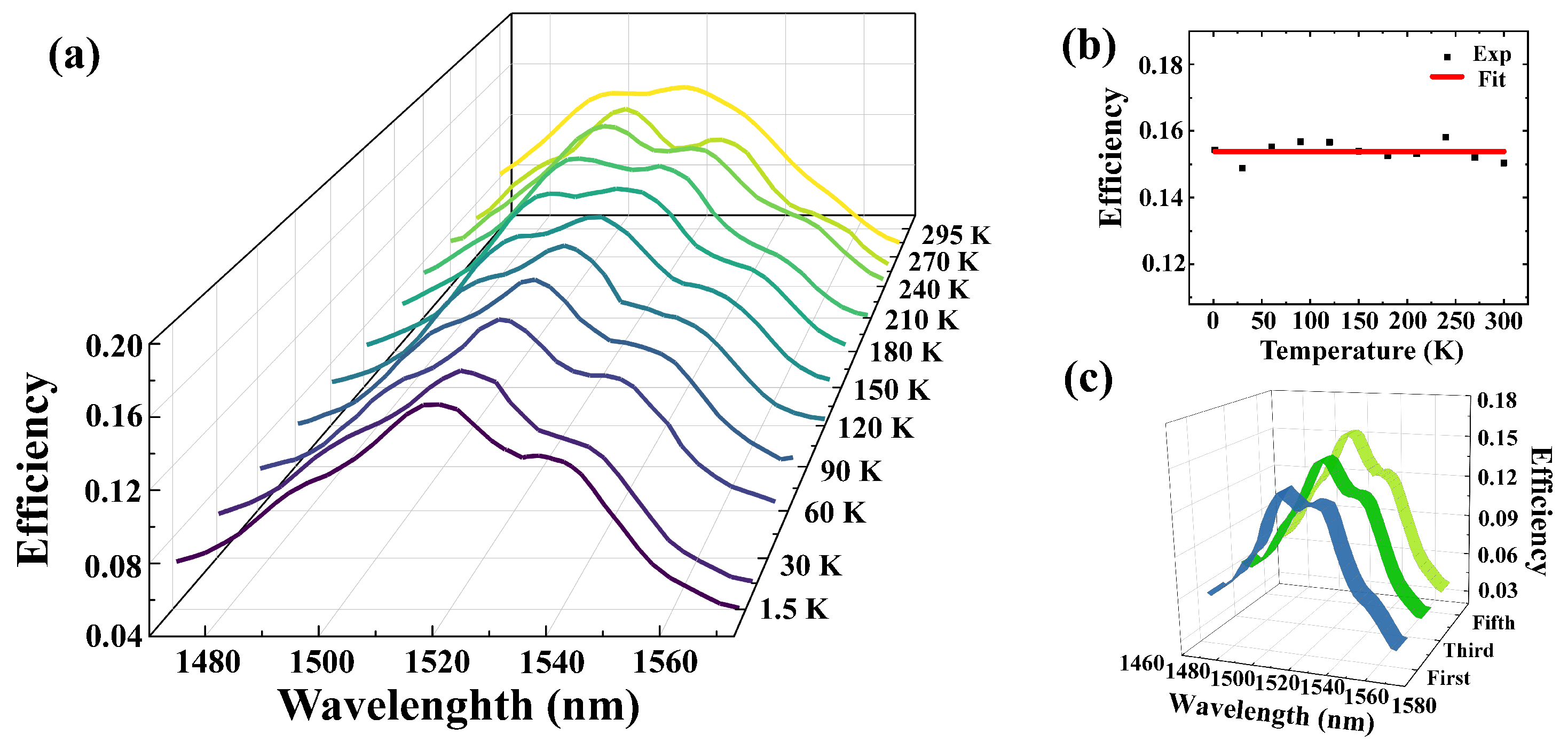
3. Experimental Results

The experimental setup for testing the cryogenic performance of the packaging is illustrated in Figure 3. A tunable diode laser (Toptica DLC Pro, Toptica, Munich, Germany), operating in the wavelength range of 1470–1570 nm, serves as the light source. The laser output is collected through an SMF-28 single-mode fiber, (Corning Incorporated, Corning, NY, USA) and directed through a polarization controller before being coupled into and out of the packaged chip. The input power before chip coupling is maintained at approximately 30 mW. The chip is securely mounted at the base of a cryogenic chamber (Oxford SpectromagPT system, Oxford Instruments NanoScience, Oxford, UK). The output signal is measured using an optical power meter (Thorlabs PM100D, Thorlabs, Newton, NJ, USA). By varying the laser wavelength and recording the optical power meter readout on a personal computer, the packaging efficiency as a function of wavelength could be obtained. Two chips were fabricated, packaged, and tested in this work.
At first, we compare the simulated and measured coupling efficiency of the grating coupler. The grating coupler for TE polarization was designed using 3D finite-difference time-domain simulations, and the simulated coupling efficiency is presented in Figure 4a. The coupling efficiency, F, is defined as follows: F = ( P o u t / P i n ) 1 / 2 . Here, P i n and P o u t denote the input and output power, respectively. To characterize the fabricated grating coupler, two grating couplers spaced 500 μ m apart and connected by a straight waveguide with 2 μ m width, as illustrated in Figure 4b. The coupling efficiency was measured using two angle-polished fibers [39]. The measured results, shown in Figure 4c, indicate a maximum coupling efficiency of 28.4% at 1526 nm. The measured results are lower than the simulated results, which we attribute to fabrication imperfections in the grating couplers and propagation losses in the waveguide.
After precise alignment of the fiber array (Figure 2(ai)), the measured coupling efficiency is 20.2% ± 3.5%. To investigate the coupling efficiency loss of the fiber array, we simulated the alignment tolerances of the fiber’s position (X/Y/Z axis) and angular [40]. Here, the X/Y axes present along/across the grating coupler, the Z axis is the distance between the fiber and grating coupler, the angular gives the aligned fiber angles in different directions (horizontal, vertical, and self-rotation). The simulated results indicate that the Z axis and angular misalignments exhibit relatively large alignment tolerances. Therefore, we primarily focus on the alignment tolerances along the X and Y axes. Figure 4d presents the simulated coupling efficiency as a function of X/Y displacement, showing a 1 dB loss penalty for a displacement of approximately ±1 μ m. Notably, fiber arrays may exhibit lower alignment tolerance compared to single fiber [41]. Therefore, the coupling efficiency loss in this step is mainly attributed to the pitch errors of the fiber array (200 ± 1 μ m).
Once the fiber array is precisely aligned, we proceed with the packaging process. The coupling efficiency is 17.0% ± 0.1% after applying and curing the UV glue (Figure 2(aii)), and 16.8% ± 1.2% after curing the two-part epoxy (Figure 2(aiii)). The overall coupling efficiency reduction of approximately 3.4% is mainly attributed to misalignment during the UV glue application and uneven curing. More delicate handling can minimize this loss, potentially maintaining the coupling efficiency at pre-packaging levels [33]. Following the packaging process, coupling efficiency further decreased to 15.7% ± 0.3% after mounting the chip onto the sample rod, mainly due to fiber bending. The packaged assembly was subsequently inserted into the cryogenic instrument and tested across a thermal cycle (1.5 K to 295 K).
We measured the packaging performance at different temperatures, with measurements taken at 30.0 K intervals (Figure 5a). As the temperature decreased, the transmission spectrum of the grating couplers remained stable, exhibiting a small blueshift of approximately 8 nm in the wavelength center. A statistical analysis of maximum coupling efficiencies at each temperature interval indicates consistent performance, with variations within ±0.5% relative to the mean maximum coupling efficiency of 15.4% (Figure 5b). To assess the robustness of the packaging, the same chip undergoes multiple thermal cycles. As shown in Figure 5c, the transmission spectrum shows high stability after one, three, and five thermal cycles.

4. Discussion and Conclusions

This paper details a cryogenic packaging method for TFLN photonic chips. The two selected types of glue have similar refractive indices (around 1.5) and exhibit well-matched thermal expansions behavior across varying temperatures. These properties enable a simplified packaging process and ensure stable performance, with a maximum coupling efficiency variation of only ±0.5% throughout the thermal cycle. Table 1 summarizes the packaging performance among different material platforms via grating couplers. While the coupling efficiency in this study is comparatively lower than in other works, it demonstrates excellent scalability and robust temperature-insensitive performance.
The coupling efficiency of the fiber array can be improved using the following strategies. First, the intrinsic coupling efficiency of the grating coupler can be improved by optimizing its design and refining fabrication precision [7,43]. Recent studies have demonstrated that incorporating reflection layers beneath the coupling grating and chirped grating couplers significantly enhances the coupling efficiency of the grating coupler, achieving an improvement of up to approximately 72.0% [43,44]. Second, the coupling efficiency losses due to array misalignment can be mitigated by employing fine-alignment arrays or more relaxed tolerances arrays, such as micro-lens arrays [45]. Additionally, the grating coupler’s polarization sensitivity remains a challenge in this study. To address this issue, a sub-wavelength grating structure can be employed to achieve a polarization-independent fiber-chip grating coupler [46]. Integrating these technologies is expected to enable high-efficiency, polarization-independent, and cryogenically compatible fiber-to-chip packaging.
In conclusion, this work introduces a temperature-insensitive packaging method for the fiber array to chip interface at cryogenic temperatures on the TFLN platform. The proposed fiber array can be integrated with a grating coupler array, facilitating chip-scale space-division multiplexing applications [47,48]. This robust and scalable method paves the way for the exploration of TFLN-based integrated devices operating at cryogenic temperatures, enabling applications such as microwave-to-photon conversion [14], quantum photon-pair generation [19], optical memory [49], and single-ion control and detection [42].

Author Contributions

Conceptualization and methodology, Y.W. and T.Y.; validation, Y.W., Y.M., X.W., and Z.Z.; formal analysis, Y.W.; data curation, Y.W., Y.M., X.W., and Z.Z.; writing—review and editing, Y.W. and T.Y.; supervision and project administration, Y.L. and T.Y. All authors have read and agreed to the published version of the manuscript.

Funding

This work was supported by the National Natural Science Foundation of China (62105321) and supported by the Fundamental Research Program of Shanxi Province (202403021211096).

Institutional Review Board Statement

Not applicable.

Informed Consent Statement

The study did not involve humans.

Data Availability Statement

The data underlying the results presented in this paper are not publicly available at this time but may be obtained from the authors upon reasonable request.

Conflicts of Interest

The authors declare no conflicts of interest.

References

  1. Zhu, D.; Shao, L.; Yu, M.; Cheng, R.; Desiatov, B.; Xin, C.; Hu, Y.; Holzgrafe, J.; Ghosh, S.; Shams-Ansari, A.; et al. Integrated photonics on thin-film lithium niobate. Adv. Opt. Photonics 2021, 13, 242–352. [Google Scholar] [CrossRef]
  2. Saravi, S.; Pertsch, T.; Setzpfandt, F. Lithium niobate on insulator: An emerging platform for integrated quantum photonics. Adv. Opt. Mater. 2021, 9, 2100789. [Google Scholar] [CrossRef]
  3. Smit, M.; Williams, K.; Van Der Tol, J. Past, present, and future of inp-based photonic integration. APL Photonics 2019, 4, 050901. [Google Scholar] [CrossRef]
  4. Wang, J.; Sciarrino, F.; Laing, A.; Thompson, M.G. Integrated photonic quantum technologies. Nat. Photonics 2020, 14, 273–284. [Google Scholar] [CrossRef]
  5. Ramakrishnan, R.K.; Ravichandran, A.B.; Mishra, A.; Kaushalram, A.; Hegde, G.; Talabattula, S.; Rohde, P.P. Integrated photonic platforms for quantum technology: A review. ISSS J. Micro Smart Syst. 2023, 12, 83–104. [Google Scholar] [CrossRef]
  6. Moody, G.; Chang, L.; Steiner, T.J.; Bowers, J.E. Chip-scale nonlinear photonics for quantum light generation. AVS Quantum Sci. 2020, 2, 041702. [Google Scholar] [CrossRef]
  7. Wu, R.; Wang, M.; Xu, J.; Qi, J.; Chu, W.; Fang, Z.; Zhang, J.; Zhou, J.; Qiao, L.; Chai, Z.; et al. Long low-loss-litium niobate on insulator waveguides with sub-nanometer surface roughness. Nanomaterials 2018, 8, 910. [Google Scholar] [CrossRef]
  8. Wang, C.; Zhang, M.; Chen, X.; Bertrand, M.; Shams-Ansari, A.; Chandrasekhar, S.; Winzer, P.; Lončar, M. Integrated lithium niobate electro-optic modulators operating at cmos-compatible voltages. Nature 2018, 562, 101–104. [Google Scholar] [CrossRef]
  9. Zhang, M.; Buscaino, B.; Wang, C.; Shams-Ansari, A.; Reimer, C.; Zhu, R.; Kahn, J.M.; Lončar, M. Broadband electro-optic frequency comb generation in a lithium niobate microring resonator. Nature 2019, 568, 373–377. [Google Scholar] [CrossRef]
  10. Fang, X.-X.; Du, H.-Y.; Zhang, X.; Wang, L.; Chen, F.; Lu, H. High-efficiency on-chip quantum photon source in modal phase-matched lithium niobate nanowaveguide. Laser Photonics Rev. 2025, 19, 2400782. [Google Scholar] [CrossRef]
  11. Wang, X.; Jiao, X.; Wang, B.; Liu, Y.; Xie, X.-P.; Zheng, M.-Y.; Zhang, Q.; Pan, J.-W. Quantum frequency conversion and single-photon detection with lithium niobate nanophotonic chips. npj Quantum Inf. 2023, 9, 38. [Google Scholar] [CrossRef]
  12. Feng, H.; Ge, T.; Guo, X.; Wang, B.; Zhang, Y.; Chen, Z.; Zhu, S.; Zhang, K.; Sun, W.; Huang, C.; et al. Integrated lithium niobate microwave photonic processing engine. Nature 2024, 627, 80–87. [Google Scholar] [CrossRef] [PubMed]
  13. Youssefi, A.; Shomroni, I.; Joshi, Y.J.; Bernier, N.R.; Lukashchuk, A.; Uhrich, P.; Qiu, L.; Kippenberg, T.J. A cryogenic electro-optic interconnect for superconducting devices. Nat. Electron. 2021, 4, 326–332. [Google Scholar] [CrossRef]
  14. Shen, M.; Xie, J.; Xu, Y.; Wang, S.; Cheng, R.; Fu, W.; Zhou, Y.; Tang, H.X. Photonic link from single-flux-quantum circuits to room temperature. Nat. Photonics 2024, 18, 371–378. [Google Scholar] [CrossRef]
  15. Lomonte, E.; Wolff, M.A.; Beutel, F.; Ferrari, S.; Schuck, C.; Pernice, W.H.; Lenzini, F. Single-photon detection and cryogenic reconfigurability in lithium niobate nanophotonic circuits. Nat. Commun. 2021, 12, 6847. [Google Scholar] [CrossRef]
  16. Mobassem, S.; Lambert, N.J.; Rueda, A.; Fink, J.M.; Leuchs, G.; Schwefel, H.G. Thermal noise in electro-optic devices at cryogenic temperatures. Quantum Sci. Technol. 2021, 6, 045005. [Google Scholar] [CrossRef]
  17. Riedinger, R.; Wallucks, A.; Marinković, I.; Löschnauer, C.; Aspelmeyer, M.; Hong, S.; Gröblacher, S. Remote quantum entanglement between two micromechanical oscillators. Nature 2018, 556, 473–477. [Google Scholar] [CrossRef]
  18. Zhao, M.; Fang, K. Observation of photon-phonon correlations via dissipative filtering. Phys. Rev. Appl. 2022, 18, 034043. [Google Scholar] [CrossRef]
  19. Cheng, Y.; Li, X.; Feng, L.; Li, H.; Sun, W.; Song, X.; Ding, Y.; Guo, G.; Wang, C.; Ren, X. Efficient cryogenic nonlinear conversion processes in periodically-poled thin-film lithium niobate waveguides. Laser Photonics Rev. 2025, 19, 2401491. [Google Scholar] [CrossRef]
  20. Sund, P.I.; Lomonte, E.; Paesani, S.; Wang, Y.; Carolan, J.; Bart, N.; Wieck, A.D.; Ludwig, A.; Midolo, L.; Pernice, W.H.; et al. High-speed thin-film lithium niobate quantum processor driven by a solid-state quantum emitter. Sci. Adv. 2023, 9, eadg7268. [Google Scholar] [CrossRef]
  21. Cohen, J.D.; Meenehan, S.M.; MacCabe, G.S.; Gröblacher, S.; Safavi-Naeini, A.H.; Marsili, F.; Shaw, M.D.; Painter, O. Phonon counting and intensity interferometry of a nanomechanical resonator. Nature 2015, 520, 522–525. [Google Scholar] [CrossRef] [PubMed]
  22. McKenna, T.P.; Patel, R.N.; Witmer, J.D.; Laer, R.V.; Valery, J.A.; Safavi-Naeini, A.H. Cryogenic packaging of an optomechanical crystal. Opt. Express 2019, 27, 28782–28791. [Google Scholar] [CrossRef] [PubMed]
  23. Wasserman, W.; Harrison, R.; Harris, G.; Sawadsky, A.; Sfendla, Y.; Bowen, W.; Baker, C. Cryogenic and hermetically sealed packaging of photonic chips for optomechanics. Opt. Express 2022, 30, 30822–30831. [Google Scholar] [CrossRef]
  24. Vermeulen, D.; Poulton, C.V. Optical interfaces for silicon photonic circuits. Proc. IEEE 2018, 106, 2270–2280. [Google Scholar] [CrossRef]
  25. Carroll, L.; Lee, J.-S.; Scarcella, C.; Gradkowski, K.; Duperron, M.; Lu, H.; Zhao, Y.; Eason, C.; Morrissey, P.; Rensing, M.; et al. Photonic packaging: Transforming silicon photonic integrated circuits into photonic devices. Appl. Sci. 2016, 6, 426. [Google Scholar] [CrossRef]
  26. Zeng, B.; De-Eknamkul, C.; Assumpcao, D.; Renaud, D.; Wang, Z.; Riedel, D.; Ha, J.; Robens, C.; Levonian, D.; Lukin, M.; et al. Cryogenic packaging of nanophotonic devices with a low coupling loss < 1 db. Appl. Phys. Lett. 2023, 123, 161106. [Google Scholar]
  27. Lin, B.; Witt, D.; Young, J.F.; Chrostowski, L. Cryogenic optical packaging using photonic wire bonds. APL Photonics 2023, 8, 126109. [Google Scholar] [CrossRef]
  28. Chen, G.; Chen, K.; Yu, Z.; Liu, L. Low-loss and broadband polarization-diversity edge coupler on a thin-film lithium niobate platform. Opt. Lett. 2023, 48, 4145–4148. [Google Scholar] [CrossRef]
  29. Chen, B.; Ruan, Z.; Wang, M.; Gong, S.; Liu, L. High-performance and fabrication-tolerant edge coupler on thin film lithium niobate based on a three-dimensional inverse taper. APL Photonics 2024, 9, 116111. [Google Scholar] [CrossRef]
  30. Chen, S.; Ourari, S.; Raha, M.; Phenicie, C.M.; Uysal, M.T.; Thompson, J.D. Hybrid microwave-optical scanning probe for addressing solid-state spins in nanophotonic cavities. Opt. Express 2021, 29, 4902–4911. [Google Scholar] [CrossRef]
  31. Chen, B.; Ruan, Z.; Fan, X.; Wang, Z.; Liu, J.; Li, C.; Chen, K.; Liu, L. Low-loss fiber grating coupler on thin film lithium niobate platform. APL Photonics 2022, 7, 076103. [Google Scholar] [CrossRef]
  32. Lomonte, E.; Lenzini, F.; Pernice, W.H. Efficient self-imaging grating couplers on a lithium-niobate-on-insulator platform at near-visible and telecom wavelengths. Opt. Express 2021, 29, 20205–20216. [Google Scholar] [CrossRef] [PubMed]
  33. You, M.; Lin, Z.; Li, X.; Liu, J. Chip-scale silicon ring resonators for cryogenic temperature sensing. J. Light. Technol. 2020, 38, 5768–5773. [Google Scholar] [CrossRef]
  34. Witt, D.; Chrostowski, L.; Young, J. Packaged cryogenic photon pair source using an effective packaging methodology for cryogenic integrated optics. arXiv 2024, arXiv:2401.02068. [Google Scholar]
  35. Ranno, L.; Gupta, P.; Gradkowski, K.; Bernson, R.; Weninger, D.; Serna, S.; Agarwal, A.M.; Kimerling, L.C.; Hu, J.; Brien, P.O. Integrated photonics packaging: Challenges and opportunities. ACS Photonics 2022, 9, 3467–3485. [Google Scholar] [CrossRef]
  36. Zhang, C.; Sun, J.-H.; Xiao, X.; Sun, W.-M.; Zhang, X.-J.; Chu, T.; Yu, J.-Z.; Yu, Y.-D. High efficiency grating coupler for coupling between single-mode fiber and soi waveguides. Chin. Phys. Lett. 2013, 30, 014207. [Google Scholar] [CrossRef]
  37. Mehta, K.K.; Zhang, C.; Malinowski, M.; Nguyen, T.-L.; Stadler, M.; Home, J.P. Integrated optical multi-ion quantum logic. Nature 2020, 586, 533–537. [Google Scholar] [CrossRef]
  38. Starling, D.J.; Shtyrkova, K.; Christen, I.; Murphy, R.; Li, L.; Chen, K.C.; Kharas, D.; Zhang, X.; Cummings, J.; Nowak, W.J.; et al. Fully packaged multichannel cryogenic quantum memory module. Phys. Rev. Appl. 2023, 19, 064028. [Google Scholar] [CrossRef]
  39. Snyder, B.; O’Brien, P. Packaging process for grating-coupled silicon photonic waveguides using angle-polished fibers. IEEE Trans. Components Packag. Manuf. Technol. 2013, 3, 954–959. [Google Scholar] [CrossRef]
  40. Li, C.; Chee, K.S.; Tao, J.; Zhang, H.; Yu, M.; Lo, G.Q. Silicon photonics packaging with lateral fiber coupling to apodized grating coupler embedded circuit. Opt. Express 2014, 22, 24235–24240. [Google Scholar] [CrossRef]
  41. Zimmermann, L.; Preve, G.B.; Tekin, T.; Rosin, T.; Landles, K. Packaging and assembly for integrated photonics—A review of the epixpack photonics packaging platform. IEEE J. Sel. Top. Quantum Electron. 2011, 17, 645–651. [Google Scholar] [CrossRef]
  42. Yang, L.; Wang, S.; Shen, M.; Xie, J.; Tang, H.X. Controlling single rare earth ion emission in an electro-optical nanocavity. Nat. Commun. 2023, 14, 1718. [Google Scholar] [CrossRef] [PubMed]
  43. Kang, S.; Zhang, R.; Hao, Z.; Jia, D.; Gao, F.; Bo, F.; Zhang, G.; Xu, J. High-efficiency chirped grating couplers on lithium niobate on insulator. Opt. Lett. 2020, 45, 6651–6654. [Google Scholar] [CrossRef]
  44. Krasnokutska, I.; Chapman, R.J.; Tambasco, J.-L.J.; Peruzzo, A. High coupling efficiency grating couplers on lithium niobate on insulator. Opt. Express 2019, 27, 17681–17685. [Google Scholar] [CrossRef]
  45. Scarcella, C.; Gradkowski, K.; Carroll, L.; Lee, J.-S.; Duperron, M.; Fowler, D.; O’Brien, P. Pluggable single-mode fiber-array-to-pic coupling using micro-lenses. IEEE Photonics Technol. Lett. 2017, 29, 1943–1946. [Google Scholar] [CrossRef]
  46. Chen, B.; Ruan, Z.; Chen, K.; Liu, L. One-dimensional grating coupler on lithium-niobate-on-insulator for high-efficiency and polarization-independent coupling. Opt. Lett. 2023, 48, 1434–1437. [Google Scholar] [CrossRef]
  47. Ding, Y.; Ye, F.; Peucheret, C.; Ou, H.; Miyamoto, Y.; Morioka, T. On-chip grating coupler array on the soi platform for fan-in/fan-out of mcfs with low insertion loss and crosstalk. Opt. Express 2015, 3, 3292–3298. [Google Scholar] [CrossRef]
  48. Luo, H.; Chen, L.; Yu, S.; Cai, X. Efficient four-way vertical coupler array for chip-scale space-division-multiplexing applications. Opt. Lett. 2021, 46, 4324–4327. [Google Scholar] [CrossRef]
  49. Dutta, S.; Zhao, Y.; Saha, U.; Farfurnik, D.; Goldschmidt, E.A.; Waks, E. An atomic frequency comb memory in rare-earth-doped thin-film lithium niobate. ACS Photonics 2023, 10, 1104–1109. [Google Scholar] [CrossRef]
Figure 1. (a) Schematic of the fabricated chip layout. (b,c) Magnified views of the region enclosed by solid lines in (a), showing detailed structures of the waveguide and grating coupler. (d,e) SEM images corresponding to the regions in (b) and (c), respectively.
Photonics 12 00545 g001
Figure 2. (a) Schematic of the packaging process: (i) The precise alignment of the fiber array to the target grating couplers. (ii) Apply a small drop of UV glue to one side of the fiber array. (iii) Cover the bottom of the fiber array completely with a large drop of two-part epoxy. (iv) Transfer the packaged chip to the mount prepared for installation on the cryogenic sample rod. (b) Photograph of the packaging setup. A spare SMF-28 fiber fixed on a three-axis stage is used as a glue applicator. (c) Photograph of the packaged chip, which has been transferred to the mount prepared to be installed on the cryogenic sample rod.
Photonics 12 00545 g002
Figure 3. Schematic diagram of the experimental setup.
Photonics 12 00545 g003
Figure 4. (a) Simulated coupling efficiency of the grating coupler. (b) Optical microscope image showing two grating couplers connected by a straight waveguide (upper image). Two angle-polished fibers were used to measure the coupling efficiency (lower image). (c) Measured coupling efficiency corresponding to the setup in (b). (d) Simulated coupling efficiency as a function of fiber X/Y misalignment.
Photonics 12 00545 g004
Figure 5. (a) Packaging performance of the chip across the telecom band from 1.5 K to 295 K. (b) Variation in maximum coupling efficiency of the chip during thermal cycling. The black dots represent the maximum coupling efficiency at each temperature interval, while the red line indicates the mean maximum coupling efficiency. (c) Wavelength-efficiency curves of a single chip at 1.5 K after one, three, and five thermal cycles.
Photonics 12 00545 g005
Table 1. A comparative analysis of packaging performance using grating couplers on different platforms and the associated coupling efficiency losses at cryogenic temperatures (CEL-Cryo).
PlatformReferenceScalabilityMethodTemperature/EfficiencyCEL-Cryo
Si[22]Single fiberUV Glue7 mK/∼20%∼8%
[33]Fiber arrayUV Glue180 K/∼0.3%∼20%
[34]Fiber arrayEpoxy5 K/∼38%∼4%
TFLN[14]Single fiberUV Glue4 K/∼25%
[42]Single fiberUV Glue1 K/∼10%
This workFiber arrayUV Glue + Epoxy1.5 K/∼15.7%∼0.5%
Disclaimer/Publisher’s Note: The statements, opinions and data contained in all publications are solely those of the individual author(s) and contributor(s) and not of MDPI and/or the editor(s). MDPI and/or the editor(s) disclaim responsibility for any injury to people or property resulting from any ideas, methods, instructions or products referred to in the content.

