Abstract
Compared with conventional detectors, a circularly polarized detector operating at 4.26 μm effectively suppresses background noise (e.g., solar scattering and atmospheric interference), enabling high-precision CO2 monitoring across ecosystems like farmland, forests, and wetlands. This capability allows the precise quantification of carbon sink potential and ecosystem health. Our design employs a mid-wave HgCdTe detector—a well-established platform—combined with a CMOS-compatible Si/SiO2 metasurface. Geometric displacements were applied to break C2 symmetry, achieving a chiral design. Through multiparameter optimization, we realized a circularly polarized photodetector (CPPD) with a CPER of 18 dB, expected to demonstrate superior CO2 monitoring performance. These advances may offer researchers and practitioners a robust tool for both fundamental studies and field deployments.
1. Introduction
Carbon dioxide (CO2) [1], a primary greenhouse gas, contributes directly to global warming through its increasing atmospheric concentration [2]. This phenomenon drives climate change impacts including extreme weather events, sea level rise, and ecosystem disruption [3]. Infrared photodetectors operating at 4.26 μm—corresponding to CO2’s strong absorption peak—provide unparalleled capabilities for high-precision gas detection and environmental monitoring. However, conventional intensity-based detectors suffer significant limitations. They are particularly vulnerable to background noise sources like sunlight scattering and atmospheric interference, which degrade signal-to-noise ratios and compromise measurement accuracy in complex environments [4]. Furthermore, atmospheric turbulence and multiple scattering effects impair signal stability, restricting their effectiveness for long-range monitoring applications [5]. In comparison, circularly polarized infrared detectors [6,7,8] demonstrate superior performance characteristics. They overcome the inherent limitations of conventional detectors by offering enhanced measurement accuracy, improved noise immunity, and greater signal stability—essential attributes for meeting the rigorous demands of modern environmental monitoring and scientific research.
Early implementations of circularly polarized infrared detectors relied on optical systems incorporating quarter-wave plates [9,10] and 45° linear polarizers [11,12]. However, these systems were plagued by bulky form factors and substantial mechanical noise. The emergence of metasurface technology has effectively overcome these limitations. Metasurfaces [13,14,15,16,17] provide numerous advantages including ultrathin and lightweight profiles, high design flexibility, broadband operational capability, planar integration compatibility, multifunctional performance, precise light field manipulation, environmental robustness, and cost-effective fabrication. Recently, based on circular dichroism [18,19,20,21,22] metasurfaces, some excellent circular polarization detectors have been gradually reported. In 2020, Wang et al. [23] developed a chip-scale polarimeter integrating four graphene–silicon photodetectors capable of extracting full Stokes parameters through inter-detector information processing. In 2023, Yang et al. [24] developed a mid-infrared circularly polarized photodetector using asymmetric silicon gratings, achieving 0.7 circular dichroism absorption at λ = 8.163 µm. In 2023, Yao et al. [25] implemented a metasurface-based full-Stokes imaging sensor by integrating a polarization filter array with CMOS technology, enabling single-shot polarization imaging with a 40° field of view and dual-color operation. In 2024, Chen et al. [26] created an on-chip full-Stokes polarimeter using four plasmonic metasurface subpixels, achieving < 1% root mean square error in full polarization reconstruction via machine learning algorithms. In 2025, Zhu et al. [27] demonstrated a detector combining helical nanostructures with perovskite photodiodes, achieving a remarkable photocurrent anisotropy factor of 1.96 at visible wavelengths for quantitative polarization state analysis.
In this work, we investigate the integration of chiral metasurfaces with commercial HgCdTe detectors [28,29] to optimize performance while maintaining fabrication simplicity. A circularly polarized photodetector (CPPD) was developed by vertically stacking a HgCdTe detection layer with a chiral silicon metasurface. The metasurface’s unit cells break chiral symmetry to enable polarization selectivity. Under right-circularly polarized (RCP) illumination, counter-rotating current loops are generated, inducing destructive interference that blocks RCP transmission. Using COMSOL Multiphysics simulations, we quantified the performance sensitivity to fabrication tolerances.
2. Materials and Methods
Figure 1a illustrates the three-dimensional structure of the CPPD, which consists of a HgCdTe detector at the bottom and a silicon metasurface on top. The HgCdTe detector, also referred to as the MCT detector, converts incident photons into electrons collected by electrodes but lacks intrinsic polarization selectivity. The unit cell of the silicon metasurface exhibits a typical chiral symmetric structure, enabling significantly higher transmission for left-circularly polarized (LCP) light compared with RCP. Figure 1b provides the xz cross-sectional view of the CPPD, detailing its structural specifics and material composition. Figure 1c shows the xy cross-sectional view of the silicon metasurface in the CPPD, while Figure 1d presents the mirror image of Figure 1c about the YZ plane, indicating the opposite circular polarization selection characteristics compared with Figure 1a, favoring RCP transmission. The incident light propagates along the negative Z-axis. The absorption properties of optical materials are typically quantified by the optical absorption length, = , where denotes the distance over which the light intensity decays to 1/e, represents the imaginary part of the refractive index, and is the wavelength in free space. Clearly, smaller values of correspond to larger , implying weaker absorption characteristics. Figure 1e displays the optical refractive indices of SiO2 and MCT, with real parts of approximately 1.398 and 3.447, respectively. As shown in Figure 1f, the blue circle represents the of SiO2, which is the actual value reduced by a factor of one million. At the operating wavelength of 4.26 μm, the blue circle overlaps with the red line representing MCT’s absorption characteristics near an of 2.1 μm. Figure 1g outlines the COMSOL model used to simulate the optical properties of the CPPD. Periodic boundary conditions, commonly employed in photonic crystals and antenna arrays, confine the electromagnetic fields in the X and Y directions. Perfectly matched layers (PMLs), utilized to simulate infinite-space electromagnetic wave propagation, are placed at the top and bottom of the model to absorb outgoing waves. The maximum mesh sizes for MCT and silicon are set to 90 nm and 50 nm, respectively, and the PMLs comprise 30 layers to ensure rapid field decay within the layer. The device’s transmission and reflection rates are determined by integrating the Poynting vector over the inner boundaries of the PMLs, and the CPPD’s absorption rate is obtained by subtracting these rates from unity. In addition, the circularly polarized MCT can be prepared through the following steps: After the processing of the HgCdTe device is completed, the surface is cleaned first. Then, a layer of SiO2 is grown on the ZnS passivation layer by PECVD. Subsequently, a silicon layer is deposited on the SiO2 surface using low-temperature sputtering or PECVD. The passivation layer and low-temperature conditions can effectively prevent thermal damage to the MCT detector during the process. After that, the patterning of the metasurface is completed through electron beam lithography and inductively coupled plasma etching. Selective etching gas and etching endpoint detection technology can effectively avoid over-etching problems. Throughout the process, due to the poor thermal stability of HgCdTe, all processes are preferably completed at low temperatures (<200 °C), with priority given to ALD, low-temperature PECVD, and sputtering. Thermal treatment is also conducted using local heating (such as laser annealing) instead of global thermal treatment.
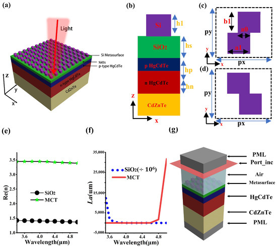
Figure 1.
Structure and material information of the circularly polarized photodetector. The composition of mercury cadmium telluride is Hg0.68Cd0.32Te. (a): Three-dimensional structure of the CPPD. (b): XZ cross-sectional view of the circularly polarized detector. h1 = 0.98 μm, hs = 3 μm, hp = 2.5 μm, hn = 7.5 μm. (c,d): XY cross-sectional view of the silicon metasurface in the circularly polarized detector and its mirror image about the YZ plane. px = 2.4 μm, py = 2.4 μm, a0 = 0.4 μm, a1 = 0.97 μm, b1 = 0.92 μm. (e): Optical refractive indices of the absorbing materials in SiO2 and MCT. (f): The optical absorption length of the material. (g): Schematic diagram of the COMSOL simulation model for calculating optical parameters.
3. Results
Figure 2a illustrates the absorption spectrum and CPER spectrum of CPPD in the 4.0–4.5 μm wavelength range. Here, CPER is defined as , where and represent the absorption rates of CPPD for LCP and RCP, respectively. For LCP, the absorption rate initially increases with wavelength and then decreases, reaching a peak value of 0.82 at 4.27 μm. For RCP, the minimum absorption rate occurs at the operating wavelength of 4.26 μm, indicating that CPPD does not respond to RCP. The inset in Figure 2a depicts the 2D structural diagram of a conventional MCT detector. Since no filter is present on its top, it inherently lacks sensitivity to the polarization information of incident light. The light blue dots and dark blue solid line represent the absorption rates of the 2D MCT chip for RCP and LCP, respectively. These two curves exhibit complete overlap as expected. The red five-pointed star represents the CPER spectrum of CPPD, with a maximum value of 18 dB corresponding to the minimum absorption rate of RCP. Furthermore, it is observed that at the operating wavelength of 4.26 μm, the absorption rate of CPPD for LCP is lower than that of the 2D MCT chip. This suggests that while the silicon chiral metasurface enhances the ability to detect circularly polarized signals in spatial light, this advantage comes at the cost of reduced device efficiency. Therefore, this high-performance CPPD may be more suitable for applications requiring sensitivity to circularly polarized signals, such as quantum communication and quantum computing, atmospheric detection, and display technology and augmented reality. Given that the maximum CD value and the maximum CPER do not coincide at the same operating wavelength in Figure 2a, a more comprehensive performance metric for evaluating CPPD should be introduced. CPQF is a new metric resulting from the combined effects of CD and CPER, expressed as CPQF = CD × CPER, where CD = − . Figure 2b shows the CPQF spectrum of CPPD, with its maximum value occurring at an operating wavelength of 4.26 μm, providing evidence of its potential application in CO2 monitoring.
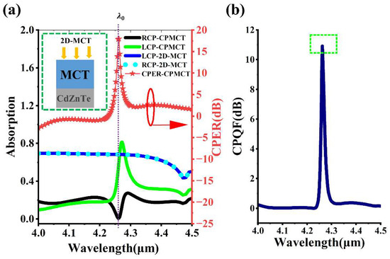
Figure 2.
Absorption spectrum, CPER spectrum, and CPQF spectrum. (a): The absorption spectra of CPMCT and 2D-MCT and the CPER spectrum of CPMCT. (b): CPQF spectrum of CPMCT.
3.1. Investigation into the Origin of Chirality in Silicon Metasurfaces
In fact, the circular dichroism of CPPD can be attributed to the chirality exhibited by the silicon metasurface in the transmission space. For LCP, the silicon metasurface allows some photons to pass through the SiO2 layer and enter the MCT device, where they are converted into photoelectrons that can subsequently be collected by the electrodes. In contrast, for RCP, the silicon metasurface behaves as a near-perfect reflector, with almost no photons transmitted into the region below. Typically, the chiral symmetry of the metasurface’s unit cell determines its CD characteristics. Here, chiral symmetry refers to a geometric structure that cannot be fully superimposed onto its mirror image via any combination of rotation or translation operations. Figure 3a illustrates the chiral evolution of the metasurface unit cell. The basic structure consists of two identical rectangles, with the upper rectangle highlighted by an orange border for clarity. As the upper rectangle shifts to the right, the unit cell transitions from a C2 symmetric configuration to a chiral symmetric one. Figure 3b is primarily used to quantitatively evaluate the impact of the dislocation length Δx on the CD of the silicon metasurface. Specifically, , where and denote the transmission rates of the silicon metasurface for LCP and RCP, respectively. When Δx equals 0 nm, corresponding to a C2 symmetric unit cell, the metasurface lacks chiral symmetry, resulting in zero CD across all wavelengths. As Δx increases, the CD peak exhibits a gradual redshift, with the peak intensity initially increasing and then decreasing. As evident in Figure 3b, there exists a strong correlation between the chiral symmetric structure and the observed CD. Furthermore, the alignment and bonding between the silicon metasurface and MCT typically rely on three processes: indium pillar alignment or glass via technology, dielectric support layers, and organic adhesive bonding. Under these processes, the medium between the silicon metasurface and MCT is generally air, dielectrics (such as silicon dioxide or silicon nitride), or epoxy resin. Figure 3c depicts the variation in CD of the silicon metasurface under different alignment processes, with the highest CD achieved using the dielectric support layer process, where SiO2 serves as the dielectric material. Figure 3d presents the transmission spectrum and CPER spectrum of the silicon metasurface. Here, CPER is defined as 10 × log (/), where and represent the transmission rates of the silicon metasurface for LCP and RCP, respectively. The minimum transmission rate for RCP occurs at an operating wavelength of 4.26 μm, corresponding to a maximum CPER value of 23.5 dB.
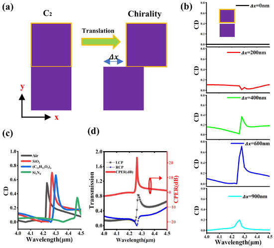
Figure 3.
Transmission characteristics of silicon metasurfaces. (a): Dislocation length Δx. (b): CD spectra under different dislocation lengths. (c): CD spectra under different alignments of the metasurface and the detector. The molecular formula of epoxy resin is (C11H12O3)n. (d): Transmission spectra and CPER spectra of the silicon metasurface.
For metasurfaces, near-field distribution maps are of critical importance [9,30]. These maps can not only reveal the localization characteristics and coupling effects of electromagnetic fields but also provide insights into the electromagnetic response mechanisms and energy dissipation processes. Figure 4 presents the electric field intensity distribution map and equivalent current vector direction map of the silicon metasurface in the xy cross-section. The labels 1/4, 1/2, and 3/4 above the figure correspond to the Z-axis positions at 1/4, 1/2, and 3/4 of the metasurface height, respectively. The six electric field intensity distribution maps share a common color scale, with the equivalent currents corresponding to LCP and RCP represented by black and red arrows, respectively. The thickness of the arrows indicating the equivalent current in the silicon metasurface is proportional to the current intensity. For LCP, the electric field is concentrated not only along the boundaries of the rectangle but also significantly localized at points 1 and 2. The equivalent currents at the three cross-sections of the silicon metasurface are relatively weak and can be neglected. In contrast, for RCP, the electric field localization is much weaker compared with the LCP case and is primarily confined to the interface between the rectangle and air. The intensity of the equivalent current indicated by the red arrows is substantial and cannot be ignored. The equivalent current rotates counterclockwise within the upper rectangle and clockwise within the lower rectangle. Based on the theory outlined in Reference [28], it is hypothesized that the superposition of the light wave generated by the point-source resonance (indicated by the red arrow) and the right-circularly polarized (RCP) wave at the transmission end results in a typical coherent destructive interference phenomenon in optics. This elucidates why almost no photon energy leaks into the underlying silica material.
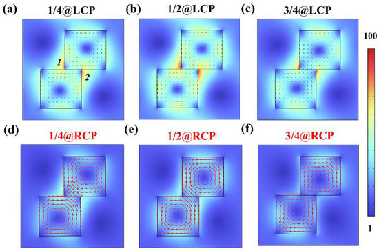
Figure 4.
Near-field electric field intensity map and equivalent current vector map of the silicon metasurface at the operating wavelength of 4.26 μm. The symbols “1/4”, “1/2” and “3/4” in the subfigure correspond respectively to the cases where the XY cross-section is located at 1/4, 1/2 and 3/4 of the height of the metasurface. The black arrows and red arrows respectively correspond to the equivalent current directions of LCP and RCP. The thickness of the arrows is proportional to the intensity of the current.
3.2. Optimization of the Dielectric Support Layer Thickness (hs) in CPPD
In optics, when two metasurfaces are brought into close proximity or integrated, their interaction can lead to a range of optical phenomena, including Fabry–Perot resonance, mode coupling and hybridization, near-field coupling and energy transfer, as well as non-reciprocal transmission. However, in the case of the CPPD depicted in Figure 1a, the upper silicon metasurface and the lower MCT detector must function as independent optical components. Consequently, it is crucial to investigate how the thickness hs of the intermediate medium layer affects the performance of the CPPD. Figure 5a illustrates the impact of the SiO2 spacer layer thickness hs on the absorption rate and CPER of the CPPD. As hs increases, the absorption rate of RCP initially decreases sharply before gradually tapering off, remaining relatively constant for hs > 2.7 μm. In contrast, the absorption rate of LCP exhibits irregular peaks and valleys, with maximum and minimum peak values of approximately 0.81 and 0.27, respectively. Furthermore, the CPER also displays multiple peaks, though its largest peak does not align with the design wavelength of 4.26 μm. To determine the optimal hs, CPQF appears to take precedence over absorption rate and CPER. As indicated by the red circle in Figure 5b, the CPPD achieves its highest CPQF peak at hs = 3 μm.
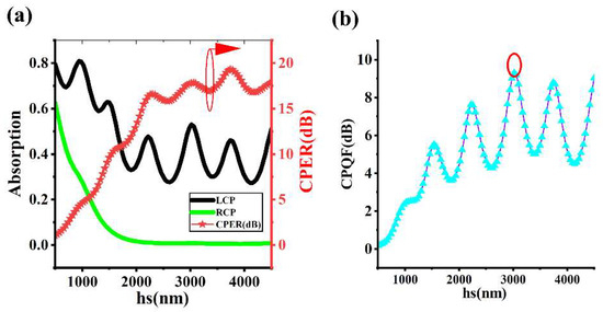
Figure 5.
The influence of the dielectric support layer thickness hs of CPPD on absorption, CPER, and CPQF. (a): The influence of the hs on the absorption and CPER of CPMCT. (b): The impact of the hs on the CPQF of CPMCT. The red circle corresponds to the optimal hs.
3.3. Analysis of Potential Process Errors
In the preceding chapters, we analyzed the origin of circular dichroism in silicon metasurfaces and the influence of the spacer thickness hs on the performance of CPPD. In this chapter, we primarily employ COMSOL 5.6 software to evaluate the extent of performance degradation in CPPD caused by potential fabrication errors introduced during the manufacturing process. As shown in Figure 6a, factors such as optical diffraction effects, the chemical properties of photoresist, or anisotropy during etching can cause the vertices of the rectangular structure to become rounded corners with a radius of r0. Figure 6b demonstrates that when r0 is less than 100 nm, the absorption rate of RCP remains nearly constant, whereas that of LCP exhibits a gradual increase. Figure 6c,e illustrate the processing errors Δh associated with under-etching and over-etching, which are primarily caused by insufficient or excessive etching times. For the under-etching case, the etching error Δh severely degrades CPPD performance, and when Δh reaches 30 nm, CPPD almost loses its chirality, as shown in Figure 6d. In contrast, for the over-etching case, the impact of Δh on CPPD performance is less detrimental compared with under-etching, as depicted in Figure 6f. As Δh increases, the absorption rate of LCP initially rises and then decreases, with the minimum CD remaining above 0.4. These results indicate that both under-etching and over-etching significantly impair device performance. To mitigate these effects, it is crucial to enhance etching selectivity, refine mask design, and implement real-time monitoring to improve the performance and yield of semiconductor devices. Additionally, due to the inherent challenges of avoiding focusing errors in lithography and issues such as non-uniform etching rates, insufficient selectivity, and lateral etching during actual fabrication, linewidth errors (as shown in Figure 6g) are inevitable. Figure 6h reveals that linewidth deviation Δl critically affects CPPD performance. To ensure Δl remains below 50 nm, stringent process control is required, otherwise, the optimal CPQF peak may exhibit wavelength drift near 4.26 μm. Fortunately, the design material for the metasurface is silicon, which benefits from highly mature fabrication processes (lithography, etching, thin-film deposition, and doping), process optimization and standardization, and global industrial collaboration. Therefore, we believe that the device we designed has a realistic chance of being manufactured with high fidelity.
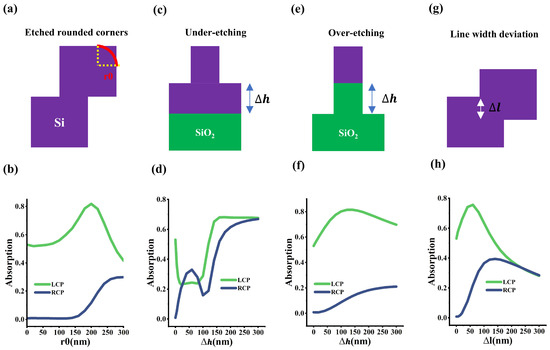
Figure 6.
The influence of the fillet radius r0, over-etching and under-etching on etching error Δh, and line width deviation Δl on CPPD. (a): The situation of etched fillet. (b): The influence of fillet radius r0. (c): The situation of under-etching. (d): The influence of under-etching error Δh. (e): The situation of over-etching. (f): The influence of over-etching error Δh. (g): The situation of line width deviation. (h): The influence of line width deviation Δl.
Tilted incident light can break the apparent symmetry of the metasurface structure, thereby inducing an equivalent chiral optical response. Therefore, monitoring the influence of the incident angle on circular dichroism seems to be an issue that cannot be ignored. The tilted incidence situation can generally be simplified into two cases: the incident light in the XZ plane and in the YZ plane. When the incident angle is α, the typical characteristic wavelength of the PMLs is λ_0/cos(α), where λ_0 is the vacuum free wavelength. For the case where the incident light is in the XZ plane, the incident azimuth angle is 0°. As shown in Figure 7a, as the incident angle increases, the circular dichroism shows a tendency to disappear. However, when α is 20 degrees, the CPQF spectrum splits, and the spectral shape splits from a single sharp peak at α = 0° into multiple wide peaks. As shown in Figure 7b, when the incident plane is the YZ plane, it can be found that although the circular dichroism gradually attenuates when the incident angle is less than 30 degrees, it still plays a role. However, when the incident angle exceeds 30 degrees, the circular dichroism basically disappears in the wavelength band from 4.0 to 4.5 μm. It can be seen that the compact circular polarization detector we designed has a relatively high collimation requirement for the incident angle, which needs to be paid extra attention in practical application scenarios.
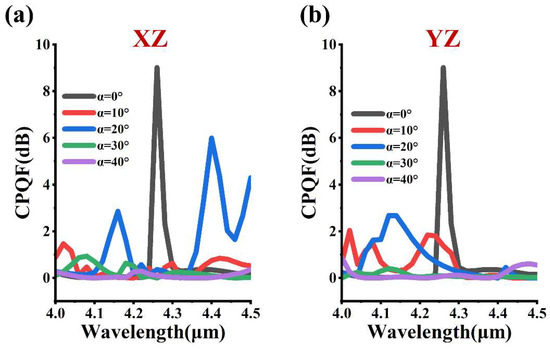
Figure 7.
The influence of the incident angle α. (a) The incident plane is the XZ plane. (b) The incident plane is the YZ plane.
4. Discussion
Circularly polarized light demonstrates superior atmospheric stability compared with unpolarized or linearly polarized light due to its unique interactions with atmospheric components. We developed a 4.26 μm circularly polarized detector via COMSOL Multiphysics simulations, utilizing a chiral silicon metasurface for polarization discrimination. This technology enables precise real-time CO2 monitoring, generating vital datasets for climate research and supporting evidence-based emission policy development.
5. Conclusions
In summary, we have designed a compact photodetector capable of directly recognizing circularly polarized light. By etching a chiral-symmetric amorphous silicon metasurface on top of the MCT detector, we achieved a CPER as high as 18 dB. This circular polarization detector has the advantages of a simple process and easy commercialization, and is likely to become a design prototype for large-scale focal plane polarization cameras. Future work should address the trade-off between optical crosstalk and array scale under small pixel pitch conditions.
Author Contributions
Conceptualization, B.C. and Y.Z.; methodology, Z.G.; software, B.C.; validation, B.C., Y.Z. and Z.G.; formal analysis, K.Z. and H.S.; investigation, K.Z. and H.S.; resources, G.S.; data curation, B.C.; writing—original draft preparation, B.C.; writing—review and editing, K.Z., G.S. and H.S.; visualization, Y.Z.; supervision, Z.G.; project administration, Z.G.; funding acquisition, G.S. All authors have read and agreed to the published version of the manuscript.
Funding
This research was funded by the Strategic Priority Research Program of the Chinese Academy of Sciences (grant no. XDB0980000).
Institutional Review Board Statement
Not applicable.
Informed Consent Statement
Not applicable.
Data Availability Statement
The raw data supporting the conclusions of this article will be made available by the authors on request.
Acknowledgments
The authors are grateful to Jietao Liu of Nankai University and Zengxuan Jiang of UCAS.
Conflicts of Interest
The authors declare no conflict of interest.
References
- Sumida, K.; Rogow, D.L.; Mason, J.A.; McDonald, T.M.; Bloch, E.D.; Herm, Z.R.; Bae, T.-H.; Long, J.R. Carbon Dioxide Capture in Metal–Organic Frameworks. Chem. Rev. 2012, 112, 724–781. [Google Scholar] [CrossRef] [PubMed]
- Bastin, J.-F.; Finegold, Y.; Garcia, C.; Mollicone, D.; Rezende, M.; Routh, D.; Zohner, C.M.; Crowther, T.W. The global tree restoration potential. Science 2019, 365, 76–79. [Google Scholar] [CrossRef] [PubMed]
- Knutson, T.R.; Tuleya, R.E.; Kurihara, Y. Simulated Increase of Hurricane Intensities in a CO2-Warmed Climate. Science 1998, 279, 1018–1021. [Google Scholar] [CrossRef] [PubMed]
- Li, D.; Zeng, N.; Zeng, M.; Liao, R.; Ma, H. Identification of Soot Particles in Air Using Polarization Scattering Method; SPIE: St Bellingham, WA, USA, 2015; Volume 9613. [Google Scholar]
- Li, Z.; Zhai, A.; Ji, Y.; Li, G.; Wang, D.; Wang, W.; Shi, L.; Ji, T.; Liu, F.; Cui, Y. Research, application and progress of optical polarization imaging technology. Infrared Laser Eng. 2023, 52, 20220808-1–20220808-16. [Google Scholar] [CrossRef]
- Wei, J.; Chen, Y.; Li, Y.; Li, W.; Xie, J.; Lee, C.; Novoselov, K.S.; Qiu, C.-W. Geometric filterless photodetectors for mid-infrared spin light. Nat. Photonics 2023, 17, 171–178. [Google Scholar] [CrossRef]
- Rubin, N.A.; D’Aversa, G.; Chevalier, P.; Shi, Z.; Chen, W.T.; Capasso, F. Matrix Fourier optics enables a compact full-Stokes polarization camera. Science 2019, 365, eaax1839. [Google Scholar] [CrossRef]
- Zhang, G.; Lyu, X.; Qin, Y.; Li, Y.; Fan, Z.; Meng, X.; Cheng, Y.; Cao, Z.; Xu, Y.; Sun, D.; et al. High discrimination ratio, broadband circularly polarized light photodetector using dielectric achiral nanostructures. Light Sci. Appl. 2024, 13, 275. [Google Scholar] [CrossRef]
- Dai, M.; Wang, C.; Qiang, B.; Jin, Y.; Ye, M.; Wang, F.; Sun, F.; Zhang, X.; Luo, Y.; Wang, Q.J. Long-wave infrared photothermoelectric detectors with ultrahigh polarization sensitivity. Nat. Commun. 2023, 14, 3421. [Google Scholar] [CrossRef]
- Fan, A.; Xu, T.; Teng, G.; Wang, X.; Xu, C.; Zhang, Y.; Li, J. Multi-angle and full-Stokes polarization multispectral images using quarter-wave plate and tunable filter. Sci. Data 2024, 11, 1401. [Google Scholar] [CrossRef]
- Goldstein, D. Polarized Light; CRC Press: Boca Raton, FL, USA, 2003. [Google Scholar] [CrossRef]
- Kliger, D.S.; Lewis, J.W.; Randall, C.E.; Azzam, R.M.A. Polarized Light in Optics and Spectroscopy. Phys. Today 1991, 44, 117. [Google Scholar] [CrossRef]
- Pendry, J.B. Negative Refraction Makes a Perfect Lens. Phys. Rev. Lett. 2000, 85, 3966–3969. [Google Scholar] [CrossRef] [PubMed]
- Pendry, J.; Schurig, D.; Smith, D. Controlling electromagnetic fields. Science 2006, 312, 1780–1782. [Google Scholar] [CrossRef]
- Guan, F.; Guo, X.; Zeng, K.; Zhang, S.; Nie, Z.; Ma, S.; Dai, Q.; Pendry, J.; Zhang, X.; Zhang, S. Overcoming losses in superlenses with synthetic waves of complex frequency. Science 2023, 381, 766–771. [Google Scholar] [CrossRef]
- Horsley, S.A.R.; Pendry, J.B. Traveling Wave Amplification in Stationary Gratings. Phys. Rev. Lett. 2024, 133, 156903. [Google Scholar] [CrossRef]
- Kuznetsov, A.I.; Brongersma, M.L.; Yao, J.; Chen, M.K.; Levy, U.; Tsai, D.P.; Zheludev, N.I.; Faraon, A.; Arbabi, A.; Yu, N. Roadmap for Optical Metasurfaces. ACS Photonics 2024, 11, 50. [Google Scholar] [CrossRef]
- Hu, J.; Zhao, X.; Lin, Y.; Zhu, A.; Zhu, X.; Guo, P.; Cao, B.; Wang, C. All-dielectric metasurface circular dichroism waveplate. Sci. Rep. 2017, 7, 41893. [Google Scholar] [CrossRef]
- Xia, Z.-S.; Liu, Y.-H.; Bao, Z.; Wang, L.-H.; Wu, B.; Wang, G.; Wang, H.; Ren, X.-G.; Huang, Z.-X. Strong circular dichroism chiral metasurfaces generated by quasi bound state in continuum domain. Acta Phys. Sin. 2024, 73, 178102. [Google Scholar] [CrossRef]
- Zhou, Y.; Huang, B.; Wang, Z.; Hong, W. Chiral metasurfaces with stabilized high circular dichroism empowered by BICs. Opt. Commun. 2024, 568, 130703. [Google Scholar] [CrossRef]
- Wu, R.-L.; Li, J.-S. Circular/linear dichroism and anisotropy based on tunable terahertz metasurfaces. J. Comput. Electron. 2024, 23, 348–357. [Google Scholar] [CrossRef]
- Liu, Z.; Xu, Y.; Ji, C.-Y.; Chen, S.; Li, X.; Zhang, X.; Yao, Y.; Li, J. Fano-Enhanced Circular Dichroism in Deformable Stereo Metasurfaces. Adv. Mater. 2020, 32, 1907077. [Google Scholar] [CrossRef]
- Li, L.; Wang, J.; Kang, L.; Liu, W.; Yu, L.; Zheng, B.; Brongersma, M.L.; Werner, D.H.; Lan, S.; Shi, Y.; et al. Monolithic Full-Stokes Near-Infrared Polarimetry with Chiral Plasmonic Metasurface Integrated Graphene–Silicon Photodetector. ACS Nano 2020, 14, 16634–16642. [Google Scholar] [CrossRef] [PubMed]
- Hu, Y.; Wang, Y.; Sang, T.; Yang, G. Mid-infrared circular-polarization-sensitive photodetector based on a chiral metasurface with a photothermoelectric effect. Appl. Opt. 2023, 62, 8. [Google Scholar] [CrossRef]
- Zuo, J.; Bai, J.; Choi, S.; Basiri, A.; Chen, X.; Wang, C.; Yao, Y. Chip-integrated metasurface full-Stokes polarimetric imaging sensor. Light Sci. Appl. 2023, 12, 218. [Google Scholar] [CrossRef]
- Deng, J.; Shi, M.; Liu, X.; Zhou, J.; Qin, X.; Wang, R.; Zhen, Y.; Dai, X.; Chen, Y.; Wei, J.; et al. An on-chip full-Stokes polarimeter based on optoelectronic polarization eigenvectors. Nat. Electron. 2024, 7, 1004–1014. [Google Scholar] [CrossRef]
- Liu, S.; Yu, F.; Liu, X.; Zhang, H.; Ma, M.; Zhang, S.; Guo, H.; Hu, H.; Yuan, C.; Zheng, Z.; et al. High-performance integrated circularly polarized light detection using soft-helix-decorated perovskite diodes. Newton 2025, 1, 100003. [Google Scholar] [CrossRef]
- Gansel, J.K.; Thiel, M.; Rill, M.S.; Decker, M.; Bade, K.; Saile, V.; von Freymann, G.; Linden, S.; Wegener, M. Gold Helix Photonic Metamaterial as Broadband Circular Polarizer. Science 2009, 325, 1513–1515. [Google Scholar] [CrossRef]
- Rumyantsev, V.V.; Mazhukina, K.A.; Utochkin, V.V.; Kudryavtsev, K.E.; Dubinov, A.A.; Aleshkin, V.Y.; Razova, A.A.; Kuritsin, D.I.; Fadeev, M.A.; Antonov, A.V. Optically pumped stimulated emission in HgCdTe-based quantum wells: Toward continuous wave lasing in very long-wavelength infrared range. In Proceedings of the 2024 Photonics & Electromagnetics Research Symposium (PIERS), Chengdu, China, 21–25 April 2024; pp. 1–7. [Google Scholar] [CrossRef]
- Dai, M.; Wang, C.; Qiang, B.; Wang, F.; Ye, M.; Han, S.; Luo, Y.; Wang, Q.J. On-chip mid-infrared photothermoelectric detectors for full-Stokes detection. Nat. Commun. 2022, 13, 4560. [Google Scholar] [CrossRef]
Disclaimer/Publisher’s Note: The statements, opinions and data contained in all publications are solely those of the individual author(s) and contributor(s) and not of MDPI and/or the editor(s). MDPI and/or the editor(s) disclaim responsibility for any injury to people or property resulting from any ideas, methods, instructions or products referred to in the content. |
© 2025 by the authors. Licensee MDPI, Basel, Switzerland. This article is an open access article distributed under the terms and conditions of the Creative Commons Attribution (CC BY) license (https://creativecommons.org/licenses/by/4.0/).