Abstract
All-optical matching systems that detect and localize designated target sequences in input all-optical data sequences have attracted significant attention in all-optical processing. They have various applications, including all-optical intrusion detection, optical frame alignment, and optical package identification. In real-world applications, noise is inevitable and can lead to incorrect matching results. In particular, noise accumulates in serial all-optical matching systems, rendering the systems useless after several cycles. In this study, we developed a scheme for suppressing noise in quadrature phase-shift-keying (QPSK)-oriented all-optical matching systems. First, we evaluated the impact of input and amplifier noise on a QPSK-oriented all-optical matching system at a transmission rate of 100 Gbaud. We then developed a second-order noise-suppression structure using a highly nonlinear fiber (HNLF). With an input optical signal-to-noise ratio (OSNR) of 6 dB and an amplifier noise figure (NF) of 4 dB, the QPSK-oriented all-optical matching system without the noise-suppression structure output incorrect results. However, when the system was optimized using the proposed noise-suppression structure, correct matching results were obtained. Furthermore, when the NF of the amplifiers was fixed at 4 dB, the optimized system could reduce the minimum input OSNR to 0 dB. With an input OSNR of 0 dB, the logarithm of the bit error rate (BER) of the output matching results of the optimized system tended to negative infinity. The extinction ratio (ER), contrast ratio (CR), and quality (Q) factor of the output of the optimized system were 154.9532, 166.94289, and 161.12 dB, respectively, indicating high noise resistance. These results demonstrate that the system optimized using the proposed noise-suppression scheme exhibits high stability and reliability in noisy environments.
1. Introduction
As cloud computing, big data, and large models continue to evolve, there has been a significant increase in the traffic carried by optical networks. In addition to the demand for high bandwidth and high-speed transmission, there is increasing concern about the security and reliability of optical networks [1,2]. Various technologies, including optical code-division multiple access (OCDMA) [3], quantum encrypted technology [4], chaos encryption technology [5], and photonic firewall technology [6,7], have been proposed to address these concerns. A photonic firewall that directly performs data identification and intrusion detection at the optical layer can be used as a high-speed and low-energy network security tool. Wirespeed Security Domains using Optical Monitoring (WISDOM), a European Union project, was the first photonic firewall developed [7]. The all-optical matching system is a core part of the photonic firewall. It comprises all-optical logic gates, such as the AND, NOT, and XOR gates, which can be obtained using dielectric waveguides [8,9], semiconductor optical amplifiers (SOAs) [10,11,12], highly nonlinear fiber (HNLF) [13], etc. Several structures of all-optical matching systems have been developed. In [13], the authors proposed an all-optical matching system for on-off keying (OOK)-modulated optical signals based on the effects of cross-phase modulation (XPM) and four-wave mixing (FWM) in HNLF. In this system, the data rate of the optical signal can reach 160 Gbps. Zhang et al. proposed an all-optical matching system for optical signals modulated by quadrature phase-shift keying (QPSK) [14]. This system simultaneously identifies the in-phase (I) and orthogonal (Q) branches, and recognition of the entire target pattern depends on whether the highest level is in the same symbol in the electrical domain and requires complicated synchronization technology. Shi et al. also proposed an all-optical matching system based on interference effects [15]. The system is suitable for any amplitude- and phase-modulation format. In the simulations, optical signals with a symbol rate of 100 GBaud and modulation formats of binary phase-shift keying (BPSK), QPSK, 8-phase-shift keying (8PSK), and 16-quadrature amplitude modulation (16QAM) were verified. Tang et al. proposed a reconfigurable all-optical pattern-matching system based on phase-sensitive amplification (PSA) using HNLF [16]. This system is suitable for the modulation formats of BPSK and QPSK. Ruan et al. developed a phase-locking-free all-optical matching system based on squarers and negators for 100-Gbaud QPSK optical signals [17]. These all-optical matching systems have contributed significantly to the implementation of photonic firewalls.
However, most all-optical matching systems are mainly verified through simulations, which create an ideal environment without noise. In actual applications, noise is inevitable and can lead to incorrect matching results. In this study, we investigated the effects of noise on the QPSK-oriented all-optical matching system reported in [16]. In addition, we studied how to reduce the influence of noise on the all-optical matching system to improve its matching results in real applications. Several theoretical and experimental studies have been conducted to improve the extinction ratio (ER) and contrast ratio (CR) of the output signal of all-optical matching systems and achieve noise compression through all-optical processing. Because the final matching results of QPSK-oriented matching systems are represented by the power of the optical signal, it is important to reduce the effect of noise on the final power. Studies on the anti-noise of the optical signal’s power have mostly employed the high nonlinearity of all-optical devices to achieve noise suppression. The most common method is the use of a reamplification and reshaping (2R) regenerator based on the self-phase modulation (SPM) effect, including optical amplifiers, high-nonlinearity devices, and filters. This technique broadens the spectrum through the SPM effect and uses a filter with a certain deviation away from the center frequency to save the optical signal and filter out noise. M. Matsumoto et al. proposed an all-optical regeneration circuit based on the SPM effect [18]. The circuit regenerates deteriorated 10 Gbps return-to-zero (RZ) code modulation signals. J. Suzuki et al. employed the XPM effect in HNLF to achieve the all-optical regeneration of 40 Gbps OOK signals [19]. Cai et al. optimized the parameters of an attenuator-based nonlinear-optical loop mirror (Att-NOLM) to perform the phase-preserving amplitude regeneration of MPSK [20]. X. Chen et al. reported 2R regeneration based on the cross-gain compression (XGC) effect in SOA at a speed of 100 Gbps with the RZ-OOK format [21]. Shao et al. used a wavelength-shift-free, single-SOA regenerator to achieve the noise suppression of the 28 Gbps signal [22] in 2020. Recent studies have focused on achieving anti-noise functions using the FWM effect. Based on the FWM effect, N.S. Mohd Shah et al. used higher-order idler light as the regenerated signal to achieve all-optical regeneration [23]. X. Zhou et al. reported multiwavelength 2R regeneration for RZ-modulated OOK signals based on the FWM effect using idler frequency light as the regenerated signal [24]. Li et al. proposed and simulated an all-optical regeneration and format conversion scheme about the input 4APSK signal based on the FWM and SPM effects in HNLF in 2023 [25]. Noise suppression based on the FWM effect is achieved by sending the signal and pump lights to highly nonlinear optical devices, generating an idler light with the same characteristics as the signal light at a new frequency and using the saturation effect to make a limiter to suppress noise. Compared with the SPM and XPM effects, the FWM effect exhibits the best shaping effect. However, when using the FWM effect of HNLF to suppress noise, the input power required for signal regeneration is limited. Noise-suppression structures, therefore, expand the range of the input power. Guo et al. proposed a second-order noise-suppression structure based on HNLF for OOK-oriented all-optical matching systems [26].
In this study, we investigate an anti-noise, phase-modulated all-optical matching system and develop a second-order noise-suppression structure to optimize the QPSK-oriented all-optical matching system. We evaluate the influence of noise, including the input and amplifier noise, on the QPSK-oriented all-optical matching system. We verify the effectiveness of the developed second-order noise-suppression structure at a transmission rate of 100 Gbaud. We also evaluate the ER, CR, quality (Q) factor, and logarithm of the bit error rate (BER) of the matching results. Compared with the system in [16], the optimized system demonstrates superior noise immunity while achieving reduced system complexity, fewer amplifier requirements, and lower power consumption.
The remainder of this paper is organized as follows. Section 2 discusses the QPSK-oriented all-optical matching system reported in [16] and analyzes the noise in the system. Section 3 proposes a second-order noise structure and discusses its principles and functions. Section 4 validates and evaluates the performance improvement of the optimized system using the second-order noise-suppression structure through simulations using VPItransmissionMaker 8.5. Section 5 describes the limitations of the proposed scheme and discusses future challenges. Section 6 concludes this paper.
2. QPSK-Oriented All-Optical Matching System and Noise Analysis
2.1. QPSK-Oriented All-Optical Matching System
Tang et al. proposed a QPSK-oriented all-optical matching system based on PSA using HNLF [16]. Figure 1 shows the structure of the matching system. First, the input QPSK data are split into two identical optical signals using a 1:2 power splitter. The first optical signal passes through the PSA module, and symbols with phases of and are amplified, whereas the power of symbols with phases of and is compressed to 0, resulting in the to be matched. The other optical signal also passes through another PSA module, which amplifies symbols with phases of and , while symbols with phases of and have their power compressed to 0, resulting in the matching of . Target signals are then generated by controlling the two BPSK signal sources, Targets 1 and 2. When the target symbol is or , Target 1 outputs the signal, and Target 2 outputs 0. When the target symbol is or , only Target 2 outputs the signal, and Target 1 outputs 0. The upper and lower parts of the symbol-matching module are identical. The upper part matches with Target 1. is split into two paths by the 1:2 power splitter. One path is input into a frequency converter to obtain a signal with frequency , and the other path is multiplexed with one of the signals obtained from Target 1 after passing through the 1:2 power splitter. After multiplexing, the result is combined with the frequency-converted signal and passes through the first AND gate. The output signal of the first AND gate is then combined with another signal obtained by splitting Target 1 and input into the second AND gate to eliminate the impact of mismatching positions. The lower part follows the same principle to match with Target 2. By multiplexing the outputs of both parts, the symbol-matching results can be obtained.
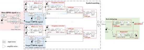
Figure 1.
QPSK-oriented all-optical matching system in [16].
Based on the order and number of symbols in the target sequence, the symbol-matching module sequentially outputs N frames of the symbol-matching signals. The signals output by the symbol-matching module are input to a recirculating loop composed of an AND gate and a regenerator. The first frame of the symbol-matching signal is subjected to an AND logic operation with the initial pulse to obtain the first frame-matching result. After regeneration and delay, the first frame-matching result is subjected to an AND logic operation with the second frame of the symbol-matching signal output by the symbol-matching module to output the second frame-matching result. This process continues in sequence, and the all-optical matching system outputs a total of N frames of matching results. The matching result of the frame represents the match between the sequence formed by the first k symbols of the target sequence and the data sequence. The number of high-power optical pulses in the matching result indicates the number of times the sequence appears in the data sequence, and the position of the high-level pulse corresponds to the last symbol of the sequence in the data sequence. The frame result indicates the overall matching result of the system for the entire target sequence.
The design of this system focuses primarily on achieving a match without optimizing its noise resistance. Input and amplifier noise introduced by the extensive use of erbium-doped fiber amplifiers (EDFAs) affect the matching performance of the system and may lead to errors in the output results. Therefore, there is a need to evaluate the impact of noise on the system matching effects and to develop appropriate noise-suppression schemes to overcome this challenge. Such schemes would allow the QPSK-oriented all-optical matching system to output stable and high-quality optical signals under the influence of noise at a rate of 100 Gbaud.
2.2. Noise in the QPSK-Oriented All-Optical Matching System
In the QPSK-oriented all-optical matching system, noise comes from two main sources: input noise and amplifier noise.
The input noise refers to the noise accumulated in the input QPSK signal before entering the system. This noise causes fluctuations in the amplitude and phase shift of the QPSK signal, thereby reducing the quality of the signal. The sources of the input noise are as follows:
(1) Optical transmitter: In practical applications, due to the limitations of devices such as lasers and modulators, the transmitted signal in the optical transmitter is not ideal. Despite the stabilization of all operating conditions, including bias, light reflections, and temperature, the laser output light intensity and phase can fluctuate, resulting in relative intensity noise (RIN), which limits the achievable signal-to-noise ratio (SNR) of the emitted signal.
(2) Optical transmission: When signals are transmitted through optical fibers, they are affected by nonlinear effects and dispersion. For communication systems using wavelength-division multiplexing technology, during optical transmission, nonlinear effects, such as FWM and XPM, and mode dispersion occur between lights of different frequencies, thereby reducing the quality of the signals. The single-mode transmitted optical signals are affected by the material, waveguide, and polarization mode dispersion in the optical fiber. In addition, during long-distance transmission, the amplifiers in the transmission link introduce noise.
In the all-optical matching system, the composition of the input noise is complex. In coherent optical communication systems, the generalized signal-to-noise ratio (GSNR) is commonly employed to unify the optical signal-to-noise ratio (OSNR) with impairments (dispersion and nonlinear effects), as expressed in Equation (1). Here, can be estimated using the Gaussian noise model [27]. In the field of optical transmission, a lot of research focuses on the GSNR [28,29]. When the input noise is dominated by amplified spontaneous emission (ASE) noise and thermal noise, it can be described using an additive Gaussian white noise (AWGN) model. In this study, we consider such input noise conditions and thus utilize the NoiseWhiteGaussOpt module in VPItransmissionMaker to simulate input noise. We use the OSNR to quantify the impact of input noise, which is expressed in Equation (2), where is the power of the input signal and is the power of the Gaussian white noise. Figure 2 shows the changes in the constellation diagram of the QPSK optical signal under different input OSNRs. By keeping the power of the input signal constant, the input OSNR can be reduced by increasing the power of the Gaussian white noise. As the input OSNR decreases, the amplitude and phase fluctuations of the QPSK optical signal increase. Therefore, we can assume that under this condition, phase noise is also included.
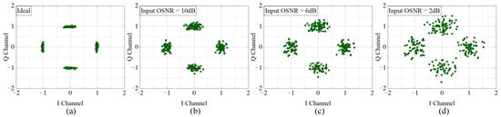
Figure 2.
QPSK optical signal constellation diagram under different input OSNR levels: (a) ideal scenarios, (b) input OSNR = 10 dB, (c) input OSNR = 6 dB, (d) input OSNR = 2 dB.
The noise from the amplifiers also affects the performance of the system. To meet the power requirements of the input signal for various modules, multiple EDFAs are employed in the QPSK-oriented all-optical matching system to amplify the optical signal, which introduces amplifier noise, including shot noise, beat noise, ASE noise, and frequency-difference noise.
Among the four types of noise generated by EDFAs, ASE noise is considered a type of shot noise because of the spontaneous emission process of the optical amplifier. In addition, because it arises from the quantum properties of photons, it is also considered a type of quantum noise. Beat noise is also a type of quantum noise because it primarily originates from the amplitude and phase fluctuations of light waves during the mixing process, which also involves the wave and quantum properties of light. Quantum noise is a special type of noise that originates from the uncertainty principles of quantum mechanics and the wave properties of photons. The frequency-difference noise is usually not classified as typical quantum noise, although its generation process also involves the quantum properties of light. This is because its characteristics are more related to optical nonlinearity, such as amplitude and phase fluctuations in nonlinear optics. Therefore, frequency-difference noise is considered a type of nonlinear noise. For the QPSK-oriented all-optical matching system, ASE noise from all EDFAs is mainly considered for the following reasons:
(1) Fundamental noise source: ASE noise is a fundamental noise source in EDFAs and is generated by the spontaneous emission of photons from erbium ions in the doped fibers as they transition from higher to lower energy states. This process is random and inherent to the amplification mechanism, making ASE noise an unavoidable component of EDFA signal amplification.
(2) Impact on SNR: ASE noise directly affects the SNR of the amplified signal. As ASE noise accumulates over multiple matching cycles, it reduces the quality of the optical signal, thereby increasing the BER and reducing the performance and capacity of the matching system. Maintaining a high SNR is essential for achieving reliable and efficient optical matching; thus, ASE noise in EDFAs must be managed efficiently.
(3) Gain saturation effects: ASE noise contributes to gain saturation in EDFAs, where an increase in the input signal power does not proportionally increase the output power due to the depletion of the available gain medium. ASE noise consumes a portion of the gain that would otherwise be dedicated to signal amplification, thereby necessitating meticulous gain management and EDFA design to achieve optimal performance. The intensity of the ASE noise is usually indicated by the power spectral density. The power spectral density of continuous broadband noise is expressed in Equation (3) [30]:
where is the power spectral density of the ASE noise in watts per hertz (W/Hz ), h is the Planck constant (approximately 6.626 × 10⁻³⁴ J·s), ν is the frequency (Hz), is the photon number density (Photons/m3), and G is the amplifier gain. This equation describes the relationship between the ASE noise and the amplifier gain, photon number density, and carrier frequency of the amplified signal. The power spectral density of ASE noise increases with frequency because ASE noise is continuous within the operating frequency range of optical communication systems. When the EDFA gain increases, the ASE noise it generates also increases. Therefore, it is necessary to reduce the use of high-gain EDFAs in the system.
It should be noted that due to design limitations in the original system [16], the interference between the PSA-processed signal and the local target sequence cannot completely eliminate power at the positions of mismatched symbols. Residual pulses with power equal to one-quarter of the “1”-level power remain, which we define as mismatch noise. Figure 3 illustrates the process of generating mismatch noise. Assume the input QPSK optical signal takes the sequence , with both the input optical signal and the local target sequence signal maintaining an identical power level P. If the target symbol is , the ideal interference matching should produce a high-power pulse exclusively at the fourth position () while suppressing all other positions to near-zero power levels. The input QPSK optical signal splits into two paths, with the upper path passing through the PSA module in the upper arm, where the power at symbols and is compressed to zero before interfering with Target 1, although residual power of P remains at positions 0 and . Similarly, the lower path undergoes processing through the PSA module in the lower arm, which compresses the power at symbols 0 and to zero prior to interference with Target 2, resulting in destructive interference that nullifies power at , while constructive interference amplifies to power , yet residual power of P persists at the mismatched positions (0 and ).
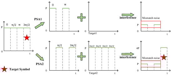
Figure 3.
Mismatch noise in the signal after interference.
To mitigate the impact of mismatch noise, [16] employed two cascaded AND gates for processing. However, this configuration requires four EDFAs. The entire system ultimately utilizes seven EDFAs, with some amplifiers exhibiting gain coefficients exceeding 20 dB, which introduces significant amplifier noise. In VPItransmissionMaker simulations, the noise figure (NF) is used to describe the noise introduced by the EDFAs. Most commercially available EDFAs have an NF below 5 dB, and AInair Labs’ Ultra-Low-Noise Optical Amplifier (LNA-220) can reduce the NF below 4 dB [31]. Therefore, for subsequent simulations, we set the NF of the EDFAs to 4 dB to model the influence of the amplifier noise on the system.
3. Second-Order Noise-Suppression Structure
After phase compression in the PSA module, the input QPSK optical signal interferes with the local target-sequence optical signal, converting the symbol information originally in phase into amplitude information. The PSA module converts the phase noise into amplitude noise. Therefore, it is necessary to design a noise-suppression structure that can reamplify and reshape the signal amplitude to enhance the system’s resistance to noise. To meet the system’s 100 Gbaud rate requirement while enabling signal reshaping after interference to counteract mismatch noise and input noise effects, we adopted the second-order noise-suppression structure based on HNLF from [26] and optimized its parameters according to the system’s nodal power level.
When two high-power optical signals of different frequencies are injected into HNLF, a new optical signal is generated at another frequency due to the FWM effect of the fiber. This new optical signal is referred to as idler light, and the two input optical signals are called the signal and pump lights. However, there are many idler frequencies generated after the FWM effect; thus, the most appropriate idler frequency must be selected. As shown in Figure 4, the pump light with frequency and the signal light with frequency generate a new idler optical signal at frequency after the FWM effect. This idler optical signal carries the information in the signal light.
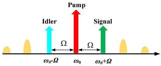
Figure 4.
Schematic of the FWM effect.
The FWM of HNLF is the core of the noise-suppression structure. Assuming that the power of the pump light is at a frequency and the power of the signal light is at a frequency , they generate a new idler optical signal at a frequency . Considering the effects of SPM and XPM, the coupled nonlinear Schrodinger equations of the pump light, signal light, and idler optical signal are expressed as shown in Equations (4)–(6) [32]:
where is the slowly varying amplitude of each signal pulse envelope, is the signal loss coefficient, is the nonlinear coefficient, and is the phase matching factor.
In the application of noise suppression based on FWM, the most important part is the change curve of the power of the idler optical signal following the signal light (the power transfer curve). The shape of the curve directly determines the noise-suppression performance of the structure. A stepped power transfer curve indicates better noise suppression.
The following equations are derived from Equations (4)–(6):
where , , and are the powers of the pump light, signal light, and idler optical signal, respectively, and , where , , and are the phases of the pump light, signal light, and idler optical signal, respectively.
When the parameters of the pump light, signal light, and HNLF are known, the numerical solution of Equations (7)–(10) [32] can be obtained using the Runge–Kutta method, and the power transfer curve can be drawn using the numerical solution.
In the QPSK-oriented all-optical matching system, the information is primarily represented by the power levels of each symbol in the signal. However, noise within the system can affect the power of the optical pulses in the output signal. Consequently, the powers of the low-power optical pulse representing “0” and the high-power optical pulse representing “1” may become similar, causing errors during the logic calculations of the optical signal. This can lead to incorrect final matching results. Using a noise-suppression structure, power amplification and shaping can be applied to the optical signal. In principle, the noise-suppression structure adjusts the input–output relationship of the signal power. Figure 5 shows a graphical representation of the noise-suppression process. When the power of the input signal lies in the AB section, the output power signal can be suppressed to 0 mW. When the power of the input signal reaches the BC section, the power of the output signal is a certain value D, which can be set manually. Finally, the noise-affected input signal is regenerated into the red signal and output, as shown in Figure 5. The longer the length of section BC, the better the noise-suppression effect.
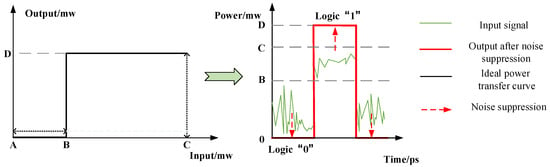
Figure 5.
Ideal power transfer curve of the second-order noise-suppression structure.
Figure 6 shows the second-order noise-suppression structure. The input signal and pump light 1 (P1) enter HNLF1 for the first FWM and then filter the signal at the desired frequency through the first filter (BPF1). The signal outputs from BPF1 and pump light 2 (P2) enter HNLF2 through the multiplexer for the second FWM, and the filter (BPF2) outputs the suppression result. The power transfer curve of the second-order noise-suppression structure is similar to the step curve.
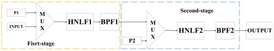
Figure 6.
Second-order noise-suppression structure.
Figure 7 shows the noise-suppression process of this structure. Figure 7a shows the power transfer curve for the first-stage noise-suppression structure. The output power ranges from A to B when the power of the input optical signal varies between C and D. The output from the first-stage noise-suppression structure is then input into the second-stage structure, and the corresponding power transfer curve is shown in Figure 7b. When the output of the first-stage noise-suppression structure is between A and B, the output of the second-stage structure maintains a relatively stable value. Figure 7c shows the power transfer curve of the input signal and output of the second-order noise-suppression structure. When the power of the input signal is between C and D, the system outputs a stable value P. Through this second-order suppression structure, the power of the high-power optical pulses in the output signal can be controlled to a relatively stable value, and the low-power optical pulses are compressed to near zero, ensuring a quality output optical signal from the system. Because , the length of the flat region is significantly increased compared to that of the single-order structure, and it is easy to limit the output power to a certain range. Therefore, the second-order noise-suppression structure can effectively suppress noise, thereby reducing the impact of noise on the all-optical matching system.
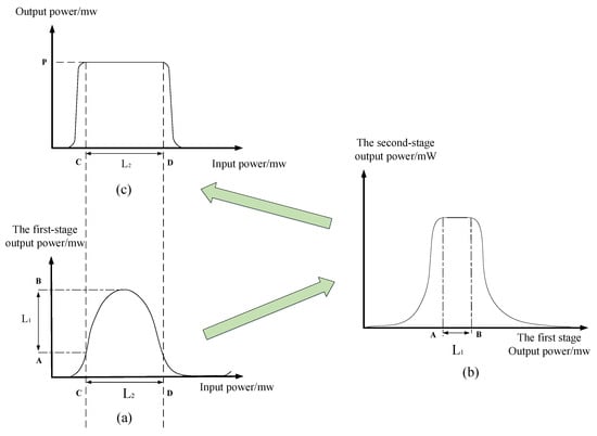
Figure 7.
Power transfer process in the second-order noise-suppression structure: (a) power transfer curve of the first-stage noise-suppression structure; (b) power transfer curve of the second-stage noise-suppression structure; (c) power transfer curve of the second-order noise-suppression structure.
The output performance of the structure can be evaluated using parameters such as the ER, CR, Q factor, and BER. The ER and CR are expressed in Equations (11) and (12) [33], where is the minimum value of the peak power of logic “1”, is the maximum value of the peak power of logic “0”, and and are the mean values of the peak powers of logics “1” and “0”, respectively. Ideally, when the input is a QPSK signal without noise, the ER and CR of the output of the multiplexer are infinite.
4. Analysis and Simulation
4.1. Noise Analysis
According to the analysis in Section 2, the main types of noise present in the all-optical QPSK-oriented matching system are input, amplifier, and mismatch noise. Tang et al. used cascaded AND gates to eliminate mismatch noise [16]. In this subsection, we analyze the effects of input and amplifier noise on the original system (hereafter, we refer to the QPSK-oriented all-optical matching system in [16] as the “original system” for brevity). First, the effects of input and amplifier noise on the original system are analyzed. Next, the matching results of the original system when both types of noise co-exist are analyzed. Figure 8 shows the simulation results of the original system in an ideal scenario and three noise scenarios. In VPItransmissionMaker 8.5, the NoiseWhiteGaussOpt module was used as input noise. The amplifier noise was characterized by an NF of 4 dB, with the noise center frequency set at 194 THz. In the simulations, the input QPSK optical signal adopted the Non-Return-to-Zero (NRZ) coding format. The data sequence for the simulations was , and the target sequence was .
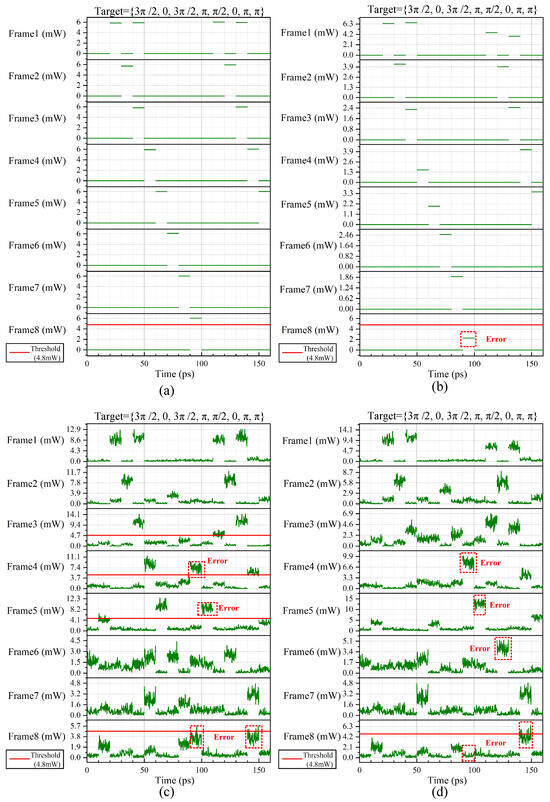
Figure 8.
Simulation results of the original system in an ideal scenario and in various noise scenarios: (a) ideal scenario, (b) input OSNR = 6 dB, (c) NF of EDFAs = 4 dB, and (d) input OSNR = 6 dB and NF of EDFAs = 4 dB.
Figure 8a shows the simulation results of the original system under an ideal scenario. Because the length of the target sequence was eight symbols, the system output eight frames of matching results. In Frame 1, the system output the position of in the data sequence; in Frame 2, it output the position of in the data sequence; in Frame 3, it output the position of in the data sequence, and so on. In Frame 8, the system output the position of the target sequence in the data sequence. The last symbol of the target sequence corresponded to the 10th symbol of the data sequence. The output signal of the all-optical matching system served as a control signal to enable the photonic firewall to perform different operations. According to the simulation results reported by Tang et al. [16] and shown in Figure 8a, for the original system, the power of “1” in the output optical signal was approximately 6 mW, while that of “0” was approximately 0 mW. We define the judgment threshold of the output signal of the all-optical matching system as . Its value was 80% of the power of “1”. For the original system, the judgment threshold = 4.8 mW. When the power of this symbol is greater than , it is considered “1”; otherwise, it is “0”. Based on this standard, we analyzed the impact of noise on the system’s performance.
Figure 8b shows the effects of input noise on the original system when the input OSNR of the system was set to 6 dB. The input noise mainly affected the power of “1” in the output signal and had little effect on the power of “0”. When the input OSNR was 6 dB, in Frame 1, the power of two “1” symbols was less than , and the powers of all “1” symbols in Frames 2 to 8 were less than . Although the waveform of the signal was approximately correct, it may cause misjudgment of the photonic firewall in practice.
Figure 8c shows the impact of amplifier noise on the original system. The NF of all EDFAs was set to 4 dB. In the system’s AND gates and wavelength converters, the EDFAs were positioned after the filters; thus, the system could not filter out the noise introduced by the amplifiers at the output. This resulted in significant noise fluctuations in the output signal of the system. During the simulation, an erroneous output signal appeared in Frame 4, which, combined with the noise, led to errors in the final matching results. In Frame 8, the mismatched positions exhibited power levels comparable to those of the correct positions, further indicating incorrect matching results.
Figure 8d shows the simulation results of the original system under the influence of both input and amplifier noise. Errors were observed in the system outputs from Frames 3 to 7. In addition, an erroneous signal was generated in Frame 8. In particular, at the correct symbol position, only a pulse with a power of approximately 1 mW was observed; however, at the erroneous symbol position, a pulse with a maximum power exceeding 4.8 mW was output.
As shown in Figure 8, the amplifier noise affects the original system more than the input noise. Because the amplifier is placed after the filter in the original system configuration, without fully leveraging the capability of the filter to reduce the amplifier noise, even in the absence of input noise, the system may output erroneous signals. In addition, because of the two cascaded AND gates introduced to eliminate the system’s mismatch noise, four EDFAs were added to the system, resulting in the generation of a large amount of noise. The noise generated by the two EDFAs in the recirculating loop also accumulated during the matching process and significantly affected the system output. Therefore, the noise-suppression scheme should focus on reducing the effects of the internal amplifier noise on the system.
4.2. Noise Suppression
Table 1 lists the parameters used in the simulation of the second-order noise-suppression structure, and Figure 9 shows the simulation diagram. The input optical signal with a center frequency of 193.1 THz is first multiplexed with the continuous light Pump 1, whose center frequency is 193.3 THz, and then input into HNLF1, where the FWM effect occurs. After passing through BPF1 with a center frequency of 192.9 THz and a bandwidth of 100 GHz, the output of HNLF1 gives the first-stage noise-suppressed signal. This signal is multiplexed with continuous light Pump 2, whose center frequency is 193.3 THz, and then input into HNLF2, where the FWM effect reoccurs. After passing through a BPF2 with a center frequency of 193.7 THz and a bandwidth of 100 GHz, the output signal of the second-order noise-suppression structure is obtained. The power transfer curve is plotted as the power relationship between the input optical signal and the output signal.

Table 1.
Simulation parameters for the second-order noise-suppression structure.
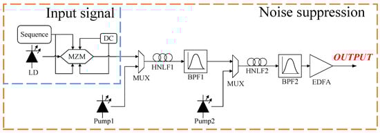
Figure 9.
Simulation diagram of the second-order noise-suppression structure.
For HNLFs, the nonlinearity coefficient is inversely proportional to the core area when all other parameters are consistent, which is expressed as . The design employs a smaller-core HNLF1 to maximize FWM efficiency through enhanced nonlinearity, while the larger-core HNLF2 strategically reduces the power density to suppress nonlinear noise and improve phase-matching tolerance. This configuration optimizes the trade-off between noise conversion efficiency and system stability. The first stage generates strong nonlinear interactions for noise suppression, while the second stage mitigates residual noise accumulation and maintains signal integrity by lowering nonlinear impairments.
Figure 10 shows the power transfer curve of the designed second-order noise-suppression structure, which was obtained through the VPItransmissionMaker simulation. When the input signal power ranges from 20 to 30 mW, the output signal power stabilizes at approximately 54 mW. However, when the input signal power falls below 15 mW, the output signal power decreases to nearly 0 mW. This noise-suppression structure effectively mitigates both input and mismatch noise, thereby enhancing the accuracy and stability of symbol matching.
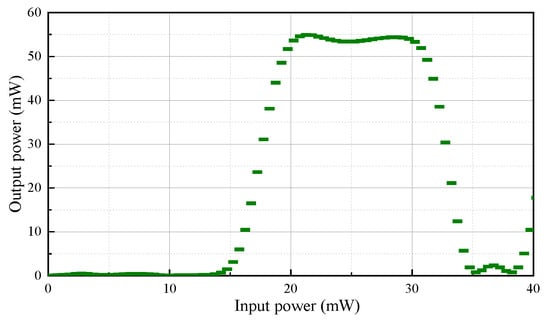
Figure 10.
Simulated power transfer curve of the second-order noise-suppression structure.
These results demonstrate that the step of the power transfer curve can be improved by cascading two single-order FWM effect noise-suppression structures. In addition, the flat area of the curve is extended, indicating that the suppression range of the symbol “1” amplitude is improved. The input signal power is appropriately amplified and maintained within the range of the flat area of the power transfer curve, thereby resulting in a more ideal noise-suppression effect.
Figure 11 shows a diagram of the QPSK-oriented all-optical matching system optimized using the proposed second-order noise-suppression structure. The second-order noise-suppression structure replaces the cascaded AND gates originally used to suppress mismatching noise, reducing the use of amplifiers while achieving better performance. In addition, an AND gate implemented based on the XPM effect [35] replaces the original AND gate in the recirculating loop. The output of the new AND gate is at the same frequency as that of its inputs; thus, a regenerator for wavelength conversion is not required. The optimized QPSK-oriented all-optical matching system uses only two EDFAs, which are five fewer than those of the original system, thereby significantly reducing the impact of amplifier noise.
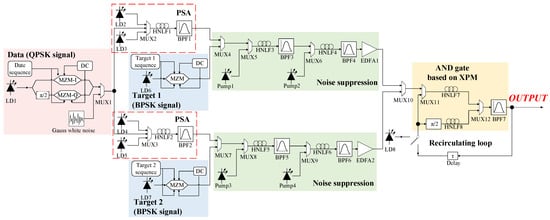
Figure 11.
All-optical matching system optimized using a noise-suppression structure.
Figure 12 shows the effect of noise suppression on the performance of the all-optical matching system. The system optimized using the proposed noise-suppression structure is hereafter referred to as the optimized system. Figure 12a shows the simulation results of the original system under an ideal scenario, and Figure 12b,c show the simulation results of the original and optimized systems, respectively, with an input OSNR of 6 dB and EDFA NF of 4 dB. Without noise suppression, the original system under a noise scenario could not output correctly matching results. In Frame 8, the power level at the 10th symbol, where a high-power optical pulse was supposed to manifest, was unexpectedly low. The erroneous 15th symbol appeared with a pulse power that surpassed even the judgment threshold of 4.8 mW. In contrast, the optimized system output correctly matching results. In the simulation, the power of “1” in the 8 frames of matching signals was stable at 6 mW, and there was no situation below the judgment threshold or too high, whereas the power of “0” was close to 0, and the entire system exhibited good stability.
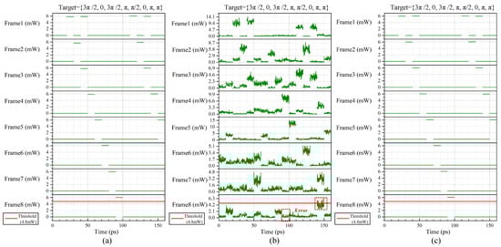
Figure 12.
Comparison of the simulation results of the all-optical matching systems: (a) original system under an ideal scenario; (b) original system with input OSNR of 6 dB and NF of EDFAs of 4 dB; (c) optimized system with input OSNR of 6 dB and NF of EDFAs of 4 dB.
To further investigate the performance of the optimized system, we maintained the NF of the EDFAs in the system at 4 dB and introduced 10 distinct noise seeds at each node, increasing the input OSNR by 2 dB per node. After averaging the simulation data obtained from each node, we plotted the ER versus input OSNR and CR versus input OSNR curves.
Figure 13 compares the relationship between the quality of the output signal and the input OSNR for the original and optimized systems. Under both input and amplifier noise, the signal quality of the optimized system was significantly improved compared with that of the original system. The ER and CR values remained above 150 and 160 dB, respectively. For the original system, with an input noise of 6 dB, the ER value decreased below 0, indicating that the system output an incorrect signal. However, for the optimized system, even when the input OSNR was 0 dB, the ER value was 154.9532 dB, and the CR value was 166.94289 dB.
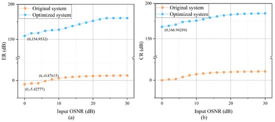
Figure 13.
Signal quality versus input OSNR curves for the optimized system: (a) ER vs. input OSNR, (b) CR vs. input OSNR.
Conversely, we also evaluated the output of the systems using the Q factor and , calculated using Equations (13) and (14), respectively. The results are listed in Table 2. The Q factor of the optimized system remained above 160 dB, and the tended toward negative infinity. These results indicate that the optimized system possesses high noise resistance and stability. The BER derived from Equation (14) served as a reference point for evaluation. Simulating the actual BER necessitates a significantly large dataset, which is beyond the scope of this study.
Table 2.
Q factor and at different input OSNRs.
5. Limitations and Challenges
5.1. Limitations in Scalability
Although the simulations yielded promising results, the current approach still has several limitations that warrant further investigation:
•Dependency on specific parameter settings: The power transfer characteristics of the noise-suppression structure vary with changes in the pump light or fiber parameters, consequently affecting output performance. This necessitates prior knowledge of the power range for both high and low signal levels during design, potentially limiting the structure’s generalizability. Under our parameter settings, input signals below 15 mW are consistently compressed to lower power levels, while those between 20 mW and 30 mW stabilize at around 54 mW.
•Sensitivity to device variations: The four-wave mixing effect demands stringent phase-matching conditions, particularly for high-power pump lights, requiring exceptional device stability. Since the noise suppression relies on four-wave mixing, optimal performance depends on highly stable laser output. Therefore, when designing the system, it is necessary to pay attention to the design of the temperature control circuit to ensure the stable operation of the lasers. In addition, the method for generating phase-locked pump light in [14] can also be used to improve the stability of the pump light in the noise-suppression structure.
•Scalability for higher-order modulation: The QPSK system requires two second-order noise-suppression structures. For all-optical matching systems handling higher-order modulation formats, additional noise-suppression structures would be needed, increasing both system complexity and power consumption. To adapt this solution for higher-order systems, careful monitoring of nodal signals throughout the all-optical matching system becomes essential to identify the optimal insertion points for noise-suppression structures, thereby minimizing overall complexity and energy consumption.
5.2. Future Challenges
Although we successfully optimized the system’s noise resistance, numerous practical challenges remain that demand careful attention and resolution:
•High-performance requirements for components: The stringent performance requirements for both the transmitter and receiver components are particularly noteworthy. To ensure signal integrity, modulators and photodetectors must meet the substantial bandwidth demands of 100 Gbaud operation. In our simulations, we investigated commercially available devices that can meet our parameter settings, such as the thin-film lithium niobate (TFLN) modulators reported in [36] and a 100 GHz balanced photodetector from Coherent [37]. However, beyond bandwidth considerations, additional critical specifications, including modulation rate and phase accuracy, impose rigorous constraints on component selection. These demanding requirements inevitably lead to significantly elevated experimental costs.
•High-precision requirements for measurement equipment: In experiments, it is necessary to monitor signals at various nodes to optimize the parameters of system components. Since key elements such as the PSA module, frequency converter, AND gate, and noise-suppression structure are all implemented based on the four-wave mixing (FWM) effect, a high-precision optical spectrum analyzer (OSA) is essential for observing nonlinear effects. This imposes stringent requirements on the OSA’s resolution and dynamic range. For example, the Yokogawa AQ6370E Telecom OSA [38] can be employed, offering a wavelength accuracy of 0.1 nm and a typical dynamic range of 78 dB. For the receiver, the oscilloscope must have a bandwidth of at least 70% of the symbol rate of the signal to fully capture signal details. Our investigation confirms that the Keysight UXR1104B Infiniium Oscilloscope [39], with a bandwidth of 110 GHz, could meet this requirement.
•Design of Temporal and Phase Synchronization: In practical implementations, precise temporal and phase synchronization of signals must be ensured. The PSA module imposes stringent phase-matching requirements between the input signal and the pump light. Additionally, the output signal from the PSA module and the local target sequence optical signal must maintain both temporal and phase synchronization to yield correct interference results. To address this, Zhang et al. proposed a phase-locked pumping method based on degenerate four-wave mixing (DFWM), ensuring phase synchronization for all PSA inputs [14]. To achieve phase synchronization between the input QPSK optical signal and the local target sequence optical signal, an optical phase-locked loop (OPLL), such as the Costas-loop-based OPLL proposed in [40] and the OPLL system implemented using an unbalanced delay interferometer in [41], is required. For the recirculating loop, achieving precise switching and delay control presents a critical challenge. Given that 100 Gbaud signals have a symbol duration of only 10 ps, picosecond-level timing accuracy in switching and delay alignment becomes a nontrivial engineering problem.
6. Conclusions
In this study, we investigated the impact of noise on the performance of QPSK-oriented all-optical matching systems and developed an effective noise-suppression scheme for the systems. We first analyzed the effects of input and amplifier noise from EDFAs on the output signal of the system. With an input OSNR of 6 dB and an EDFA NF of 4 dB, the original system output incorrect matching results due to the effects of noise. The system optimized using the proposed second-order noise-suppression structures has a simpler architecture and exhibits better noise resistance than the original system. The optimized system reduces the requirement for the minimum input OSNR to 0 dB. At an input OSNR of 0 dB, the of the optimized all-optical matching system was close to negative infinity, the ER of the output signal was 154.9532 dB, the CR was 166.94289 dB, and the Q factor was 161.12 dB, indicating that under this noise level, the optimized system can output matching results with high stability.
The proposed scheme has two second-order noise-suppression structures. In future studies, we will explore noise-suppression schemes with simpler structures and lower costs. In addition, we will study noise-suppression schemes for higher-order modulations.
Author Contributions
Conceptualization, X.L.; methodology, F.R. and T.G.; software, F.R., T.G. and Y.T.; validation, F.R. and T.G.; formal analysis, X.L. and F.R.; investigation, X.L.; resources, X.L., Y.T. and S.H.; data curation, Y.T. and T.G.; writing—original draft preparation, X.L. and F.R.; writing—review and editing, X.L. and F.R.; visualization, T.G.; supervision, X.L.; project administration, X.L.; funding acquisition, X.L., Y.T. and S.H. All authors have read and agreed to the published version of the manuscript.
Funding
This research was funded by the National Natural Science Foundation of China (62171050, 62125103), the Fundamental Research Funds for Central Universities (2024ZCJH02), the Open Fund of the State Key Laboratory of Information Photonics and Optical Communications (Beijing University of Posts and Telecommunications) (IPOC2024B06), and the Natural Science Basic Research Program of Shaanxi Province (No. 2024JC-YBQN-0685).
Institutional Review Board Statement
Not applicable.
Informed Consent Statement
Not applicable.
Data Availability Statement
The data presented in this study are available on request from the corresponding author. The data are not publicly available due to the fact that the data also form part of an ongoing study.
Conflicts of Interest
The authors declare no conflicts of interest.
References
- Dahan, D.; Mahlab, U. Security threats and protection procedures for optical networks. IET Optoelectron. 2017, 11, 186–200. [Google Scholar] [CrossRef]
- Zhao, C.; Li, X.; Xin, J.; Liu, Y.; Li, D.; Huang, S. Intelligent Agent-Based Dynamic Reliability Evaluation for Optical Networks: A Comprehensive Framework and Case Study. IEEE Commun. Mag. 2024, 63, 151–157. [Google Scholar] [CrossRef]
- Du, Y.; Xue, F.; Yoo, S.J.B.; Ding, Z. Security enhancement of SPECTS O-CDMA through concealment against upstream DPSK eavesdropping. J. Light. Technol. 2007, 25, 2799–2806. [Google Scholar] [CrossRef]
- Yin, X.; Pan, D.; Yu, H.; Huo, Y.; Li, F.; Wang, Q. Research of Long-Distance Encrypted Signal Transmission Enhancement Method Based on Quantum Communication Power System. In Proceedings of the 2018 IEEE 9th International Conference on Software Engineering and Service Science (ICSESS), Beijing, China, 23–25 November 2018; pp. 403–405. [Google Scholar] [CrossRef]
- Zhang, W.; Zhang, C.; Jin, W.; Chen, C.; Jiang, N.; Qiu, K. Chaos Coding-Based QAM IQ-Encryption for Improved Security in OFDMA-PON. IEEE Photonics Technol. Lett. 2014, 26, 1964–1967. [Google Scholar] [CrossRef]
- Yang, X.; Webb, R.; Manning, R.; Maxwell, G.; Poustie, A.; Lardenois, S.; Cotter, D. Demonstration of all-optical pattern recognition at 42Gbit/s. In Proceedings of the 2008 34th European Conference on Optical Communication, Brussels, Belgium, 21–25 September 2008; pp. 1–4. [Google Scholar] [CrossRef]
- Webb, R.P.; Yang, X.; Manning, R.J.; Maxwell, G.D.; Poustie, A.J.; Lardenois, S.; Cotter, D. All-Optical Binary Pattern Recognition at 42 Gb/s. J. Light. Technol. 2009, 27, 2240–2245. [Google Scholar] [CrossRef]
- Zhao, Y.; Lombardo, D.; Mathews, J.; Agha, I. Low-power optical logic gate in a silicon waveguide. In Proceedings of the 2017 Conference on Lasers and Electro-Optics (CLEO), San Jose, CA, USA, 14–19 May 2017; pp. 1–2. [Google Scholar]
- Butt, M.; Khonina, S.; Kazanskiy, N. Recent advances in photonic crystal optical devices: A review. Opt. Laser Technol. 2021, 142, 107265. [Google Scholar] [CrossRef]
- Lovkesh; Marwaha, A. Implementation of optical logic gates at 160 Gbps using nonlinear effect of single SOA. Opt. Laser Technol. 2015, 70, 112–118. [Google Scholar] [CrossRef]
- Siarkos, T.; Zoiros, K.E.; Nastou, D. On the feasibility of full pattern-operated all-optical XOR gate with single semiconductor optical amplifier-based ultrafast nonlinear interferometer. Opt. Commun. 2009, 282, 2729–2740. [Google Scholar] [CrossRef]
- Kotb, A.; Zoiros, K.E.; Li, W. Execution of all-optical Boolean OR logic using carrier reservoir semiconductor optical amplifier-assisted delayed interferometer. Opt. Laser Technol. 2021, 142, 107230. [Google Scholar] [CrossRef]
- Liu, Y.; Li, X.; Tang, Y.; Shi, Z.; Huang, S. Binary sequence matching system based on cross-phase modulation and four-wave mixing in highly nonlinear fibers. Opt. Eng. 2020, 59, 105103. [Google Scholar] [CrossRef]
- Zhang, Q.; Gong, X.; Guo, L. All-Optical QPSK Pattern Recognition in High-Speed Optoelectronic Firewalls. IEEE Photonics J. 2023, 15, 1–16. [Google Scholar] [CrossRef]
- Shi, Z.; Li, X.; Shi, H.; Liu, Y.; Guo, K.; Huang, S. All-optical matching structure for multi-order modulation formats. Opt. Eng. 2023, 62, 068106. [Google Scholar] [CrossRef]
- Tang, Y.; Li, X.; Shi, H.; Chang, J.; Tian, Y.; Huang, S. Reconfigurable all-optical pattern-matching system for phase modulation formats based on phase-sensitive amplification in highly nonlinear fiber. Opt. Fiber Technol. 2023, 81, 103548. [Google Scholar] [CrossRef]
- Ruan, F.; Li, X.; Shi, H.; Liu, Y.; Gao, T.; Guo, K.; Huang, S. Phase-locking-free all-optical matching system for 100 Gbaud QPSK optical signal. Opt. Express 2024, 32, 26006–26025. [Google Scholar] [CrossRef]
- Matsumoto, M.; Shimada, Y.; Sakaguchi, H. Two-Stage SPM-Based All-Optical 2R Regeneration by Bidirectional Use of a Highly Nonlinear Fiber. IEEE J. Quantum Electron. 2009, 45, 51–58. [Google Scholar] [CrossRef]
- Suzuki, J.; Tanemura, T.; Kikuchi, K. All-optical regeneration of 40-Gb/s low-Q signal using XPM-induced wavelength shift in highly-nonlinear fiber. In Proceedings of the 2005 31st European Conference on Optical Communication, ECOC 2005, Glasgow, UK, 25–29 September 2005; Volume 2, pp. 199–200. [Google Scholar] [CrossRef]
- Cai, Y.; Wen, F.; Guo, B.; Wu, B.; Qiu, K. All-optical M-PSK Signal Regeneration using a Nonlinear-optical Loop Mirror (NOLM). In Proceedings of the 2020 Asia Communications and Photonics Conference (ACP) and International Conference on Information Photonics and Optical Communications (IPOC), Beijing, China, 24–27 October 2020; pp. 1–3. [Google Scholar]
- Chen, X.; Huo, L.; Jiang, X.; Lou, C. 100-Gb/s 2R regeneration using cross gain compression in semiconductor optical amplifiers. Opt. Express 2015, 23, 23143–23154. [Google Scholar] [CrossRef]
- Shao, L.; Wen, F.; Guo, B.; Krzczanowicz, L.; Yang, F.; Wu, B.; Qiu, K. All-optical Amplitude Noise Suppression in a Nonlinear Semiconductor Optical Amplifier (SOA). In Proceedings of the 2020 Asia Communications and Photonics Conference (ACP) and International Conference on Information Photonics and Optical Communications (IPOC), Beijing, China, 24–27 October 2020; pp. 1–3. [Google Scholar]
- Mohd Shah, N.S.; Matsumoto, M. All-optical regeneration of time-interleaved multi-wavelength signals based on higher-order four-wave mixing. In Proceedings of the 2009 IEEE/LEOS Summer Topical Meeting, Newport Beach, CA, USA, 20–22 July 2009; pp. 103–104. [Google Scholar] [CrossRef]
- Zhou, X.y.; Wu, B.j.; Wen, F.; Zhang, H.c.; Zhou, H.; Qiu, K. Total date rate of multi-wavelength 2R regenerators for time-interleaved RZ-OOK signals. Opt. Express 2014, 22, 22937–22951. [Google Scholar] [CrossRef]
- Li, Q.; Wen, H.; Yang, J.; Xu, Q.; Yang, X.; Li, Y. All-Optical Regeneration and Format Conversion for 4APSK Signals Based on Nonlinear Effects in HNLF. IEEE Photonics J. 2023, 15, 1–9. [Google Scholar] [CrossRef]
- Guo, K.; Li, X.; Shi, H.; Liu, Y.; Shi, Z.; Huang, S. Noise Suppression of All-optical OOK Matching System Based on Cascaded Highly Nonlinear Fiber. In Proceedings of the 2023 21st International Conference on Optical Communications and Networks (ICOCN), Qufu, China, 31 July 2023–3 August 2023; pp. 1–3. [Google Scholar] [CrossRef]
- Poggiolini, P. The GN Model of Non-Linear Propagation in Uncompensated Coherent Optical Systems. J. Light. Technol. 2012, 30, 3857–3879. [Google Scholar] [CrossRef]
- Cho, H.J. Generalized optical signal-to-noise ratio monitoring using a convolutional neural network for digital coherent receivers. Opt. Lett. 2023, 48, 1798–1801. [Google Scholar] [CrossRef]
- Khan, I.; Bilal, M.; Umar Masood, M.; D’Amico, A.; Curri, V. Lightpath QoT computation in optical networks assisted by transfer learning. J. Opt. Commun. Netw. 2021, 13, B72–B82. [Google Scholar] [CrossRef]
- Agrawal, G.P. Loss Management. In Fiber-Optic Communication Systems; John Wiley and Sons, Ltd.: Hoboken, NJ, USA, 2011; pp. 295–344. [Google Scholar] [CrossRef]
- Alnair Labs. LNA-220 Ultra-Low Noise Amplifier. Available online: http://www.alnair-labs.com/product-lineup/product-lna-220/ (accessed on 20 December 2024).
- Hansryd, J.; Andrekson, P.; Westlund, M.; Li, J.; Hedekvist, P.O. Fiber-based optical parametric amplifiers and their applications. IEEE J. Sel. Top. Quantum Electron. 2002, 8, 506–520. [Google Scholar] [CrossRef]
- Kakarla, R.; Venkitesh, D. Demonstration of optical header recognition for BPSK data using novel design of logic gates. Opt. Commun. 2016, 363, 117–122. [Google Scholar] [CrossRef]
- Norimatsu, S.; Maruoka, M. Accurate Q-factor estimation of optically amplified systems in the presence of waveform distortions. J. Light. Technol. 2002, 20, 19–27. [Google Scholar] [CrossRef]
- Lovkesh, S.; Sharma, V.; Singh, S. The design of a reconfigurable all-optical logic device based on cross-phase modulation in a highly nonlinear fiber. J. Comput. Electron. 2021, 20, 1–12. [Google Scholar] [CrossRef]
- Xu, M.; Zhu, Y.; Pittalà, F.; Tang, J.; He, M.; Ng, W.C.; Wang, J.; Ruan, Z.; Tang, X.; Kuschnerov, M.; et al. Dual-polarization thin-film lithium niobate in-phase quadrature modulators for terabit-per-second transmission. Optica 2022, 9, 61–62. [Google Scholar] [CrossRef]
- COHERENT. 100 GHz Balanced Photodetector BPDV412xRv. Available online: https://www.coherent.com/content/dam/coherent/site/en/resources/datasheet/networking/100ghz-balanced-photodetector-ds.pdf (accessed on 20 December 2024).
- Yokogawa. AQ6370 Series Optical Spectrum Analyzer. Available online: https://cdn.tmi.yokogawa.com/1/2706/files/BUAQ6370SR-20EN.pdf (accessed on 1 May 2025).
- Keysight. Infiniium UXR-B Series Oscilloscopes. Available online: https://www.keysight.com.cn/cn/zh/assets/3123-1371/technical-overviews/Infiniium-UXR-Series-Oscilloscopes1.pdf (accessed on 1 May 2025).
- Chul Park, H.; Lu, M.; Bloch, E.; Reed, T.; Griffith, Z.; Johansson, L.; Coldren, L.; Rodwell, M. 40Gbit/s coherent optical receiver using a Costas loop. Opt. Express 2012, 20, B197–B203. [Google Scholar] [CrossRef]
- Zhang, L.; Xie, W.; Feng, Y.; Meng, Y.; Bai, Y.; Yang, J.; Wei, W.; Dong, Y. Modeling and optimization of an unbalanced delay interferometer based OPLL system. Opt. Express 2022, 30, 1994–2005. [Google Scholar] [CrossRef]
Disclaimer/Publisher’s Note: The statements, opinions and data contained in all publications are solely those of the individual author(s) and contributor(s) and not of MDPI and/or the editor(s). MDPI and/or the editor(s) disclaim responsibility for any injury to people or property resulting from any ideas, methods, instructions or products referred to in the content. |
© 2025 by the authors. Licensee MDPI, Basel, Switzerland. This article is an open access article distributed under the terms and conditions of the Creative Commons Attribution (CC BY) license (https://creativecommons.org/licenses/by/4.0/).