1. Introduction
As artificial intelligence (AI) advances, traditional electronic computing faces limitations, such as high power consumption and slow processing speeds with large-scale data. Optical computing, with its parallel processing and low energy consumption, offers a potential solution. Recently, diffractive neural networks (DNNs) have integrated optical diffraction with AI, opening new possibilities for optical computing [
1,
2]. DNNs perform computations by precisely controlling the phase and amplitude of light through multiple modulation layers, showing promise in tasks like image classification and feature detection, making them a key research focus in optical computing and AI [
3,
4,
5].
Research on DNNs has advanced significantly in recent years. Early experiments relied on 3D printing to create phase modulation layers or used devices like digital micromirror devices (DMD) and spatial light modulators (SLM) to build multilayer DNNs, demonstrating their feasibility [
1,
6,
7]. However, these approaches were limited by bulky structures, impeding miniaturized integration. Given the importance of visible light in optical computing and the push for integrated applications, research has shifted to micro-nano fabrication for compact, efficient DNN devices [
8,
9,
10,
11]. Traditional methods like lithography and plasma etching [
12,
13] can achieve high-precision layers but are hindered by long processing times and high costs, limiting rapid prototyping. In contrast, two-photon polymerization (TPP), a high-precision 3D additive manufacturing technique, has gained traction in DNN fabrication due to its rapid prototyping and design flexibility. TPP uses ultrafast laser beams to induce two-photon absorption in photosensitive materials, enabling layer-by-layer construction of complex micro-nano structures with submicron precision [
14,
15]. Widely used in bioengineering, advanced photonics, and micro-nano manufacturing, TPP is increasingly applied in optical computing and AI [
16,
17,
18,
19,
20,
21,
22,
23,
24,
25].
Despite TPP’s advantages in DNN fabrication [
26,
27], challenges remain in scaling up structures and integrating with electronic devices. The computational accuracy of DNNs depends on precise control of neuron structure heights within the phase modulation layer to achieve high-fidelity phase modulation of the optical field [
28]. This demands exceptional fabrication precision, structural consistency, and surface flatness [
29]. However, commercial TPP equipment typically has a high-precision printing range of about 200 μm, requiring stitching for larger areas. During this process, factors like substrate unevenness, thermal expansion stress, and equipment alignment errors can introduce deviations, affecting DNN performance. Substrate tilt, a key error source in TPP, leads to cumulative height deviations during large-area stitching, causing neuron structure heights to drift from design values and reducing phase modulation accuracy. Additionally, long-distance stitching amplifies the influence of the angular tilt, making it challenging to balance large travel distances with high precision. Experimental results show that DNN performance often falls short of simulation predictions [
3,
11], with phase errors from stitching and substrate tilt being the primary causes. This highlights the limitations of current fabrication techniques in rapid prototyping, that are unable to fully meet the high-precision needs of DNNs from simulation to experiment.
To address cumulative deviations from substrate tilt and stitching errors, researchers have explored various compensation strategies. Traditional micro-nano fabrication techniques [
30] often use high-precision displacement stages or real-time feedback systems (e.g., interferometers or acoustic emission sensors) to correct focus errors caused by substrate tilt, or adjust galvanometer scanning planes to align with the substrate surface [
31,
32,
33,
34,
35,
36,
37]. While these methods can reduce errors, their complexity, high cost, and sensitivity to environmental conditions limit their widespread use in standard laboratory and industrial settings.
In response, we propose an index-matching TPP (IM-TPP) process to address fabrication errors in traditional TPP caused by substrate tilt and related factors, improving the precision and reliability of DNN fabrication. IM-TPP optimizes the phase modulation layer by employing two photoresists for index matching, in contrast to traditional TPP’s single photoresist–air interface or power-adjusted refractive index approaches. This reduces the refractive index difference (RID) between structures to the order of 10
−2, effectively mitigating optical path fluctuations from substrate tilt, enhancing phase control robustness, and improving fabrication accuracy and structural uniformity. We note that recent work [
38] utilized RID optimization to fabricate chiral diffractive optical elements (DOEs), indirectly validating the reliability and potential of the IM-TPP process, and addressing the limitations of single-material processes in complex high-order structures. Similarly, our research applies refractive index-matched TPP (IM-TPP) to fabricate DNNs’ phase modulation layers, optimizing the RID between IP-Dip and IP-S photoresists to improve the accuracy and performance of DNNs devices. This demonstrates the potential of IM-TPP in both micro-nano fabrication and optical computing.
To validate the effectiveness of the IM-TPP process, we evaluated its performance in the FashionMNIST three-class classification task through simulations and experiments. The results show that DNNs fabricated with traditional TPP achieved a classification accuracy of 91.67%, while IM-TPP improved the accuracy to a range of 94.67% to 95.13%, with the highest value closely matching the simulation-predicted accuracy of 95.03%. Additionally, we performed separate simulations on other task types, which also yielded similar performance improvements. These findings demonstrate that IM-TPP not only effectively reduces fabrication errors but also provides higher reliability and precision in practical applications, offering a viable solution for the high-precision, rapid replication of DNNs from simulation to experiment.
2. Simulation and Fabrication
We trained a single-layer DNNs based on angular spectrum diffraction theory, which models light propagation between planes using fast Fourier transform (FFT), reducing the computational complexity of direct integration methods. To meet the pixel size requirements for fabrication, we used a 632.8 nm He-Ne laser and set the pixel size of the phase plate and lens phase to 4 μm × 4 μm. This design balances theoretical accuracy with practical manufacturability. Scalar diffraction theory assumes no photon polarization coupling, simplifying calculations and enabling rapid training of the phase modulation layer.
The phase value optimization was performed using the Backpropagation (BP) algorithm, combined with the SoftMax Cross Entropy (SCE) loss function and Mean Squared Error (MSE) loss function for multi-objective training. This method reduces model classification error while optimizing phase distribution smoothness and improving manufacturability. To demonstrate the application of stitching printing in phase modulation layer fabrication, we designed a 400 μm × 400 μm phase modulation layer composed of 100 × 100 pixels. Due to the limitations of commercial high NA microscopes (e.g., NA 1.4, 63 × oil immersion object), the modulation layer needed to be divided into 3 × 3 sub-regions, each measuring 140 μm × 140 μm. These regions were then stitched together during fabrication.
The model use the FashionMNIST dataset for a three-class classification task, focusing on labels 0 (t-shirt), 1 (pants), and 9 (boots). This task is representative and helps verify the classification performance of a single-layer phase-modulated diffractive neural network. The training dataset contains 10,000 images, and the test dataset contains 3000 images. In the training of DNNs, the final trained classification accuracy of the phase modulation layer reached 95.43%, with a test accuracy of 95.03%, demonstrating the potential of single-layer diffractive neural networks in simple classification tasks.
To investigate the impact of substrate tilt-induced phase errors on classification performance, we conducted numerical simulations by introducing phase delays to the original modulation layer and evaluating test set recognition. As shown in
Figure 1, assuming substrate tilt angles of 0.2° and 0.15° along the X direction, the height differences between the far-left and far-right sides of the 140 μm × 140 μm sub-region were 0.489 μm and 0.367 μm, respectively. In the traditional single-photoresist process, the RID between the phase modulation layer and air is 0.547, and the height difference corresponding to a 2π phase shift is 1.16 μm. The resulting phase delay differences are 0.843π and 0.632π. In the IM-TPP process, the RID between structures is 0.041, and the height difference corresponding to a 2π phase shift is 15.43 μm. The phase delay differences are only 0.063π and 0.048π. Since tilting could occur simultaneously in both X and Y directions, we designed additional numerical simulations to consider this more common scenario.
As shown in
Figure 2, we applied phase delays along the diagonal direction to the trained diffraction phase modulation layer and performed numerical simulations for the classification recognition of 3000 test images from FashionMNIST labels 0, 1, and 9.
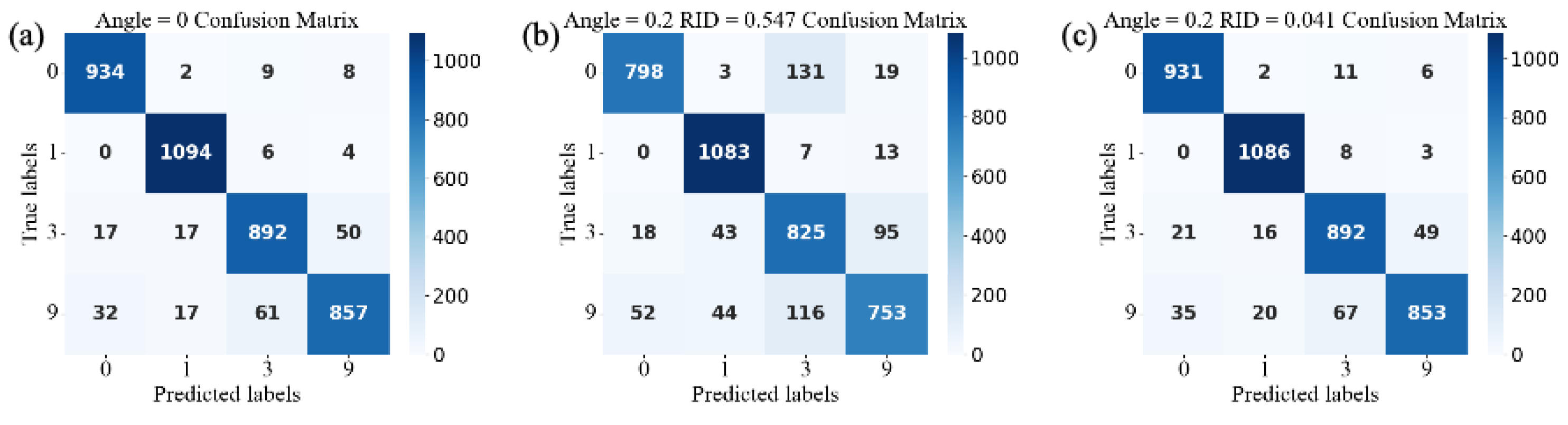
Figure 2a shows the trained DNNs’ phase modulation layer without phase errors, with classification accuracy of 95.03%, as shown in the confusion matrix. In
Figure 2b, phase tilt of 0.15° along both X and Y directions was introduced. When the modulation layer structure height was 1.16 μm, the classification accuracy from numerical simulation was 93.80%. In
Figure 2c, with the same tilt and a modulation layer structure height of 15.43 μm, the classification accuracy improved to 94.97%. In
Figure 2d, with 0.2° tilt in both directions, the modulation layer structure height remained at 1.16 μm, resulting in a classification accuracy of 91.50%. Finally, in
Figure 2e, with the same tilt and modulation layer height of 15.43 μm, the accuracy increased by 3.50% to 95.00%, nearly matching the accuracy of 95.03% without phase error. Simulation results show that by using IM-TPP to reduce phase errors introduced by tilt, the classification accuracy significantly improved, demonstrating that it can effectively reduce performance fluctuations due to processing errors in classification tasks.
To further validate its general applicability, we conducted simulations on the MNIST four-class classification task (0, 1, 3, 9). The results in
Figure 3 show that, without phase errors, the training accuracy was 94.43%. After introducing a 0.2° bidirectional tilt, the accuracy with traditional TPP dropped to 86.48%, while IM-TPP improved the accuracy to 94.05%, which is close to the error-free level. This further highlights the superiority of IM-TPP in mitigating fabrication errors and achieving high-precision replication.
The specific steps for the experimental fabrication are as follows: First, the phase modulation layer was fabricated using TPP technology with IP-Dip photoresist (refractive index 1.547, Nanoscribe). A 63× objective lens (NA = 1.4) was used, with a maximum laser average power of 50 mW. Under this setup, we selected 40% power (i.e., 20 mW), a scanning speed of 10 mm/s, a hatching distance of 0.1 μm, and a slicing distance of 0.3 μm. This parameter configuration ensured the fine detail and smoothness of the structure. After exposure, chemical development was used to remove the uncured photoresist: the sample was immersed in propylene glycol monomethyl ether acetate (PGMEA) for 20 min, followed by a 4-min rinse in isopropanol, and finally a 1-min soak in electronic fluoridation liquid to thoroughly remove any residue.
After development, IP-S photoresist (refractive index 1.506, Nanoscribe) was applied to cover the phase modulation layer. For the covering layer, a 25× objective lens was used, with the laser power set to 60% (i.e., 30 mW based on a maximum average power of 50 mW), a scanning speed of 100 mm/s, a hatching distance of 0.3 μm, and a slicing distance of 0.7 μm. The 25× objective lens offers a wider field of view and higher processing speed compared to the 63× lens, making it ideal for quickly fabricating large-area covering layers while still ensuring structural quality. The same development steps (PGMEA immersion for 20 min, isopropanol rinse for 4 min, and electronic fluoridation liquid immersion for 1 min) were repeated to remove excess photoresist and ensure a clean surface.
To further optimize the process, we explored an alternative approach, using 100 μm diameter spacers to support a specific height, covering the phase modulation layer with a quartz flat mold, and curing it as a whole using ultraviolet light in the 390–480 nm range (energy density 3000 mJ/cm2). This improvement not only simplified the workflow but also enhanced the consistency and flatness of the covering layer.
3. Results
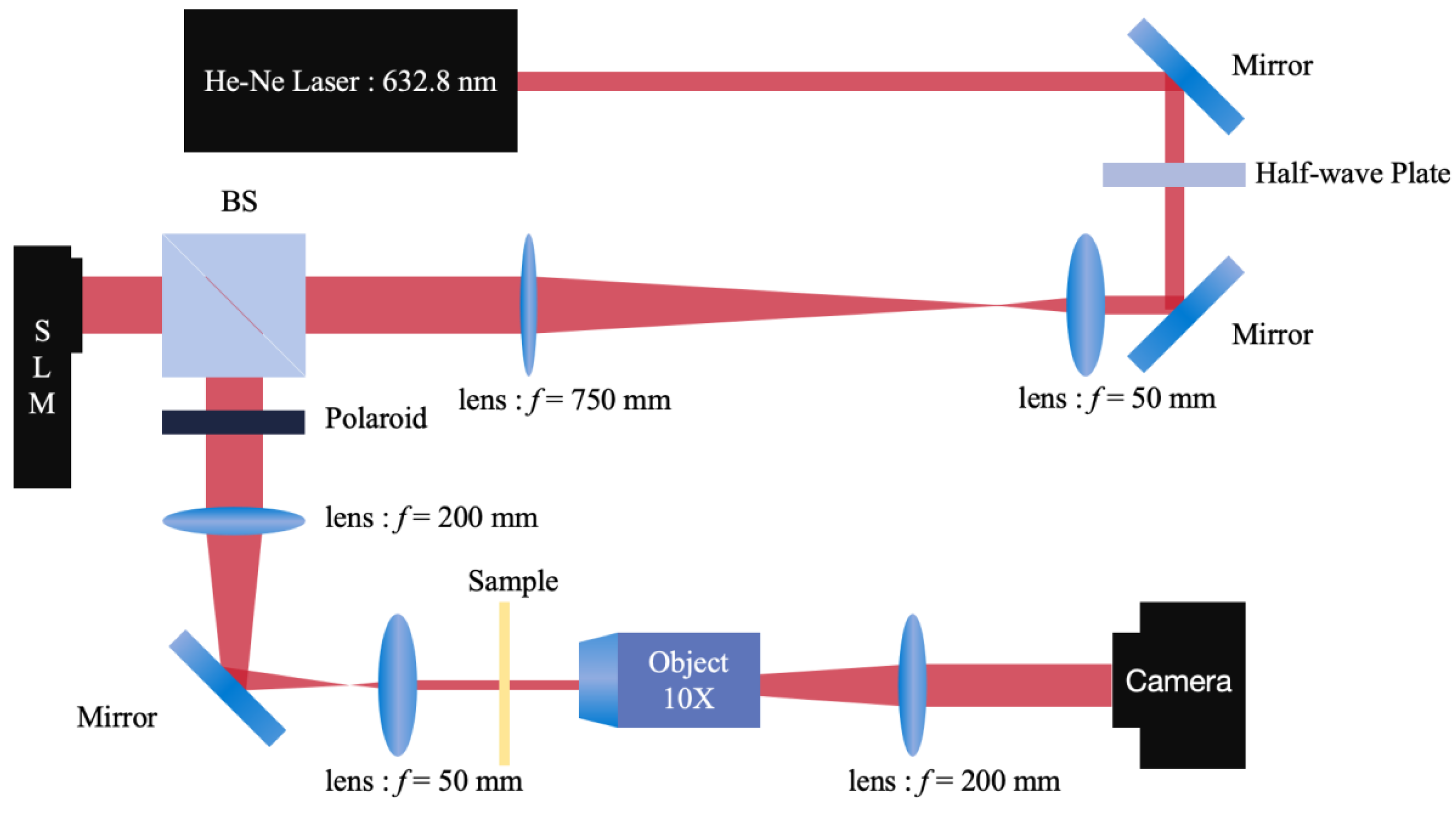
To verify the effectiveness of the proposed fabrication process in enhancing image classification accuracy, we established an optical neural network characterization platform and conducted experimental validation. As
Figure 4 show that, in the experiment, we used a 632.8 nm He-Ne laser as the light source. The beam was shaped using a 1/2 wave plate and a 4 f system, expanded, filtered through a pinhole, and then encoded onto an SLM. After beam reduction, the light was directed into the chip for the experiment.
We fabricated deep neural networks (DNNs) using the TPP process with IP-Dip photoresist (thickness 1.16 μm) and the IM-TPP process (thickness 15.43 μm). The experimental setup involved an incident light field size of 400 μm × 400 μm, with both incident and outgoing distances set to 6 mm. Classification testing was conducted using 3000 images for both samples. The DNNs fabricated with the single-photoresist TPP process achieved a classification accuracy of 91.67%, as shown in the confusion matrix in
Figure 5c, while those fabricated with the IM-TPP process reached 94.67%, as presented in
Figure 5d, closely matching the simulated accuracy of 95.03%.
The IM-TPP process reduces the refractive index difference (RID) between structures through index matching, enabling the height required for a single pixel to modulate the light phase by 2π to increase from the original sub-micron scale (10
−1 μm) to the micron scale (10
1 μm), thereby reducing phase modulation errors caused by substrate tilt, processing precision, and other factors. As illustrated in
Figure 5a,b, this design minimizes phase errors from substrate tilt and stitching. In contrast, the traditional TPP process, despite producing smooth phase modulation layers, suffers from height deviations due to substrate tilt, leading to phase inconsistencies in stitched modules observed under quantitative phase imaging microscopy. These deviations impair optical output and classification performance. By optimizing the RID, IM-TPP reduces phase delays, improving processing precision and computational stability. The higher classification accuracy with IM-TPP, closely aligning with simulation predictions, validates its effectiveness in mitigating phase errors, with experimental and simulation results confirming the reliability of this approach.
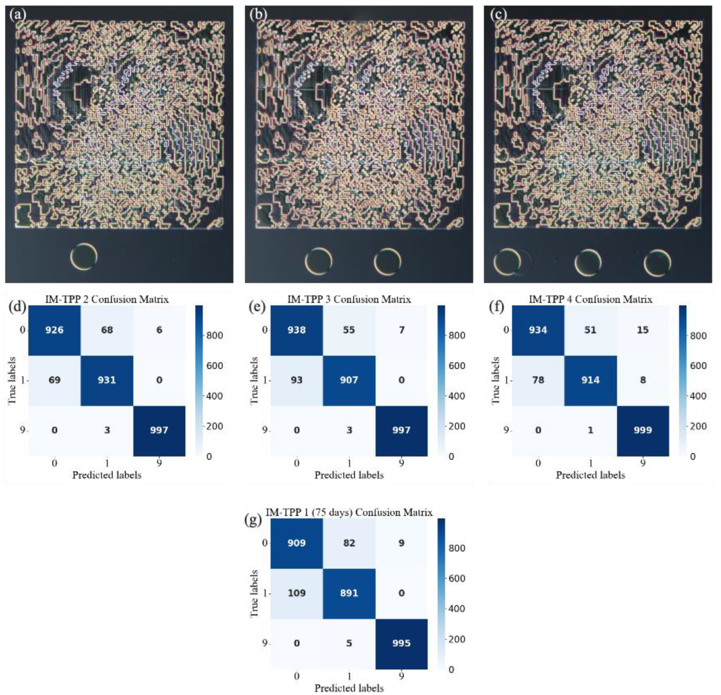
To validate the quality, stability, and consistency of the samples fabricated using the IM-TPP process, we applied the improved covering layer preparation procedure and reprocessed three new sample sets for comprehensive performance testing. The improved process uses 100 μm thick spacers in combination with quartz flat molds and ultraviolet single-photon curing (390–480 nm, 3000 mJ/cm
2) to precisely control the covering layer thickness, effectively reducing the impact of stitching gaps and fabrication errors. As shown in
Figure 6, the classification accuracy rates of the newly-prepared three groups of IM-TPP samples on the 3000 test sets were 95.13%, 94.73% and 94.90% respectively. The average value of the four samples before and after was 94.86%, which was highly consistent with the training result (95.43%) and the simulation prediction (95.03%). The standard deviation was only 0.18%, demonstrating excellent process consistency. These results indicate that the improved IM-TPP process not only significantly enhances the classification performance of individual samples but also ensures high-quality consistency across multiple batches. The UV curing process further reduced the impact of processing errors by eliminating stitching marks on the covering layer, providing a solid foundation for the large-scale production of high-precision DNNs.
We then performed repeatability validation on the first batch of IM-TPP samples (initial accuracy 94.67%). Under standard room conditions (20 °C, relative humidity 45 ± 5%) with no packaging, after 75 days of storage, the classification accuracy dropped to 93.17%, with a performance degradation of only 1.5%. We attribute this degradation to the unsealed covering layer, which exposed the structure to air and caused aging and deformation, particularly affecting the intensity distribution of the detectors for labels 0 (shirts) and 1 (pants), which in turn impacted classification performance. This aging effect is common in organic photoresists used in two-photon polymerization and does pose a challenge to long-term device stability. However, for short-term rapid prototyping, this process has demonstrated high-precision replication capability from simulation to experiment, and the limited performance degradation does not detract from its practical value in rapid validation scenarios.
This result suggests that environmental factors need further attention regarding long-term performance, but for short-term applications, the IM-TPP process still offers significant advantages. To address the aging of structures over time after photoresist curing, we believe that future improvements could involve using photoresists containing inorganic components to further enhance device stability. For instance, replacing IP-S with IP-G (which has the same refractive index but higher Young’s modulus and greater rigidity) or combining photoresists like GP-Silica with glass-based photoresists to fabricate the covering layer could improve the mechanical strength and aging resistance of the structures. Additionally, adding encapsulation protection would effectively shield the devices from environmental influences, slowing down the aging process. These improvements are expected to further optimize the long-term performance of the IM-TPP process in the future.
Precise phase control is crucial in optical neural networks, especially for complex classification tasks, as it directly determines the network’s ability to process information across different categories. The phase value of each pixel in the phase modulation layer governs the propagation characteristics of the optical field and the computational outcomes. Therefore, high-precision phase modulation is key to ensuring classification accuracy. Traditional TPP processes are limited by the lower modulation layer height (1.16 μm) and a larger refractive index difference (0.547), which lead to phase modulation errors and reduced classification accuracy. In contrast, the IM-TPP process increases the modulation layer height to 15.43 μm and reduces the refractive index difference to 0.041, significantly minimizing phase delay errors while relaxing the stringent requirements for pixel height uniformity. This design provides more refined phase modulation for each pixel, significantly improving the accuracy of optical field control and enhancing DNN classification performance.
However, the IM-TPP process still has certain limitations. For instance, the UV curing process in the covering layer preparation may result in incomplete local curing due to uneven photoresist absorption, affecting the flatness of the phase modulation layer. Additionally, the current process still needs optimization for large-area stitching, as small errors at the stitching boundaries may accumulate and amplify in ultra-large-scale DNNs. To address these issues, future improvements could involve introducing adaptive light intensity control techniques to optimize curing uniformity, based on the concept of refractive index matching. Furthermore, integrating real-time optical feedback systems to monitor stitching accuracy could further enhance the process’s robustness.
Both experimental and simulation results validate the significant advantages of IM-TPP, providing a more stable computational foundation for complex tasks. However, the suggested improvements will further enhance its potential for practical applications.
4. Conclusions and Discussion
In conclusion, the IM-TPP process enhances the fabrication precision of diffractive neural networks (DNNs) by reducing phase errors caused by substrate tilt and stitching inaccuracies, which are common in traditional two-photon polymerization (TPP). By utilizing refractive index matching with IP-Dip (1.547) and IP-S (1.506) photoresists, it achieves a small refractive index difference of 0.041—an optimized value that allows for a thicker phase modulation layer (15.43 μm). This improvement enhances phase control and increases robustness. Experimental results from the FashionMNIST task show a classification accuracy increase from 91.67% to 94.67%, approaching the simulated accuracy of 95.03%, with consistent performance across samples (94.86% average, 0.18% standard deviation). Additionally, simulations of the MNIST four-class task under tilt conditions demonstrate an accuracy improvement from 86.48% to 94.05%, underscoring IM-TPP’s effectiveness in mitigating fabrication errors and boosting DNN performance. These results establish IM-TPP as a reliable approach for rapid prototyping of high-precision optical computing devices.
The IM-TPP process overcomes a significant drawback of traditional TPP by reducing phase errors through refractive index optimization, delivering a reliable method for crafting high-precision optical neural networks. Its thicker modulation layer markedly lowers sensitivity to substrate tilt, evidenced by a decrease in phase delay differences (e.g., from 0.843π to 0.063π for a 0.2° tilt), ensuring consistent task performance. After 75 days of storage, the classification accuracy of unsealed samples decreased by 1.5%. Future optimization could focus on material improvements, such as replacing IP-S with IP-G—offering the same refractive index but enhanced rigidity and higher Young’s modulus—or employing glass-based photoresists like GP-Silica as the cover layer to enhance structural stability and long-term durability. Additionally, encapsulation can shield devices from environmental factors, slowing degradation and enhancing the long-term performance of IM-TPP-fabricated components.
Beyond these enhancements, the refractive index matching approach of IM-TPP provides valuable guidance for large-scale industrial micro-nano fabrication, offering a cost-effective means to minimize processing errors and support mass production of precise optical elements. Equally critical, IM-TPP ensures high-fidelity replication from simulation to experiment, aligning fabricated deep neural networks (DNNs) closely with theoretical designs. This precision is essential for advancing intelligent optical devices and expanding optical computing applications, solidifying IM-TPP’s role in driving innovation across micro-nano fabrication and beyond.
Author Contributions
Conceptualization, M.F., R.R. and Q.Z.; Methodology, M.F. and R.R.; Software, M.F. and X.M.; Formal Analysis, M.F. and X.M.; Validation, M.F.; Investigation, M.F. and R.R.; Resources, W.S.; Data Curation, M.F.; Writing—Original Draft Preparation, M.F.; Writing—Review & and Editing, M.F., R.R. and Q.Z.; Visualization, M.F.; Supervision, R.R. and Q.Z.; Project Administration, R.R. and Q.Z.; Funding Acquisition, W.S., Q.Z. and R.R. All authors have read and agreed to the published version of the manuscript.
Funding
This research was funded by the National Natural Science Foundation of China (Grant No. 12304400), the Teacher Professional Development Project—Shanghai Young Teacher Training Funding Project, the Shanghai Municipal Science and Technology Major Project, the Shanghai Frontiers Science Center Program (2021–2025 No. 20), the Shanghai Science and Technology Innovation Action Plan (Grant No. 23JC1403100 and No. 24JD1402700) and the Shanghai Pujiang Programme.
Institutional Review Board Statement
Not applicable.
Informed Consent Statement
Not applicable.
Data Availability Statement
The data presented in this study are available upon request from the corresponding author.
Acknowledgments
We thank Zhecheng Qiu for his helpful discussion in our project.
Conflicts of Interest
The authors declare no conflicts of interest. The funders had no role in the design of the study; in the collection, analyses, or interpretation of data; in the writing of the manuscript; or in the decision to publish the results.
Abbreviations
The following abbreviations are used in this manuscript:
| TPP | Two-photon polymerization |
| DNNs | Diffractive neural networks |
| IM-TPP | Index-matched two-photon polymerization |
| RID | Refractive index difference |
| FFT | Fast Fourier transform |
| BP | Backpropagation |
| SCE | SoftMax Cross Entropy |
| MSE | Mean Squared Error |
| SLM | Spatial light modulator |
| DMD | Digital micromirror devices |
References
- Lin, X.; Rivenson, Y.; Yardimci, N.T.; Veli, M.; Luo, Y.; Jarrahi, M.; Ozcan, A. All-optical machine learning using diffractive deep neural networks. Science 2018, 361, 1004–1008. [Google Scholar] [CrossRef] [PubMed]
- Li, H.; Li, F.; Li, X. Metasurface optical diffraction neural network and its applications (Invited). Laser Optoelectron. Prog. 2024, 61, 1913016. [Google Scholar]
- Luo, Y.; Mengu, D.; Yardimci, N.T.; Rivenson, Y.; Veli, M.; Jarrahi, M.; Ozcan, A. Design of task-specific optical systems using broadband diffractive neural networks. Light Sci. Appl. 2019, 8, 112. [Google Scholar] [CrossRef]
- Yan, T.; Wu, J.; Zhou, T.; Xie, H.; Xu, F.; Fan, J.; Fang, L.; Lin, X.; Dai, Q. Fourier-space Diffractive Deep Neural Network. Phys. Rev. Lett. 2019, 123, 023901. [Google Scholar] [CrossRef]
- Motz, G.A.; Doskolovich, L.L.; Soshnikov, D.V.; Byzov, E.V.; Bezus, E.A.; Golovastikov, N.V.; Bykov, D.A. Design of Diffractive Neural Networks for Solving Different Classification Problems at Different Wavelengths. Photonics 2024, 11, 780. [Google Scholar] [CrossRef]
- Zhou, J.; Pu, H.; Yan, J. Spatiotemporal diffractive deep neural networks. Opt. Express 2024, 32, 1864–1877. [Google Scholar] [CrossRef]
- Zheng, M.; Shi, L.; Zi, J. Optimize performance of a diffractive neural network by controlling the Fresnel number. Photonics Res. 2022, 10, 2667–2676. [Google Scholar] [CrossRef]
- Wang, Q.; Gu, M.; Zhang, Q.; Yu, H.; Huang, Z. Two-photon nanolithography of micrometer scale diffractive neural network with cubical diffraction neurons at the visible wavelength. Chin. Opt. Lett. 2024, 22, 102201. [Google Scholar] [CrossRef]
- Goi, E.; Schoenhardt, S.; Gu, M. Direct retrieval of Zernike-based pupil functions using integrated diffractive deep neural networks. Nat. Commun. 2022, 13, 7531. [Google Scholar] [CrossRef]
- Sun, Y.; Dong, M.; Yu, M.; Liu, X.; Zhu, L. Review of diffractive deep neural networks. J. Opt. Soc. Am. B 2023, 40, 2951–2961. [Google Scholar] [CrossRef]
- Chen, H.; Feng, J.; Jiang, M.; Wang, Y.; Lin, J.; Tan, J.; Jin, P. Diffractive Deep Neural Networks at Visible Wavelengths. Engineering 2021, 7, 1483–1491. [Google Scholar] [CrossRef]
- Amanatiadis, S.A.; Salonikios, V.; Nitas, M.; Zygiridis, T.; Kantartzis, N.V.; Yioultsis, T.V. Sensitivity Analysis of Metamaterial-Inspired SIW Focusing on Resonator Misalignment. IEEE Access 2024, 12, 63942–63949. [Google Scholar] [CrossRef]
- Dong, Y.; Lin, D.; Chen, L.; Li, B.; Chen, X.; Zhang, Q.; Luan, H.; Fang, X.; Gu, M. Compact eternal diffractive neural network chip for extreme environments. Commun. 2024, 3, 64. [Google Scholar] [CrossRef]
- O’Halloran, S.; Pandit, A.; Heise, A.; Kellett, A. Two-photon polymerization: Fundamentals, materials, and chemical modification strategies. Adv. Sci. 2023, 10, 2204072. [Google Scholar] [CrossRef]
- Jian, B.; Li, H.; He, X.; Wang, R.; Yang, H.; Ge, Q. Two-photon polymerization-based 4D printing and its applications. Int. J. Extrem. Manuf. 2023, 6, 012001. [Google Scholar] [CrossRef]
- Otuka, A.J.G.; Tomazio, N.B.; Paula, K.T.; Mendonça, C.R. Two-photon polymerization: Functionalized microstructures, micro-resonators, and bio-scaffolds. Polymers 2021, 13, 1994. [Google Scholar] [CrossRef] [PubMed]
- Correa, D.S.; Tayalia, P.; Cosendey, G.; dos Santos, D.S.; Aroca, R.F.; Mazur, E.; Mendonca, C.R. Two-photon polymerization for fabricating structures containing the biopolymer chitosan. J. Nanosci. Nanotechnol. 2009, 9, 5845–5849. [Google Scholar] [CrossRef]
- Guo, J.; Sun, T.; He, C.; Xia, J.; Cao, M.; Wang, C. Design and experimental investigation of nano-structured optical polarizing elements based on two-photon photopolymerization. In Proceedings of the Fourteenth National Conference on Laser Technology and Optoelectronics, Shanghai, China, 17–20 May 2019; Volume 11170, p. 1117015. [Google Scholar]
- Jia, E.; Xie, C.; Xiao, N.; Courvoisier, F.; Hu, M. Two-photon polymerization of femtosecond high-order Bessel beams with aberration correction. Chin. Opt. Lett. 2023, 21, 071203. [Google Scholar] [CrossRef]
- Wang, C.; Sun, S.; Qian, B.; Peng, S.; Feng, Z.; Qiu, J. Quantum-dot-based optical fiber temperature sensor fabricated by two-photon polymerization. Laser Optoelectron. Prog. 2024, 61, 2336001. [Google Scholar] [CrossRef]
- Geng, Q.; Wang, D.; Chen, P.; Chen, S.-C. Ultrafast multi-focus 3-D nano-fabrication based on two-photon polymerization. Nat. Commun. 2019, 10, 2179. [Google Scholar] [CrossRef]
- Kiefer, P.; Hahn, V.; Kalt, S.; Sun, Q.; Eggeler, Y.M.; Wegener, M. A multi-photon (7 × 7)-focus 3D laser printer based on a 3D-printed diffractive optical element and a 3D-printed multi-lens array. Light Adv. Manuf. 2024, 4, 28–41. [Google Scholar] [CrossRef]
- Wang, Z.; Wu, Y.L.; Chen, L.; Bakhtiyari, A.N.; Yu, W.; Qi, D.; Zheng, H. Spatial light assisted femtosecond laser direct writing of a bionic superhydrophobic Fresnel microlens arrays. Opt. Laser Technol. 2025, 180, 111451. [Google Scholar] [CrossRef]
- He, Z.; Chen, F.; He, S. Fabrication of microneedles using two-photon polymerization with low numerical aperture. Opt. Commun. 2024, 553, 130093. [Google Scholar] [CrossRef]
- Moughames, J.; Porte, X.; Thiel, M.; Ulliac, G.; Larger, L.; Jacquot, M.; Kadic, M.; Brunner, D. Three-dimensional waveguide interconnects for scalable integration of photonic neural networks. Optica 2020, 7, 640–646. [Google Scholar] [CrossRef]
- Farsari, M.; Chichkov, B. Two-photon fabrication. Nat. Photonics 2009, 3, 450–452. [Google Scholar] [CrossRef]
- Yu, H.; Huang, Z.; Lamon, S.; Wang, B.; Ding, H.; Lin, J.; Wang, Q.; Luan, H.; Gu, M.; Zhang, Q. All-optical image transportation through a multimode fibre using a miniaturized diffractive neural network on the distal facet. Nat. Photonics 2025. [Google Scholar] [CrossRef]
- Hu, J.; Liao, K.; Dinc, N.U.; Gigli, C.; Bai, B.; Gan, T.; Li, X.; Chen, H.; Yang, X.; Li, Y.; et al. Subwavelength imaging using a solid-immersion diffractive optical processor. eLight 2024, 4, 8. [Google Scholar] [CrossRef]
- Pan, X.; Zuo, H.; Bai, H.; Wu, Z.; Cui, X. Real-time wavefront correction using diffractive optical networks. Opt. Express 2023, 31, 1067–1078. [Google Scholar] [CrossRef] [PubMed]
- Song, Y.; Gui, C.; Huo, Z.; Lee, S.W.R.; Liu, S. Mechanical system and dynamic control in photolithography for nanoscale fabrication: A critical review. Int. J. Mech. Syst. Dyn. 2021, 1, 35–51. [Google Scholar] [CrossRef]
- Zhou, S.; Lu, Z.; Yuan, Q.; Wu, G.; Liu, C.; Liu, H.; Feng, L. Measurement and compensation of a stitching error in a DMD-based step-stitching photolithography system. Appl. Opt. 2021, 60, 9074–9081. [Google Scholar] [CrossRef]
- Xu, X.; Huang, Z.; Gao, T.; Wei, J. Analysis and compensation of alignment error in laser scanning heat-mode lithography system. Appl. Phys. B 2025, 131, 29. [Google Scholar] [CrossRef]
- Pretheesh Kumar, V.C.; Ganesan, A.R. Nano scale tilt measurement using a polarizing phase shifting cyclic interferometer. Opt. Laser Technol. 2019, 120, 105691. [Google Scholar] [CrossRef]
- Nguyen, P.-T.; Nguyen, T.K.C.; Hoang, H.H.; Vu, T.T.; Cao, X.B. Real–Time Automatic Laser Focusing System for High–Precision Micromachining by Image Processing. In Proceedings of the 2nd Annual International Conference on Material, Machines and Methods for Sustainable Development (MMMS2020), MMMS 2020, Nha Trang, Vietnam, 12–15 November 2020; Lecture Notes in Mechanical Engineering. Long, B.T., Kim, Y.H., Ishizaki, K., Toan, N.D., Parinov, I.A., Vu, N.P., Eds.; Springer: Berlin/Heidelberg, Germany, 2021. [Google Scholar] [CrossRef]
- Lee, J.-C.; Yang, S.-H. Development of nanopositioning mechanism with real-time compensation algorithm to improve the positional accuracy of a linear stage. Precis. Eng. 2017, 50, 328–336. [Google Scholar] [CrossRef]
- Cao, B.X.; Le, P.H.; Ahn, S.; Kang, H.; Kim, J.; Noh, J. Automatic real-time focus control system for laser processing using dynamic focusing optical system. Opt. Express 2017, 25, 28427–28441. [Google Scholar] [CrossRef]
- Fu, Y.; Su, Y.; Wei, J.; Wang, B.; Li, J. Auto-focusing femtosecond laser manufacturing system via acoustic emission technology. Opt. Lett. 2024, 49, 558–561. [Google Scholar] [CrossRef]
- Orange-Kedem, R.; Nehme, E.; Weiss, L.E.; Ferdman, B.; Alalouf, O.; Opatovski, N.; Shechtman, Y. 3D printing-based fabrication of diffractive optical elements by near-index-matching. In Proceedings of the Optica Design and Fabrication Congress 2023 (IODC, OFT), Québec, QC, Canada, 4–8 June 2023; Technical Digest Series. Optica Publishing Group: Washington DC, USA, 2023. paper OM3B.3. [Google Scholar]
| Disclaimer/Publisher’s Note: The statements, opinions and data contained in all publications are solely those of the individual author(s) and contributor(s) and not of MDPI and/or the editor(s). MDPI and/or the editor(s) disclaim responsibility for any injury to people or property resulting from any ideas, methods, instructions or products referred to in the content. |
© 2025 by the authors. Licensee MDPI, Basel, Switzerland. This article is an open access article distributed under the terms and conditions of the Creative Commons Attribution (CC BY) license (https://creativecommons.org/licenses/by/4.0/).

