Enhanced Localized Electric Field from Surface Plasmon Coupling in a Silver Nanostructure Array with a Silver Thin Film for Bioimaging and Biosensing


Abstract

1. Introduction
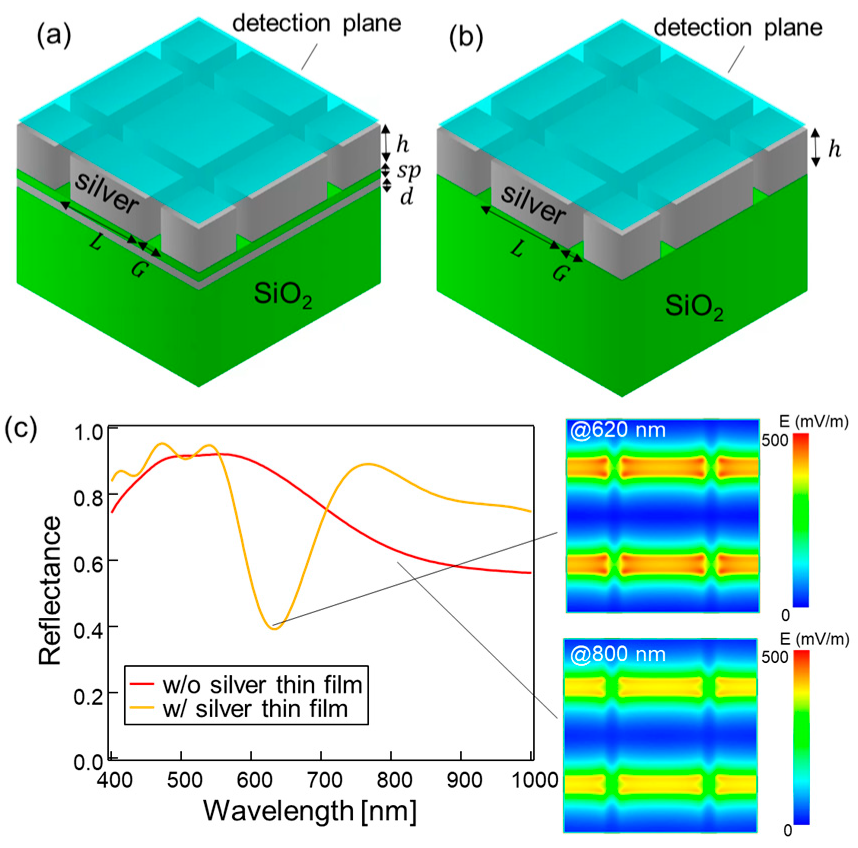
2. Methods
3. Results and Discussions
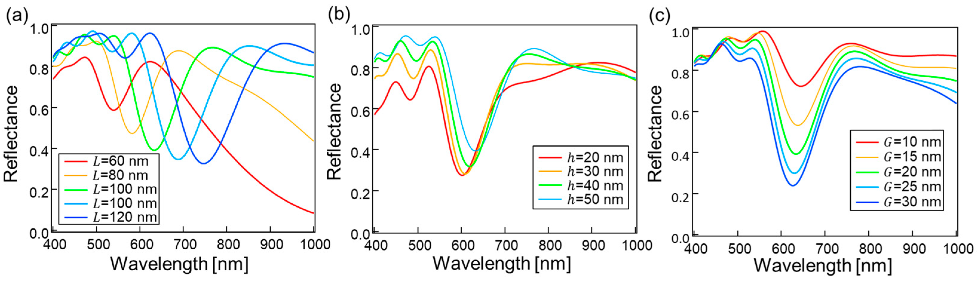
3.1. Resonance Peak Tuning via Structural Parameters
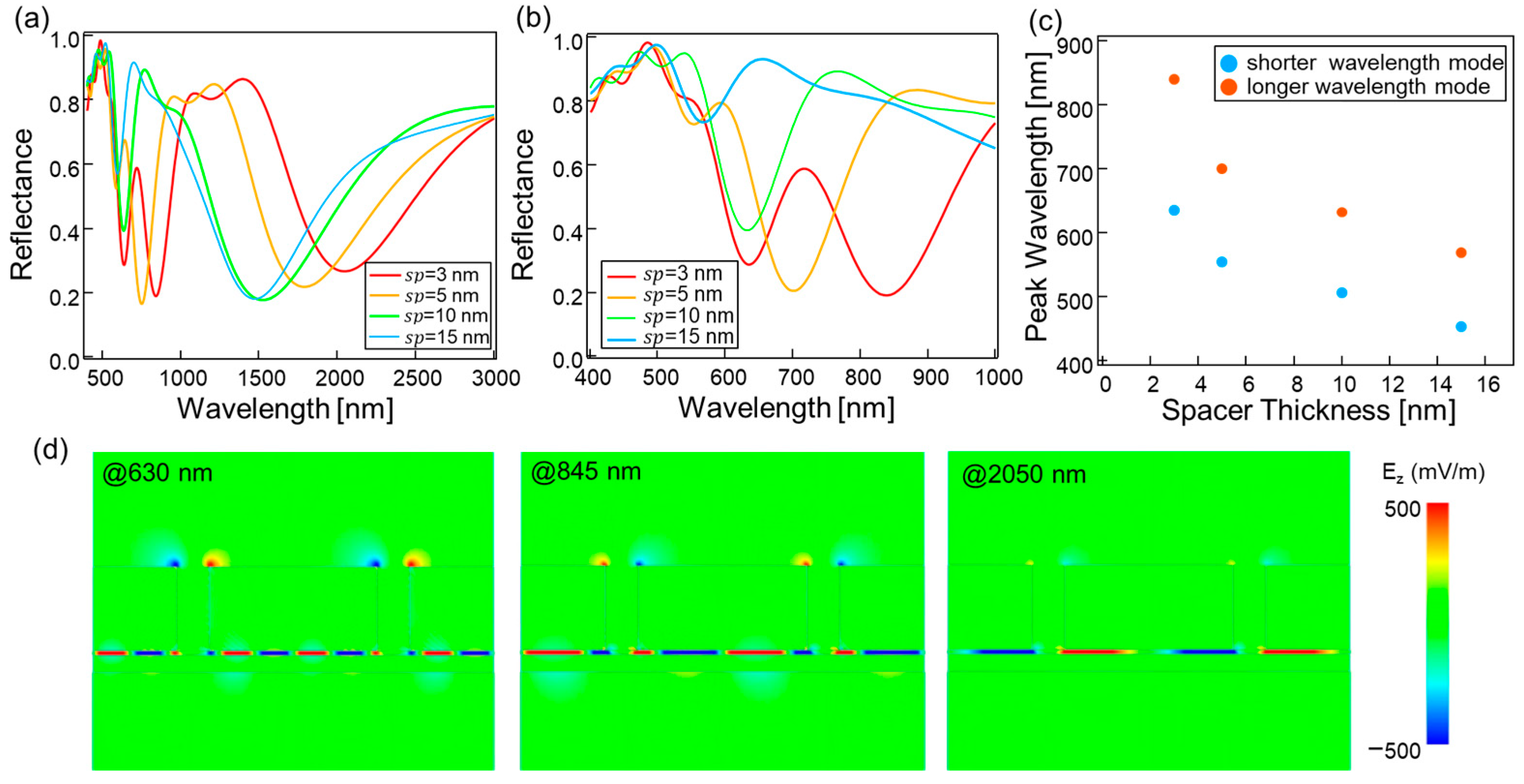
3.2. Mode Analysis Through Spacer Layer Thickness
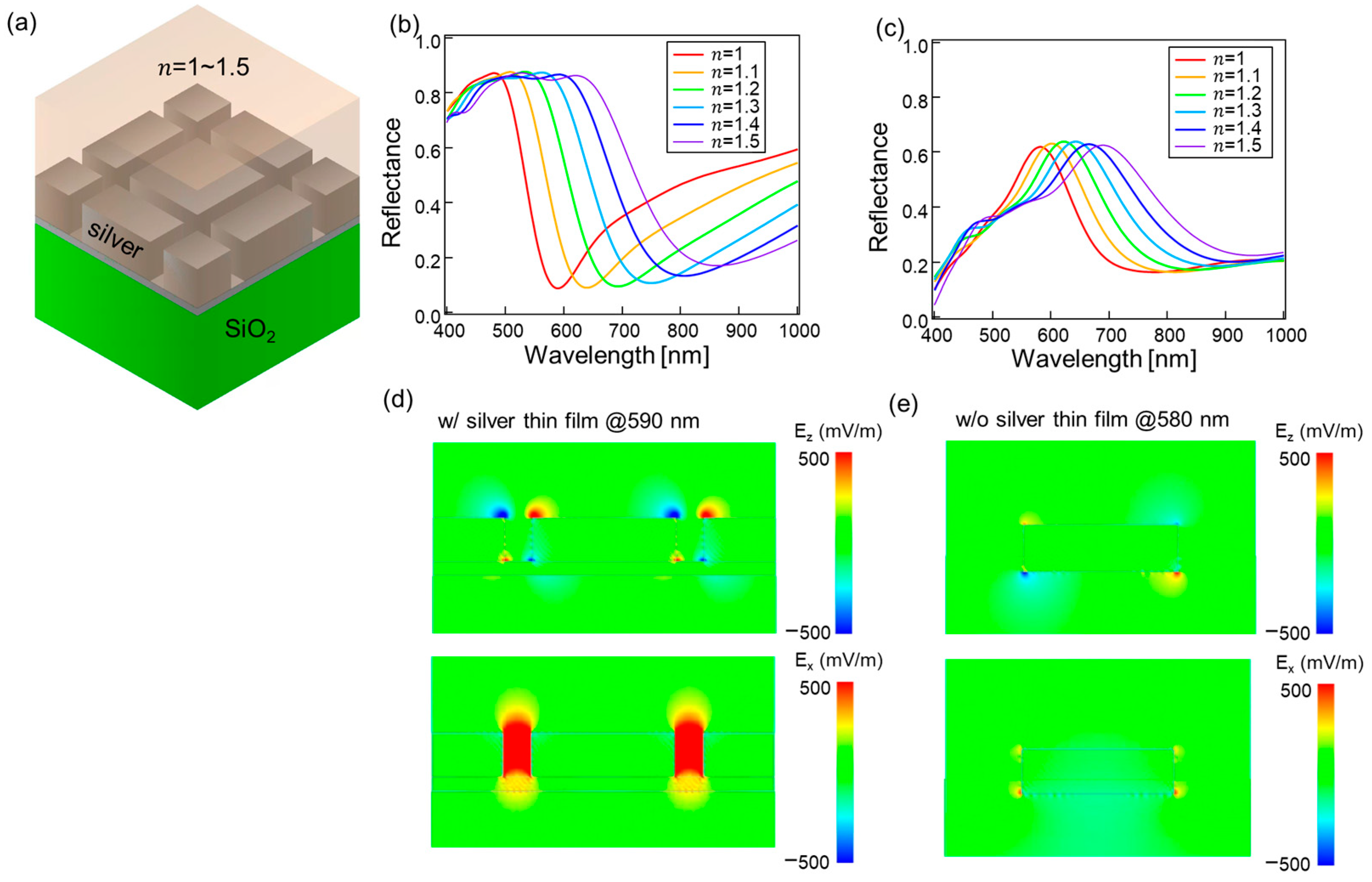
3.3. Evaluation of Refractive Index Sensitivity
4. Conclusions
Author Contributions
Funding
Institutional Review Board Statement
Informed Consent Statement
Data Availability Statement
Conflicts of Interest
References
- Li, L.; Chen, F. Tunable four-band metamaterial absorber and sensor based on a stacking double-ring Dirac semimetal structure design. Phys. Lett. A 2025, 544, 130489. [Google Scholar] [CrossRef]
- Prutphongs, P.; Aoki, K.; Ito, R.; Hara, M.; Ikezawa, S.; Iwami, K. Highly efficient multifunctional metasurface integrating lens, prism, and wave plate. Opt. Express 2024, 32, 28599–28610. [Google Scholar] [CrossRef] [PubMed]
- Gao, W.; Chen, F.; Yang, W. Modulator and sensor based on in-plane mode weak coupling in borophene metamaterial. Photon. Nanostruct. Fundam. Appl. 2025, 63, 101366. [Google Scholar] [CrossRef]
- Aydin, K.; Ferry, V.E.; Briggs, R.M.; Atwater, H.A. Broadband polarization-independent resonant light absorption using ultrathin plasmonic super absorbers. Nat. Commun. 2011, 2, 517. [Google Scholar] [CrossRef]
- Hedayati, M.K.; Zillohu, A.U.; Strunskus, T.; Faupel, F.; Elbahri, M. Plasmonic tunable metamaterial absorber as ultraviolet protection film. Appl. Phys. Lett. 2014, 104, 041103. [Google Scholar] [CrossRef]
- Zhang, Y.; Barhoumi, A.; Lassiter, J.B.; Halas, N.J. Orientation-Preserving Transfer and Directional Light Scattering from Individual Light-Bending Nanoparticles. Nano Lett. 2011, 11, 1838–1844. [Google Scholar] [CrossRef]
- Nien, L.-W.; Lin, S.-C.; Chao, B.-K.; Chen, M.-J.; Li, J.-H.; Hsueh, C.-H. Giant Electric Field Enhancement and Localized Surface Plasmon Resonance by Optimizing Contour Bowtie Nanoantennas. J. Phys. Chem. C 2013, 117, 25004–25011. [Google Scholar] [CrossRef]
- Abdulhalim, I. Coupling configurations between extended surface electromagnetic waves and localized surface plasmons for ultrahigh field enhancement. Nanophotonics 2018, 7, 1891–1916. [Google Scholar] [CrossRef]
- Cathcart, N.; Chen, J.I.L.; Kitaev, V. LSPR Tuning from 470 to 800 nm and Improved Stability of Au–Ag Nanoparticles Formed by Gold Deposition and Rebuilding in the Presence of Poly(styrenesulfonate). Langmuir 2018, 34, 612–621. [Google Scholar] [CrossRef]
- Chang, H.-H.; Murphy, C.J. Mini Gold Nanorods with Tunable Plasmonic Peaks beyond 1000 nm. Chem. Mater. 2018, 30, 1427–1435. [Google Scholar] [CrossRef]
- Yizhao, P.; Fang, C.; Yuchang, L.; Wenxing, Y.; Zao, Y.; Shaolin, K. Coherent coupling of localized surface plasmons and surface plasmons in borophene-based metamaterial. Micro Nano Struct. 2024, 194, 207941. [Google Scholar] [CrossRef]
- Huang, L.; Maerkl, S.J.; Martin, O.J.F. Integration of plasmonic trapping in a microfluidic environment. Opt. Express 2009, 17, 6018–6024. [Google Scholar] [CrossRef] [PubMed]
- Devilez, A.; Stout, B.; Bonod, N. Compact Metallo-Dielectric Optical Antenna for Ultra Directional and Enhanced Radiative Emission. ACS Nano 2010, 4, 3390–3396. [Google Scholar] [CrossRef] [PubMed]
- Chirumamilla, M.; Toma, A.; Gopalakrishnan, A.; Das, G.; Zaccaria, R.P.; Krahne, R.; Rondanina, E.; Leoncini, M.; Liberale, C.; De Angelis, F.; et al. 3D Nanostar Dimers with a Sub-10-nm Gap for Single-/Few-Molecule Surface-Enhanced Raman Scattering. Adv. Mater. 2014, 26, 2353–2358. [Google Scholar] [CrossRef]
- Hatab, N.A.; Hsueh, C.-H.; Gaddis, A.L.; Retterer, S.T.; Li, J.-H.; Eres, G.; Zhang, Z.; Gu, B. Free-Standing Optical Gold Bowtie Nanoantenna with Variable Gap Size for Enhanced Raman Spectroscopy. Nano Lett. 2010, 10, 4952–4955. [Google Scholar] [CrossRef]
- Badshah, M.A.; Kim, J.; Jang, H.; Kim, S.-M. Fabrication of Highly Packed Plasmonic Nanolens Array Using Polymer Nanoimprinted Nanodots for an Enhanced Fluorescence Substrate. Polymers 2018, 10, 649. [Google Scholar] [CrossRef]
- Li, W.-D.; Ding, F.; Hu, J.; Chou, S.Y. Three-dimensional cavity nanoantenna coupled plasmonic nanodots for ultrahigh and uniform surface-enhanced Raman scattering over large area. Opt. Express 2011, 19, 3925–3936. [Google Scholar] [CrossRef]
- Chang, C.C.; Wu, H.L.; Kuo, C.H.; Huang, M.H. Hydrothermal Synthesis of Monodispersed Octahedral Gold Nanocrystals with Five Different Size Ranges and Their Self-Assembled Structures. Chem. Mater. 2008, 20, 7570–7574. [Google Scholar] [CrossRef]
- Gong, J.; Li, G.; Tang, Z. Self-assembly of noble metal nanocrystals: Fabrication, optical property, and application. Nano Today 2012, 7, 564–585. [Google Scholar] [CrossRef]
- Lu, J.; Xue, Y.; Bernardino, K.; Zhang, N.-N.; Gomes, W.R.; Ramesar, N.S.; Liu, S.; Hu, Z.; Sun, T.; de Moura, A.F.; et al. Enhanced optical asymmetry in supramolecular chiroplasmonic assemblies with long-range order. Science 2021, 371, 1368–1374. [Google Scholar] [CrossRef]
- Zhang, Q.; Li, W.; Wen, L.-P.; Chen, J.; Xia, Y. Facile Synthesis of Ag Nanocubes of 30 to 70 nm in Edge Length with CF3COOAg as a Precursor. Chem. Eur. J. 2010, 16, 10234–10239. [Google Scholar] [CrossRef] [PubMed]
- Agrawal, H.; Garnett, E.C. Nanocube Imprint Lithography. ACS Nano 2020, 14, 11009–11016. [Google Scholar] [CrossRef]
- Melli, M.; Polyakov, A.; Gargas, D.; Huynh, C.; Scipioni, L.; Bao, W.; Ogletree, D.F.; Schuck, P.J.; Cabrini, S.; Weber-Bargioni, A. Reaching the Theoretical Resonance Quality Factor Limit in Coaxial Plasmonic Nanoresonators Fabricated by Helium Ion Lithography. Nano Lett. 2013, 13, 2687–2691. [Google Scholar] [CrossRef] [PubMed]
- Liu, H.-W.; Lin, F.-C.; Lin, S.-W.; Wu, J.-Y.; Chou, B.-T.; Lai, K.-J.; Lin, S.-D.; Huang, J.-S. Single-Crystalline Aluminum Nanostructures on a Semiconducting GaAs Substrate for Ultraviolet to Near-Infrared Plasmonics. ACS Nano 2015, 9, 3875–3886. [Google Scholar] [CrossRef]
- Haes, A.J.; Chang, L.; Klein, W.L.; Van Duyne, R.P. Detection of a Biomarker for Alzheimer’s Disease from Synthetic and Clinical Samples Using a Nanoscale Optical Biosensor. J. Am. Chem. Soc. 2005, 127, 2264–2271. [Google Scholar] [CrossRef] [PubMed]
- Wang, X.; Li, Y.; Wang, H.; Fu, Q.; Peng, J.; Wang, Y.; Du, J.; Zhou, Y.; Zhan, L. Gold nanorod-based localized surface plasmon resonance biosensor for sensitive detection of hepatitis B virus in buffer, blood serum and plasma. Biosens. Bioelectron. 2010, 26, 404–410. [Google Scholar] [CrossRef]
- Titus, E.J.; Willets, K.A. Superlocalization Surface-Enhanced Raman Scattering Microscopy: Comparing Point Spread Function Models in the Ensemble and Single-Molecule Limits. ACS Nano 2013, 7, 8284–8294. [Google Scholar] [CrossRef]
- Masuda, S.; Yanase, Y.; Usukura, E.; Ryuzaki, S.; Wang, P.; Okamoto, K.; Kuboki, T.; Kidoaki, S.; Tamada, K. High-resolution imaging of a cell-attached nanointerface using a gold-nanoparticle two-dimensional sheet. Sci. Rep. 2017, 7, 3720. [Google Scholar] [CrossRef]
- Wu, Y.; Ali, M.R.K.; Chen, K.; Fang, N.; El-Sayed, M.A. Gold nanoparticles in biological optical imaging. Nano Today 2019, 24, 120–140. [Google Scholar] [CrossRef]
- Guo, X. Surface plasmon resonance based biosensor technique:A review. J. Biophotonics 2012, 5, 483–501. [Google Scholar] [CrossRef]
- Okamoto, K.; Okura, K.; Wang, P.; Ryuzaki, S.; Tamada, K. Flexibly tunable surface plasmon resonance by strong mode coupling using a random metal nanohemisphere on mirror. Nanophotonics 2020, 9, 3409–3418. [Google Scholar] [CrossRef]
- Hatsuoka, R.; Yamasaki, K.; Wada, K.; Matsuyama, T.; Okamoto, K. Tunable Plasmon Resonance in Silver Nanodisk-on-Mirror Structures and Scattering Enhancement by Annealing. Nanomaterials 2024, 14, 1559. [Google Scholar] [CrossRef] [PubMed]
- Tokimori, S.; Funato, K.; Wada, K.; Matsuyama, T.; Okamoto, K. Emission Enhancement of ZnO Thin Films in Ultraviolet Wavelength Region Using Au Nano-Hemisphere on Al Mirror Structures. Nanomaterials 2025, 15, 400. [Google Scholar] [CrossRef] [PubMed]
- Li, J.; Gan, R.; Guo, Q.; Liu, H.; Xu, J.; Yi, F. Tailoring optical responses of infrared plasmonic metamaterial absorbers by optical phonons. Opt. Express 2018, 26, 16769–16781. [Google Scholar] [CrossRef]
- Chang, C.-Y.; Lin, H.-T.; Lai, M.-S.; Shieh, T.-Y.; Peng, C.-C.; Shih, M.-H.; Tung, Y.-C. Flexible Localized Surface Plasmon Resonance Sensor with Metal–Insulator–Metal Nanodisks on PDMS Substrate. Sci. Rep. 2018, 8, 11812. [Google Scholar] [CrossRef]
- Zhang, C.; Hugonin, J.-P.; Greffet, J.-J.; Sauvan, C. Surface Plasmon Polaritons Emission with Nanopatch Antennas: Enhancement by Means of Mode Hybridization. ACS Photonics 2019, 6, 2788–2796. [Google Scholar] [CrossRef]
- Okamoto, K.; Tanaka, D.; Matsuyama, T.; Wada, K.; Arima, Y.; Tamada, K. Design and Optimization of Silver Nanostructured Arrays in Plasmonic Metamaterials for Sensitive Imaging Applications. Photonics 2024, 11, 292. [Google Scholar] [CrossRef]
- Wang, Y.-W.; Kao, K.-C.; Wang, J.-K.; Mou, C.-Y. Large-Scale Uniform Two-Dimensional Hexagonal Arrays of Gold Nanoparticles Templated from Mesoporous Silica Film for Surface-Enhanced Raman Spectroscopy. J. Phys. Chem. C 2016, 120, 24382–24388. [Google Scholar] [CrossRef]
- Vial, S.; Pastoriza-Santos, I.; Pérez-Juste, J.; Liz-Marzán, L.M. Plasmon Coupling in Layer-by-Layer Assembled Gold Nanorod Films. Langmuir 2007, 23, 4606–4611. [Google Scholar] [CrossRef]
- Liz-Marzán, L.M. Tailoring Surface Plasmons through the Morphology and Assembly of Metal Nanoparticles. Langmuir 2006, 22, 32–41. [Google Scholar] [CrossRef]
- Rakić, A.D.; Djurišsić, A.B.; Elazar, J.M.; Majewski, M.L. Optical properties of metallic films for vertical-cavity optoelectronic devices. Appl. Opt. 1998, 37, 5271–5283. [Google Scholar] [CrossRef] [PubMed]
- Yamasaki, K.; Ozawa, M.; Hatsuoka, R.; Matsuyama, T.; Wada, K.; Okamoto, K. Effect of thermal annealing on the surface plasmon properties of gold and silver nanodisk structures fabricated by electron beam lithography. Opt. Mater. Express 2024, 14, 1349–1350. [Google Scholar] [CrossRef]
- Aćimović, S.S.; Kreuzer, M.P.; González, M.U.; Quidant, R. Plasmon near-field coupling in metal dimers as a step toward single-molecule sensing. ACS Nano 2009, 3, 1231–1237. [Google Scholar] [CrossRef] [PubMed]
- Huang, Y.; Ma, L.; Hou, M.; Li, J.; Xie, Z.; Zhang, Z. Hybridized plasmon modes and near-field enhancement of metallic nanoparticle-dimer on a mirror. Sci. Rep. 2016, 6, 30011. [Google Scholar] [CrossRef]
- Domina, K.L.; Khardikov, V.V.; Goryashko, V.; Nikitin, A.Y. Bonding and Antibonding Modes in Metal–Dielectric–Metal Plasmonic Antennas for Dual-Band Applications. Adv. Opt. Mater. 2020, 8, 1900942. [Google Scholar] [CrossRef]
- Schider, G.; Krenn, J.R.; Hohenau, A.; Ditlbacher, H.; Leitner, A.; Aussenegg, F.R.; Schaich, W.L.; Puscasu, I.; Monacelli, B.; Boreman, G. Plasmon dispersion relation of Au and Ag nanowires. Phys. Rev. B Condens. Matter. 2003, 68, 155427. [Google Scholar] [CrossRef]
- Nicoletti, O.; Wubs, M.; Mortensen, N.A.; Sigle, W.; van Aken, P.A.; Midgley, P.A. Surface plasmon modes of a single silver nanorod: An electron energy loss study. Opt. Express 2011, 19, 15371–15379. [Google Scholar] [CrossRef]
- Taghvaee, H.; Liu, F.; Diáz-Rubio, A.; Tretyakov, S. Subwavelength focusing by engineered power-flow conformal metamirrors. Phys. Rev. B 2021, 104, A90. [Google Scholar] [CrossRef]
- Kim, J.H.; Lee, J.Y.; Kim, E.S.; Jeong, M.Y. Electric field enhancement of coupled plasmonic nanostructures for optical amplification. PhotoniX 2023, 4, 8. [Google Scholar] [CrossRef]
- Liu, D.; Xue, C. Plasmonic Coupling Architectures for Enhanced Photocatalysis. Adv. Mater. 2021, 33, 2005738. [Google Scholar] [CrossRef]
- Chen, H.; Kou, X.; Yang, Z.; Ni, W.; Wang, J. Shape- and Size-Dependent Refractive Index Sensitivity of Gold Nanoparticles. Langmuir 2008, 24, 5233–5237. [Google Scholar] [CrossRef] [PubMed]
- Miller, M.M.; Lazarides, A.A. Sensitivity of Metal Nanoparticle Surface Plasmon Resonance to the Dielectric Environment. J. Phys. Chem. B 2005, 109, 21556–21565. [Google Scholar] [CrossRef] [PubMed]
- Finco, G.; Bideskan, M.Z.; Vertchenko, L.; Beliaev, L.Y.; Malureanu, R.; Lindvold, L.R.; Takayama, O.; Andersen, P.E.; Lavrinenk, A.V. Guided-mode resonance on pedestal and half-buried high-contrast gratings for biosensing applications. Nanophotonics 2021, 10, 4289–4296. [Google Scholar] [CrossRef]
- Zhang, Z.; Luo, L.; Xue, C.; Zhang, W.; Yan, S. Fano Resonance Based on Metal-Insulator-Metal Waveguide-Coupled Double Rectangular Cavities for Plasmonic Nanosensors. Sensors 2016, 16, 642. [Google Scholar] [CrossRef]
- Danaie, M.; Shahzadi, A. Design of a High-Resolution Metal–Insulator–Metal Plasmonic Refractive Index Sensor Based on a Ring-Shaped Si Resonator. Plasmonics 2019, 14, 1453–1465. [Google Scholar] [CrossRef]
- Duffett, G.; Wirth, R.; Rayer, M.; Martins, E.R.; Krauss, T.F. Metal-insulator-metal nanoresonators—Strongly confined modes for high surface sensitivity. Nanophotonics 2020, 9, 1547–1552. [Google Scholar] [CrossRef]
- Fahmy, H.M.; Mosleh, A.M.; Elghany, A.A.; Shams-Eldin, E.; Abu Serea, E.S.; Ali, S.A.; Shalan, A.E. Coated silver nanoparticles: Synthesis, cytotoxicity, and optical properties. RSC Adv. 2019, 9, 20118–20136. [Google Scholar] [CrossRef]

Disclaimer/Publisher’s Note: The statements, opinions and data contained in all publications are solely those of the individual author(s) and contributor(s) and not of MDPI and/or the editor(s). MDPI and/or the editor(s) disclaim responsibility for any injury to people or property resulting from any ideas, methods, instructions or products referred to in the content. |
© 2025 by the authors. Licensee MDPI, Basel, Switzerland. This article is an open access article distributed under the terms and conditions of the Creative Commons Attribution (CC BY) license (https://creativecommons.org/licenses/by/4.0/).
Share and Cite
Yamasaki, K.; Hatsuoka, R.; Wada, K.; Matsuyama, T.; Okamoto, K. Enhanced Localized Electric Field from Surface Plasmon Coupling in a Silver Nanostructure Array with a Silver Thin Film for Bioimaging and Biosensing. Photonics 2025, 12, 439. https://doi.org/10.3390/photonics12050439
Yamasaki K, Hatsuoka R, Wada K, Matsuyama T, Okamoto K. Enhanced Localized Electric Field from Surface Plasmon Coupling in a Silver Nanostructure Array with a Silver Thin Film for Bioimaging and Biosensing. Photonics. 2025; 12(5):439. https://doi.org/10.3390/photonics12050439
Chicago/Turabian StyleYamasaki, Kota, Ryohei Hatsuoka, Kenji Wada, Tetsuya Matsuyama, and Koichi Okamoto. 2025. "Enhanced Localized Electric Field from Surface Plasmon Coupling in a Silver Nanostructure Array with a Silver Thin Film for Bioimaging and Biosensing" Photonics 12, no. 5: 439. https://doi.org/10.3390/photonics12050439
APA StyleYamasaki, K., Hatsuoka, R., Wada, K., Matsuyama, T., & Okamoto, K. (2025). Enhanced Localized Electric Field from Surface Plasmon Coupling in a Silver Nanostructure Array with a Silver Thin Film for Bioimaging and Biosensing. Photonics, 12(5), 439. https://doi.org/10.3390/photonics12050439