Article

Constructing a Micro-Raman Spectrometer with Industrial-Grade CMOS Camera—High Resolution and Sensitivity at Low Cost

Center for Advanced Laser Techniques, Institute of Physics, Bijenička 46, 10000 Zagreb, Croatia
*
Author to whom correspondence should be addressed.
Photonics 2025, 12(4), 389; https://doi.org/10.3390/photonics12040389
Submission received: 11 March 2025 / Revised: 10 April 2025 / Accepted: 11 April 2025 / Published: 16 April 2025
(This article belongs to the Special Issue Research, Development and Application of Raman Scattering Technology)

Abstract

Until now, achieving both a high spectral resolution on the order of a few wavenumbers and the highest sensitivity in Raman scattering spectroscopy has required reliance on high-end laboratory instruments. Here, we introduce an innovative yet design-wise simple alternative: a cost-effective and compact micro-Raman spectrometer (µRS) that combines exceptional spectral resolution and sensitivity. Leveraging industrial-grade CMOS cameras and high-quality photographic objectives, our µRS maintains a footprint at least five times smaller than traditional lab-based spectrometers. Through detailed characterization and direct experimental comparison, which includes the use of calcite as a Raman standard, we demonstrate that our µRS achieves a spectral resolution of down to 2.5 cm−1. Using a single-layer MoS2 sample, we found that the sensitivity of our system, while somewhat lower, remains within a useful range compared to commercial research-grade confocal Raman microscopy systems. This study presents a compelling solution for researchers seeking efficient and high-resolution Raman spectroscopy tools across diverse applications, particularly in resource-limited or field-based settings.

1. Introduction

Raman spectrometers have become essential equipment not only in research laboratories, but also in industrial settings. Portable versions of these instruments enable the reliable in situ and on-site analysis of many (bio)chemicals, finding applications in fields such as forensic science, pharmaceuticals, healthcare, agriculture, and environmental monitoring.
Depending on the specific need and application, there is a wide range of Raman spectrometers to choose from. Among the most common types found in research labs are Research-Grade Raman Spectrometers (RGRSs) and Fiber Raman Spectrometers (FRSs).
FRSs are compact, robust, and relatively immune to stray light and external noise, making them ideal for in-field measurements and portable applications. However, their design prioritizes ease of use and mobility over a high spectral performance. Research-grade Raman spectrometers (RGRSs), on the other hand, offer higher spectral resolution and sensitivity, but are significantly more expensive—often costing several times more than FRSs—and are typically limited to benchtop formats, restricting their use to laboratory environments.
FRSs generally provide a spectral resolution in the 4–10 cm−1 range, which is sufficient for the quick, non-destructive identification of the chemical composition. However, for applications requiring a higher spectral resolution, such as distinguishing subtle peak shifts in solid-state physics or monitoring closely spaced vibrational modes, more advanced instrumentation is required. This need motivated us to develop a compact micro-Raman spectrometer (µRS) from scratch, aiming to bridge the gap between the FRS portability and RGRS performance.
The aim of this paper is to demonstrate that a low-cost micro-Raman spectrometer (µRS) can be constructed using commercial off-the-shelf (COTS) components—such as photographic lenses, industrial CMOS cameras, and other widely available optical elements—while achieving spectral resolution and sensitivity that approach those of RGRSs. The result is a system that costs an order of magnitude less than a typical lab-grade Raman spectrometer. A detailed cost comparison is provided in Section S1 of the Supplementary Material (SM): Tables S2 and S3, highlighting the affordability of µRS. It should be noted that the term ‘micro-Raman’ in µRS refers specifically to the sub-micron laser excitation spot size, allowing Raman spectroscopy from micrometer-scale sample volumes. However, this system does not currently provide direct optical or chemical imaging (i.e., Raman mapping) functionality.
A high spectral resolution (i.e., <4 cm−1) and high sensitivity, up to now achievable only with RGRSs, are essential requirements for many Raman spectroscopy applications. For instance, a high spectral resolution in the order of a few wavenumbers is needed to monitor tiny changes in the Raman shift and linewidth of a Raman band, which provides insights into the local environment of a vibrating group. This is crucial for the development and research of low-dimensional materials such as monolayer MoS2 [1], to identify crystallinity [2,3], polymorphism [4,5], intrinsic stress or strain in solid state matter [6], hydrogen bonding [7], and protein folding in soft matter [8].
Achieving high sensitivity is equally important, as Raman scattering has a cross-section that is 10–12 orders of magnitude smaller than that of molecular absorption [9]. Thus, every photon is important, and a high-sensitivity spectrometer is necessary to obtain a sufficiently high signal-to-noise ratio (SNR) for low-light conditions. This is achieved through the combination of a high-throughput optical bench and a photon detector having low dark noise (DN) and high quantum efficiency (Qe) at the wavelengths of interest. More precisely, to obtain a good SNR, the detector needs to have Qe over the DN ratio (Qe/DN), as high as possible at the wavelengths of interest [10]. Let us first consider the optical bench throughput (OBT) contribution.
RGRSs simultaneously offer a high spectral resolution of <4 cm−1 and the highest sensitivity available on the market. Surprisingly, the OBT of a general purpose RGRS is sometimes lower than 40% [11,12]. As this type of Raman spectrometer is designed with excitation wavelength versatility and simplicity of use in mind, usually the same optical elements need to handle wavelengths spanning from the ultraviolet to the near infrared region (NIR). However, the broadband performance comes at the expense of the OBT. Therefore, we decided to limit our spectrometer’s spectral range to the visible region (VIS) where optical elements are abundant and come with a reasonable price tag.
Instead of mirrors or simple lenses, we have chosen general purpose photographic objectives. That was motivated by three reasons: they have a high transmittance of >95% throughout the whole VIS region, they are corrected for all major optical aberrations, and their cost is comparable to the cost of a simple achromatic lens from an optics laboratory supplier. By opting for a lens-based design, the optical grating reflectance becomes the limiting factor of the OBT. The only drawback is that the excitation wavelength is now limited to the VIS, but this is acceptable for many applications. An extension to the shorter end of the NIR (780–1050 nm), a spectral range that covers popular Raman excitation at 785 nm and that is still detectable with a low-cost silicon-based camera, is easily implemented simply by switching to grating and lenses optimized for this spectral region.
With the emergence of newer technology, particularly CMOS sensors, which are widely implemented in high-volume consumer electronics such as cell phones, CMOS imaging sensors have rapidly gained popularity in industrial, large-scale, and cost-effective research applications [13]. These sensors have evolved to offer low DN and high Qe, making them a viable alternative to more expensive scientific-grade detectors. To achieve optimal sensitivity while minimizing costs, we selected two industrial-grade CMOS cameras (iCMOS), which provide a low read noise of 2–3 e/pixel, Qe greater than 60%, and a low dark current even without cooling [14]. These cameras offer a cost roughly one-tenth that of scientific-grade CCD or CMOS cameras, making them an attractive choice for high-performance yet affordable Raman spectroscopy.
We employ two different iCMOS cameras not only because they have different pixel pitches but also to investigate whether spectral resolution is limited by the pixel broadening effect. By comparing the two detectors, we aim to determine whether decreasing spectral dispersion per pixel leads to a tangible improvement in spectral resolution or whether the limiting factor lies elsewhere in the optical system. This dual-camera approach ensures a balance between cost, sensitivity, and spectral performance, making it a practical solution for high-resolution Raman spectroscopy.
Ma and coworkers compared a scientific CMOS (sCMOS) camera with an iCMOS camera (based on the IMX265 sensor, the same one as in CAM−L—the 3.45 µm pixel camera) and found that the SNR in low-light conditions is comparable and that the iCMOS camera even outperforms Electron-Multiplying CCDs (EMCCDs) for signals above 20 photons/pixel [15]. As a rule of thumb, for exposure times of less than a few seconds, iCMOS cameras offer a comparable performance to cooled sCMOS and sCCD cameras in terms of the negligible dark current noise contribution, and they do not require cooling [10,16,17]. Our primary motivation for building the µRS is to create a workhorse for confocal Raman mapping, an experimental technique that commonly uses exposure of less than 1 s. Therefore, it is reasonable to assume that for our experimental conditions, the dark noise of the CMOS camera is mainly due to the read noise, while the contribution of the dark current noise is negligible. Our experience shows that even longer exposures of 10–20 s give good results.

2. Micro-Raman Spectrometer Construction

A schematic of the µRS setup, illustrating all optical components along the beam path—from the excitation laser to the detector—is presented in Figure 1. The system consists of two main parts: the Raman probe, which focuses the 532 nm laser onto the sample, collects the Raman-scattered photons, and directs them to the entrance slit of the high-resolution spectrometer, and the lens-based dispersive spectrometer, which utilizes an iCMOS camera as the detector. A general overview of the device is provided here, while detailed specifications, including exact part numbers and component choices, are given in Section S1 in the SM.

2.1. Micro-Raman Probe

For the excitation laser L (Figure 1), we selected a single longitudinal mode (SLM) diode-pumped solid-state (DPSS) laser operating at 532.13 nm. The laser spectrum and its linewidth ( Δ ν ~ L = 0.4 cm−1) were characterized using an optical spectrum analyzer (OSA) in high-resolution mode (Section S2 in the SM: Figure S2).
In Raman spectroscopy, the natural linewidth Γ of a Raman peak is affected by both the spectrometer’s spectral resolution Δ ν ~ S and the laser linewidth Δ ν ~ L . The experimentally measured linewidth Δ ν ~ M represents a convolution of these broadening effects. However, since Δ ν ~ S of the µRS is, as we will see in the following, at least five times broader than Δ ν ~ L , the contribution of Δ ν ~ L to Δ ν ~ M is negligible in our measurements.
The excitation beam first passes through the beam expander BE (Figure 1), where it is expanded fivefold before being reflected by the folding mirror M (Figure 1). It then reaches the Raman filter FR (Figure 1), which suppresses Rayleigh scattering while also serving a second purpose: when tilted by 5°, it allows the excitation beam to be inserted along the LOBJ-LCPL optical axis (Figure 1), ensuring collinearity between the excitation and Raman-scattered photon (RSP) beams. This dual-purpose design eliminates the need for a separate dichroic beamsplitter, simplifying the optical layout while also suppressing Rayleigh scattering. As a result, the system achieves a higher throughput, reduced cost, and the possibility to upgrade the µRS so that it can access wavenumbers in the ultralow-frequency (ULF) region, down to 10 cm−1 [18].
Upon reflection from FR, the excitation beam reaches the collection objective LOBJ (Figure 1), which focuses it onto the sample S mounted on the sample holder (Section S4 in the SM: Figure S3, upper panel). We calculated the laser spot size and, consequently, the RSP spot size W R S P , as they originate from the same illuminated region. The final spot size is 0.31 µm (FWHM), as determined in Section S3 in the SM. The choice of a microscope objective minimizes spherical aberration, ensuring optimal focusing and the efficient collection of RSP across large collection angles, improving SNR. The collected RSP beam then passes through FR, enters the back aperture of the coupling objective LCPL, and is focused onto the center of the entrance slit SLT (Figure 1), which is 5 µm wide (Section S4 in the SM: Figure S3, lower panel), forming the RSP spot image at the slit plane. We denote the FWHM of this image as W S L T .
The parameter W S L T will later be used in the calculation of the spectral resolution function (Equations (4) and (5)). However, since W S L T is fundamentally a property of the micro-Raman probe—determined by its optical configuration and components—we summarize its calculation here, with full details provided in Section S4 in the SM. The approach accounts for diffraction effects but neglects optical aberrations, as these are well corrected in microscope objectives [19]. In brief, the Point Spread Function (PSF) of the optical system LOBJ-LCPL is modeled using the scalar Debye diffraction integral in non-paraxial imaging, which accurately describes near-focus light distribution even for high-numerical-aperture (NA) microscope objectives [20]. A Gaussian approximation is then applied to the obtained PSF [21]. The calculation yields that W S L T varies from 2.08 µm at ν ~ R = 0 cm−1 to 2.23 µm at ν ~ R = 2000 cm−1. Throughout this paper, we adopt the value of W S L T at ν ~ R = 1000 cm−1, corresponding to the central region of the Raman spectrum, where it amounts to 2.15 µm.

2.2. High-Resolution Lens-Based Spectrometer

The spectrometer includes an entrance slit (SLT, Figure 1) with a width of 5 µm which, in combination with approximately 10-pixel integration along the y-axis (the non-dispersive axis parallel to the slit height, see the coordinate system near CAM on Figure 1), forms a virtual confocal pinhole [22]. This setup enables a quasi-confocal regime, selectively sampling the Raman signal from the sample region near the focal plane of LOBJ (Figure 1), thereby achieving an optical sectioning effect. A detailed characterization of the confocal performance, including the lateral and depth resolution, involves complex photon-scattering modeling [22,23] and high-resolution xyz translation stages, and thus will be the focus of a dedicated future study.
After passing through the entrance slit, the RSP beam is collimated by a 50 mm photographic lens (the slit lens LSLT, Figure 1) and directed onto holographic reflective diffraction grating (G, Figure 1) at an incidence angle of θi = 55°. The choice of a 50 mm photographic lens is both practical and cost-effective. As one of the most widely used focal lengths in photography for decades, these lenses are mass-produced and well-corrected for major aberrations in the visible range. In contrast, RGRSs typically use camera lenses with focal lengths of at least 250 mm, contributing to their bulkiness and large footprint. By using a shorter focal length, µRS achieves a fivefold reduction in size, making it significantly more compact while maintaining a high optical performance.
For a central wavelength of 532.13 nm and holographic reflective diffraction grating with 2400 lines/mm, the grating equation (Section S5 in the SM: Equation (S6)) yields m = −1 as the only possible diffraction order. The angle α = 27.5°, defined as the angle between the incident and diffracted rays (Section S5 in the SM: Figure S4), is chosen to minimize the spectrometer’s footprint. To simplify the operation, the grating remains static, allowing the camera to acquire the entire Raman spectrum without mechanical adjustments. Consequently, the incident angle is fixed at θ i = 55° (Section S5 in the SM: Equation (S12)), a configuration commonly referred to as static grating mode. From θ i , the diffraction angle θ (Section S5 in SM: Equation (S13)) can be determined, followed by the maximum number of illuminated grooves on the grating and, ultimately, the smallest resolvable wavelength difference of the grating, calculated as Δ λ g r ≈ 0.01 nm (Section S5 in SM: Equation (S16)), or equivalently, Δ ν ~ g r ≈ 0.3 cm−1.
However, as we will see, the actual spectral resolution Δ ν ~ s is almost an order of magnitude larger. This significant degradation in resolution (where a larger Δ ν ~ s indicates a lower resolution) arises not from the grating’s groove spacing d, but rather from the size of the RSP spot image at the detector W i , which becomes the dominant limiting factor.
For the detectors, we opted for two industrial-grade iCMOS cameras, CAM−L and CAM−S, with specifications detailed in Section S1 in the SM: Table S1. Each camera offers distinct advantages depending on the measurement needs. CAM−L features a 3.45 µm pixel size, Qe of 62% at 530 nm, an exceptionally low read noise (RN) of 2.26 e/pixel, and a low dark current of 0.8 e/s [14]. Its Qe is only slightly lower than that of a typical sCMOS camera, while its RN is more than twice as low as in a cooled sCCD camera. Due to its low RN and dark current, this low-cost, uncooled iCMOS camera achieves a lower dark noise than a cooled sCCD camera, even with exposure times of several seconds.
In addition, we incorporated CAM−S, which has a smaller pixel size of 1.85 µm, a higher Qe of 73% at 530 nm, and an RN of 3.18 e/pixel, with a dark current comparable to CAM−L. The motivation for including CAM−S is to investigate whether decreasing spectral dispersion per pixel (Section S7 in the SM: Equation (S21))—commonly referred to as pixel resolution ν ~ p i x (cm−1 per pixel) —offers an improvement in Δ ν ~ s . Since spectral resolution is ultimately limited by the size of the RSP spot image at the detector, testing CAM−S allows us to evaluate whether finer pixel sampling provides a measurable performance benefit.
To accommodate different experimental needs, the µRS design supports easy switching between the two cameras. The CAM−L configuration is optimized for higher sensitivity, making it suitable for low-light or short-exposure applications, while CAM−S enables a higher spectral resolution by providing finer detail through denser pixel sampling of the Raman peak structure. This flexibility allows users to adapt the system to the specific requirements of each measurement.
Compared to our previous spectrometer design described in ref. [24], the current implementation incorporates several modifications aimed at improving the spectral resolution and modularity. The entrance slit width has been reduced to 5 µm (previously 10–20 µm) and the diffraction grating was upgraded from 600 lines/mm to 2400 lines/mm. As demonstrated in the following section, these changes result in more than a twofold improvement in the spectral resolution. Additionally, the mechanical interface between the spectrometer and the detector was redesigned to support both CAM−L and CAM−S, complementing the system’s overall modularity.

3. Calibration and Characterization

3.1. Calibration of the Raman Shift Axis

The calibration protocol for the micro-Raman spectrometer follows the same principles as in our previous work [24], with three key steps ensuring measurement precision. It relies on two reference standards: a neon spectral lamp and cyclohexane (cHex), an ASTM Raman shift reference standard [25]. The process involves monthly wavelength calibration using nine neon emission lines between 535 and 585 nm, a daily laser wavelength measurement with cHex, and daily wavenumber fine-tuning with cHex before measuring the sample of interest.
Since Raman shifts are calculated relative to the excitation laser wavelength λL, accurately determining λL is crucial. Ambient fluctuations can cause λL to shift by ±2 cm−1 monthly, but recalibration using cyclohexane allows for an accuracy of ±0.2 cm−1. For further details on the Raman shift calibration protocol, including λL determination, reference [24]: Section S3 in the SI can be consulted.

3.2. Spectral Resolution Characterization

To experimentally determine the spectral resolution Δ υ ~ S of a spectrometer, we describe the lineshape of a Raman mode using a Voigt profile. A Raman peak with a well-established natural linewidth Γ from the literature is selected and fitted with a Voigt function, where the Lorentzian width ΓL is constrained to the reference value Γ. One of the fit parameters, the full width at half maximum (FWHM) of the Gaussian component ΓG, is taken as the experimental value of the spectral resolution Δ υ ~ S at the Raman shift ν ~ R of the analyzed peak. By applying this procedure to multiple peaks, Δ υ ~ S is characterized across different Raman shifts.
For spectral resolution characterization, we use a calcite crystal, which has three Raman peaks with well-established natural linewidths and is an ASTM Raman resolution reference standard [25,26]. The calcite sample, sourced from the calibration sample collection at the Institute of Physics in Zagreb, is a stable solid with no absorption bands in the 300–2300 nm range and is resistant to photobleaching. The sample, with a thickness of 0.3 mm, is glued onto the sample holder and positioned at the focal plane of LOBJ. Calcite exhibits one broad peak in the low-frequency region and two narrow peaks in the fingerprint region (Figure 2A), with natural linewidths of Γ(280 cm−1) = 9 cm−1, Γ(710 cm−1) = 2 cm−1, and Γ(1085 cm−1) = 1 cm−1 [27].
The calcite sample was measured using µRS with CAM−L as the detector, µRS with CAM−S as the detector, and, for comparison with a commercial high-resolution RGRS, the Renishaw InVia Qontor confocal Raman microscope equipped with a Centrus 4V6N00 CCD camera (26 µm pixel size) and a 100× microscope objective (NA = 0.9). In all measurements with the Renishaw InVia spectrometer, the instrument was set up in high-confocality mode, using a slit width of 20 μm.
Since the 1085 cm−1 peak is the narrowest one (Figure 2C), it serves as a useful metric for visually comparing the spectral resolution Δ υ ~ S of different devices. From Voigt fits, which describe the experimental data well (see an example of the fit in Section S6 in the SM: Figure S6), we find that Δ υ ~ S for µRS ranges from approximately 3.5 cm−1 at 280 cm−1 to 2.4 cm−1 at 1085 cm−1. Notably, the spectral resolution remains the same at a given Raman shift, regardless of whether CAM−L or CAM−S is used, within measurement uncertainty (note the error bars in Figure 2B). In contrast, the Renishaw InVia system exhibits Δ υ ~ S values that are, on average, 15% larger than those of µRS, ranging from approximately 3.8 cm−1 at 280 cm−1 to 3.1 cm−1 at 1085 cm−1.
The Δ υ ~ S values obtained from measurements with µRS/CAM−L and µRS/CAM−S are also listed in Table 1 that follows. The FWHM values for the corresponding calcite peaks Δ υ ~ M are also included. For completeness, here we list the corresponding values obtained from measurements with Renishaw InVia: peak at 280 cm−1 Δ υ ~ M = 10.4 cm−1, Δ υ ~ S = 3.8 cm−1; peak at 710 cm−1 Δ υ ~ M = 4.2 cm−1, Δ υ ~ S =3.0 cm−1; and peak at 1085 cm−1 Δ υ ~ M   = 3.6 cm−1, Δ υ ~ S = 3.1 cm−1.

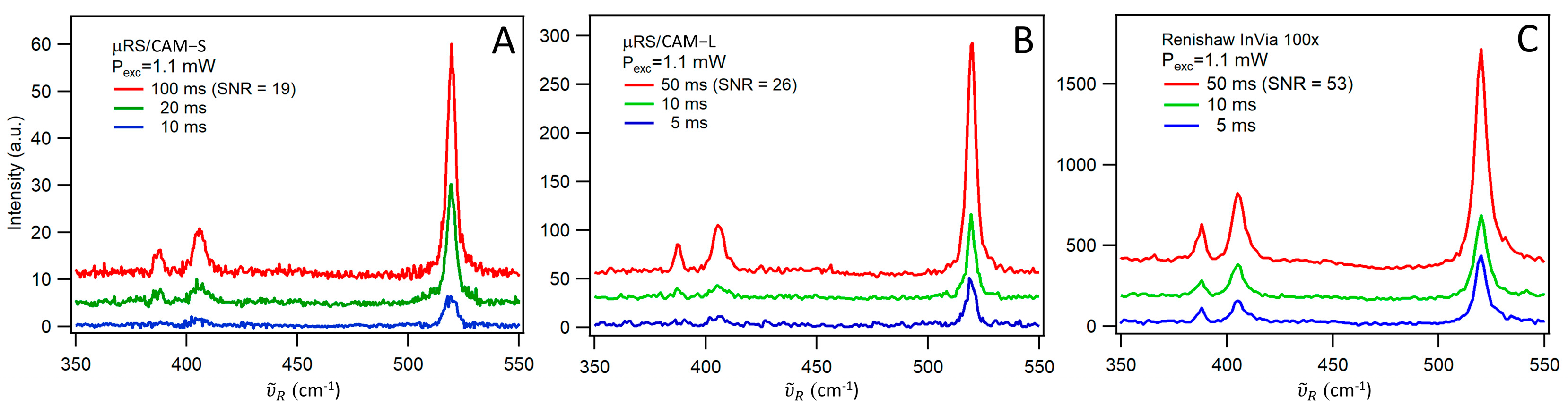
3.3. Signal-to-Noise Comparison with a Commercial High-Resolution Raman Spectrometer

To compare the SNR between µRS with CAM−S, µRS with CAM−L, and the Renishaw InVia confocal Raman microscope with a 100× objective, we ensured that the RSP spot had a comparable diameter and intensity across all systems. This was necessary to maintain consistency in the number of Raman scatterers contributing to the signal.
The RSP spot diameter in the Renishaw InVia with a 100× objective was determined from the device specifications, which state that the best achievable spatial resolution is 300 nm. Assuming the FWHM criterion is used for defining spatial resolution, the RSP spot diameter is taken as 300 nm. To match this in µRS, we adjusted the beam expander so that the FWHM of the RSP spot is also approximately 300 nm (Section S3 in the SM: Equation (S2)). This ensured that all systems had a comparable sampling volume, eliminating the spot size as a variable in the SNR comparison.
To ensure that an equal number of Raman-active molecules contributed to the detected signal, we used an identical excitation power of 1.1 mW for all measurements. Since the excitation volume depends not only on the spot size, but also on the sample thickness, we selected a monolayer of molybdenum disulfide (MoS2) as the SNR calibration sample. The sample is synthesized in-house on the SiO2/Si substrate using chemical vapor deposition (CVD) [28,29] (Section S8 in the SM: Figure S8). MoS2 can exist in both monolayer and multilayer forms, but we ensured that the measured regions corresponded to a monolayer by verifying that the frequency difference between the in-plane E2g1 (388 cm−1) and out-of-plane A1g (406 cm−1) modes was approximately 18–19 cm−1, a known fingerprint for monolayer MoS2 [1].
This methodology ensures that the SNR comparison is fair, with identical excitation conditions, sampling volumes, and Raman-active material densities across all three systems.
Figure 3 presents the measurements obtained with µRS using CAM−S (panel A), µRS using CAM−L (panel B), and Renishaw InVia with a 100× objective (panel C). Apart from the MoS2 peaks, the 520 cm−1 mode of the silicon substrate, assigned to the optical k = 0 phonon [30,31], is also observed.
Exposure times of 5, 10, and 50 ms were used for all setups, except for µRS with CAM−S, where exposure times were doubled. This adjustment was necessary to achieve comparable SNRs across all panels. To quantify the SNR, we selected three Raman spectra that visually exhibited similar SNR levels: 100 ms with CAM−S, 50 ms with CAM−L, and 50 ms with Renishaw InVia 100×. The SNR was calculated by dividing the maximum intensity of the 406 cm−1 peak (signal) by the standard deviation of the dark region between 420 and 450 cm−1 (noise), yielding values ranging from 19 to 53 (see values in parentheses, Figure 3).
These values indicate that the measurements are in the high-photon range, where the SNR follows a square root dependence on the photon irradiance μ p (in photons), as described by the EMVA standard (Equation (22) in ref. [10]):
S N R Q e μ p  
where Q e is the quantum efficiency of the detector. Since μ p is proportional to the exposure time t e x p , the ratio between two SNRs is:
S N R 1 S N R 2 = t e x p 1 t e x p 2  
Thus, if an initial measurement has SNR1 obtained with an exposure time t e x p 1 and a higher SNR2 is desired, the required exposure time t e x p 2 can be calculated as:
t e x p 2 = t e x p 1 S N R 2 S N R 1 2  
In conclusion, from Equation (3), it follows that to achieve the same SNR with µRS using CAM−L as that obtained with Renishaw InVia with a 100× objective (i.e., SNR = 53), the exposure time must be increased by a factor of 4.2, i.e., to 210 ms. For µRS using CAM−S, the required increase in the exposure time is 7.8 times, i.e., to 780 ms. However, in most practical applications, such a high SNR is not necessary, and an exposure time of 50 ms provides a good balance between the signal quality and acquisition speed.

4. Discussion and Conclusions

For the successful deconvolution of the Raman spectrum and the accurate determination of the natural linewidth of any Raman peak, it is necessary to know the spectral resolution function Δ ν ~ S ν ~ R , which describes the spectral resolution across the entire range of Raman shifts dispersed on the detector. The following expression for the spectral resolution function (SRF) is applicable (see ref. [32] and adaptation to our setup in Section S7 in the SM):
ν ~ S ( ν ~ R ) = ( ν ~ L ν ~ R ) 2   W i d f C A M cos θ ,
where ν ~ L is the laser absolute wavenumber, ν ~ R is the Raman shift, W i is the size (FWHM) of the RSP spot image at the detector plane, d is the grating groove spacing, f C A M is the focal length of LCAM, and θ is the diffraction angle (Section S5 in the SM: Equation (S13)).
Using the experimentally determined values of Δ ν ~ S for µRS using CAM−L and µRS using CAM−S, and applying Equation (4), we can calculate W i at various ν ~ R values (Table 1). The results show that W i varies between 10.8 and 14.5 µm. At first glance, this is unexpected, as the magnification factor of the spectrometer is M = f C A M / f S L T = 1, which suggests that the RSP spot image at the slit plane should be directly mapped onto the detector. Since the size of the RSP spot at the slit plane is W S L T = 2.15 µm, we would expect a slightly larger value at the detector, but not the observed variation.
However, the imaging process is not governed solely by ray optics, but is also influenced by diffraction and optical aberrations. Based on their experimental findings, Liu and Berg [32] proposed the following empirical relationship between W S L T and W i :
W i = M W S L T 2 + W l i m i t 2
where W l i m i t represents the smallest achievable FWHM of the slit image. This lower bound is primarily dictated by diffraction and optical aberrations in the spectrometer optics. According to ref. [33], who analyzed the diffraction effects of gratings and circular apertures, W l i m i t can be approximated as:
W l i m i t = A   λ
where A is a constant specific to the optical bench, also referred to as the Diffraction and Aberrations Compensation Factor (DACF). The constant A can be determined by performing a linear regression on Equation (4), using ( λ , W l i m i t ) as the input data points (Table 1). The resulting value of A is the same for both cameras within experimental uncertainty and amounts to A = 21.4. This indicates that the diffraction and aberration effects affecting the spectral resolution are consistent across both detector configurations.
With the obtained value of A , it is now possible to calculate ν ~ S ( ν ~ R ) for the spectral coverage of the µRS. The results are shown in Figure 2B, the blue line, demonstrating how the spectral resolution varies across the spectrum. It can be concluded that the spectral resolution of the µRS ranges from 3 cm−1 to 2.6 cm−1 for Raman shifts between 200 cm−1 and 1400 cm−1.
Carbon tetrachloride (CCl4) is a standard test sample in Raman spectroscopy, frequently used to qualitatively assess the spectral resolution of a Raman spectrometer. Its Raman spectrum features closely spaced peaks around 460 cm−1, which correspond to the symmetric stretch modes of different isotopic variants of CCl4, with a peak-to-peak separation of approximately 3.6 cm−1. In our measurements, we used carbon tetrachloride anhydrous (>99.5%, Sigma-Aldrich, Darmstadt, Germany) without further purification; a 100 µL drop was deposited directly onto the sample holder.
The measured spectra (Figure 4) demonstrate that both Renishaw InVia with a 100× objective and a 20 µm slit, and the µRS with CAM−L begins to show separation between them. However, only with µRS using CAM−S are the peaks fully resolved, allowing the determination of their maximum positions by a simple visual inspection. This improvement is attributed to the better pixel resolution of CAM−S, which provides denser spectral sampling. When dealing with closely spaced peaks, a finer pixel resolution (around 0.4 cm−1 for CAM−S) helps minimize interpolation errors and more accurately captures peak shapes, ultimately enhancing the effective spectral resolution of the spectrometer. Renishaw InVia has the coarsest pixel resolution (around 1.1 cm−1), which is arguably the reason why the peaks are not resolved in its spectrum.
This sample can also serve as a test for the accuracy of Raman shift calibration. We compared the peak positions obtained with µRS using CAM−S with values measured independently with a high-resolution Raman spectrometer (ref. [34], spectral resolution of 1 cm−1). The difference between the measured and reference values ranges from 0.2 to 0.4 cm−1, providing an estimate of the uncertainty of the Raman shift calibration protocol.
In the introduction, we emphasized the importance of a sensitive spectrometer, as having good spectral resolution alone may not be particularly useful if the sensitivity is low. To assess the sensitivity of the µRS, we compared the acquired spectra from three experimental setups under similar conditions, using the same excitation power and analyzing the SNR across different exposure times (Figure 3). The results showed that the SNRs of µRS with CAM−L were half of the SNRs of Renishaw InVia, with µRS with CAM−L requiring 4.2 times longer exposure times than Renishaw InVia with a 100× objective to achieve a similar SNR.
However, µRS with CAM−S has significantly lower sensitivity, requiring an even longer exposure time. Specifically, to match the SNR of Renishaw InVia with a 100× objective, µRS with CAM−S needs almost eight times longer exposure times. Despite this, the example of CCl4 (Figure 4) demonstrates that µRS with CAM−S remains highly effective for certain applications, particularly when resolving closely spaced peaks where its finer pixel resolution provides a significant advantage.
In conclusion, we have designed, constructed, and characterized a micro-Raman spectrometer that is cost-effective and has a footprint at least five times smaller than a typical lab-based Raman spectrometer. Despite its compact design, it delivers a high spectral resolution, ranging from 3 cm−1 to 2.6 cm−1 for Raman shifts between 200 cm−1 and 1400 cm−1. The key factors behind this performance include the use of high-quality photographic objectives, an industrial CMOS camera with a sensitive sensor, and a microscope objective that efficiently couples light from the micro-Raman probe to the spectrometer entrance slit. Although the use of an uncooled CMOS camera imposes some limitations on long integration times—due to an increased dark current and the absence of active cooling—our spectrometer remains well-suited for confocal Raman imaging, where integration times of less than one second per spatial point are typical. However, for applications involving very weak Raman signals (<20 photons/s) that require multi-minute exposure times, the resulting dark noise buildup may reduce SNR, making cooled CCD systems more appropriate in those cases.
By characterizing the system using a monolayer MoS2 sample, we have demonstrated that the sensitivity of our micro-Raman spectrometer, while somewhat lower, remains within a useful range compared to commercial research-grade confocal Raman microscopes, particularly when exposure times are adjusted accordingly.
Despite its simple and cost-effective design, our homebuilt Raman spectrometer achieves a high spectral resolution of 2.6–3 cm−1 and sensitivity within a useful range for advanced research applications. Unlike RGRSs, which are typically expensive and confined to laboratory environments, our µRS is built at a cost one order of magnitude lower, making high-resolution Raman spectroscopy more accessible for diverse research and industrial needs.
This work highlights the potential for individuals with moderate experience in an optical setup assembly to build a compact, high-resolution Raman spectrometer from widely available components. It offers an accessible alternative for researchers, particularly those working in resource-limited environments or requiring portable, in-field Raman measurements.

Supplementary Materials

The following supporting information can be downloaded at: https://www.mdpi.com/article/10.3390/photonics12040389/s1, Table S1: List of main components of the µRS; Table S2: Cost of components of the µRS; Table S3: Cost of commercial high-resolution Raman spectrometers and their technical specifications; Figure S1: Photo of the cost-effective micro-Raman spectrometer (µRS) with a footprint of 60 × 30 cm. For clarity, wires, baffles, and light-shielding enclosures have been removed. Component labels follow the same legends as in Figure 1 of the manuscript; Figure S2: Spectrum of Coherent Compass 315M laser (red crosses) and its gaussian fit (blue line): λ L is the excitation laser wavelength, ν ~ L is the excitation laser wavenumber, Δ ν ~ L is is the excitation laser linewidth (FWHM of the laser spectrum) in wavenumbers; Figure S3: Upper panel: The microscope objective LOBJ focuses the 532.13 nm excitation beam (green), of Gaussian intensity profile and 1/e2 diameter of 2 w 0 e x c   1 / e 2 , onto the sample and creates the RSP spot. The latter has a 2D Gaussian intensity profile with the FWHM diameter of W R S P ; Lower panel: LOBJ and the coupling objective LCPL form a microscope system with 5× magnification that images the RSP spot onto the entrance slit SLT. The FWHM of the RSP spot image at the slit plane (the PSF model is approximated by a Gaussian, see the text) is W S L T ; Figure S4: Incident ray impinging on the grating and diffracted ray for diffraction order m = −1. The incidence angle θ i , the diffraction angle θ ; Figure S5: The collimated beam exiting the slit lens LSLT (Figure 1) has diameter of DSLT while the grating can accept beams of up to ≈14 mm diameter ( l g r cos θ i ) . The latter value limits the light acceptance cone and thus it is limiting factor of the spectrometer’s light gathering power; Figure S6: Raman spectrum of the calcite crystal (red line) and Voigt fits of its Raman peaks (blue line, middle panel and red line, lower panel). The spectrum was measured with µRS with CAM-S (1.85 µm pixel size) as detector, 3 s exposure and 1.6 mW excitation power (middle panel). The residuals of the fits are shown in the upper panel. The peaks were fitted in MultiPeakFit package of Igor Pro; Figure S7: A. The 280 cm−1 and B. the 710 cm−1 Raman peaks of calcite measured with Renishaw InVia with 100× objective and 20 µm slit (black dots), µRS with CAM−L (red dots) and µRS with CAM−S (blue dots). The exposure was 3 s while the excitation power was 1.6 mW. The peaks are normalized; Figure S8: As-grown MoS2 monolayer triangular on SiO2/Si substrate imaged with Renishaw InVia microscope (white light image) at 50X magnification. Purple triangle is the MoS2 monolayer while the bright spot is the excitation laser; Figure S9: Close-up of the MoS2 Raman spectra, focusing on the 406 cm−1 peak. All spectra were acquired using 1.1 mW excitation at 532 nm with the following setups: A. µRS with CAM-S (1.85 µm pixel size) and 100 ms exposure; B. µRS with CAM-L (3.45 µm pixel size) and 50 ms exposure; C. Renishaw InVia confocal Raman microscope with a 100× objective, a 20 µm entrance slit and 50 ms exposure. References [35,36,37,38] are cited and used in the Supplementary Materials.

Author Contributions

Conceptualization, G.Z. and D.Č.; Funding acquisition, M.R.; Investigation, G.Z., D.Č. and A.S.; Methodology, G.Z. and D.Č.; Project administration, M.R.; Supervision, M.R.; Visualization, G.Z. and M.R.; Writing—original draft, G.Z.; Writing—review and editing, G.Z., D.Č. and M.R. All authors have read and agreed to the published version of the manuscript.

Funding

We acknowledge the support of the project Compact Raman device with advanced features, NPOO.C3.2.R3-I1.02.0005, financed by the European Union through the National Recovery and Resilience Plan 2021–2026. This work was also supported by the project the Center for Advanced Laser Techniques (CALT), co-funded by the European Union through the European Regional Development Fund under the Competitiveness and Cohesion Operational Program (grant no. KK.01.1.1.05.0001).

Institutional Review Board Statement

Not applicable.

Informed Consent Statement

Not applicable.

Data Availability Statement

The data that support the findings of this study are available from the corresponding author upon reasonable request.

Conflicts of Interest

The authors declare no conflicts of interest.

Abbreviations

The following abbreviations are used in this manuscript:
µRSMicro-Raman Spectrometer
CMOSComplementary Metal-Oxide Semiconductor
RGRSResearch-Grade Raman Spectrometers
FRS Fiber Raman Spectrometer
DNDark Noise
QeQuantum Efficiency
OBTOptical Bench Throughput
NIRNear Infrared
VISVisible
iCMOSIndustrial-Grade CMOS Camera
CCDCharge-Coupled Device
sCMOSScientific-Grade CMOS
EMCCDElectron-Multiplying CCD
sCCDScientific-Grade CCD
CAM-LiCMOS with 3.45 µm pixel size
CAM-SiCMOS with 1.85 µm pixel size
µRS/CAM−LMicro-Raman Spectrometer with CAM−L camera
µRS/CAM−SMicro-Raman Spectrometer with CAM−S camera
CAMIndustrial-grade CMOS Camera
LCAMCamera Lens
LSLTSlit Lens
GDiffraction Grating with 2400 lines/mm
SLT5 µm wide slit
LNarrow Linewidth Laser at 532.13 nm
BEBeam Expander
MFolding Mirror
FRRaman Edge Filter at 532 nm
LOBJCollection Objective
LCPLCoupling Objective
SLMSingle Longitudinal Mode
DPSSDiode-Pumped Solid-State
RSPRaman-Scattered Photons
ULFUltra-Low Frequency
FWHMFull with at half maximum
PSFPoint Spread Function
NANumerical Aperture
SNRSignal-to-noise
ASTMAmerican Society for Testing Materials

References

  1. Lee, C.; Yan, H.; Brus, L.E.; Heinz, T.F.; Hone, J.; Ryu, S. Anomalous Lattice Vibrations of Single- and Few-Layer MoS2. ACS Nano 2010, 4, 2695–2700. [Google Scholar] [CrossRef] [PubMed]
  2. Chen, X.; Stoneburner, K.; Ladika, M.; Kuo, T.-C.; Kalantar, T.H. High-Throughput Raman Spectroscopy Screening of Excipients for the Stabilization of Amorphous Drugs. Appl. Spectrosc. 2015, 69, 1271–1280. [Google Scholar] [CrossRef] [PubMed]
  3. Nielsen, A.S.; Batchelder, D.N.; Pyrz, R. Estimation of Crystallinity of Isotactic Polypropylene Using Raman Spectroscopy. Polymer 2002, 43, 2671–2676. [Google Scholar] [CrossRef]
  4. Threlfall, T.L. Analysis of Organic Polymorphs. A Review. Analyst 1995, 120, 2435–2460. [Google Scholar] [CrossRef]
  5. Tudor, A.M.; Davies, M.C.; Melia, C.D.; Lee, D.C.; Mitchell, R.C.; Hendra, P.J.; Church, S.J. The Applications of Near-Infrared Fourier Transform Raman Spectroscopy to the Analysis of Polymorphic Forms of Cimetidine. Spectrochim. Acta A 1991, 47, 1389–1393. [Google Scholar] [CrossRef]
  6. Wermelinger, T.; Spolenak, R. Stress Analysis by Means of Raman Microscopy. In Confocal Raman Microscopy; Toporski, J., Dieing, T., Hollricher, O., Eds.; Springer International Publishing: Cham, Switzerland, 2018; pp. 509–529. [Google Scholar] [CrossRef]
  7. Ikushima, Y.; Hatakeda, K.; Saito, N.; Arai, M. An in Situ Raman Spectroscopy Study of Subcritical and Supercritical Water: The Peculiarity of Hydrogen Bonding near the Critical Point. J. Chem. Phys. 1998, 108, 5855–5860. [Google Scholar] [CrossRef]
  8. Oladepo, S.A.; Xiong, K.; Hong, Z.; Asher, S.A. Elucidating Peptide and Protein Structure and Dynamics: UV Resonance Raman Spectroscopy. J. Phys. Chem. Lett. 2011, 2, 334–344. [Google Scholar] [CrossRef]
  9. Polli, D.; Kumar, V.; Valensise, C.M.; Marangoni, M.; Cerullo, G. Broadband Coherent Raman Scattering Microscopy. Laser Photonics Rev. 2018, 12, 1800020. [Google Scholar] [CrossRef]
  10. European Machine Vision Association. EMVA Standard 1288—Standard for Characterization of Image Sensors and Cameras. Available online: https://www.emva.org/standards-technology/emva-1288/emva-standard-1288-downloads-2/ (accessed on 5 April 2025).
  11. Dieing, T.; Hollricher, O.; Toporski, J. Confocal Raman Microscopy, 2nd ed; Springer: Cham, Switzerland, 2018. [Google Scholar] [CrossRef]
  12. Dieing, T.; Hollricher, O. High-Resolution, High-Speed Confocal Raman Imaging. Vib. Spectrosc. 2008, 48, 22–27. [Google Scholar] [CrossRef]
  13. Fossum, E.R. The Invention of CMOS Image Sensors: A Camera in Every Pocket. In Proceedings of the 2020 Pan Pacific Microelectronics Symposium (Pan Pacific), Big Island, HI, USA, 10–13 February 2020. [Google Scholar] [CrossRef]
  14. FLIR. Camera Sensor Review. 2023. Available online: https://www.flir.com/landing/iis/machine-vision-camera-sensor-review/ (accessed on 5 April 2025).
  15. Ma, H.; Fu, R.; Xu, J.; Liu, Y. A Simple and Cost-Effective Setup for Super-Resolution Localization Microscopy. Sci. Rep. 2017, 7, 1–9. [Google Scholar] [CrossRef]
  16. Diekmann, R.; Till, K.; Müller, M.; Simonis, M.; Schüttpelz, M.; Huser, T. Characterization of an Industry-Grade CMOS Camera Well Suited for Single Molecule Localization Microscopy—High Performance Super-Resolution at Low Cost. Sci. Rep. 2017, 7, 14425. [Google Scholar] [CrossRef] [PubMed]
  17. Hasinoff, S.W.; Durand, F.; Freeman, W.T. Noise-Optimal Capture for High Dynamic Range Photography. In Proceedings of the 2010 IEEE Computer Society Conference on Computer Vision and Pattern Recognition, San Francisco, CA, USA, 13–18 June 2010; pp. 553–560. [Google Scholar] [CrossRef]
  18. Lin, M.L.; Ran, F.R.; Qiao, X.F.; Wu, J.B.; Shi, W.; Zhang, Z.H.; Xu, X.Z.; Liu, K.H.; Li, H.; Tan, P.H. Ultralow-Frequency Raman System down to 10 cm−1 with Longpass Edge Filters and Its Application to the Interface Coupling in t(2+2)LGs. Rev. Sci. Instrum. 2016, 87, 053122. [Google Scholar] [CrossRef] [PubMed]
  19. Pawley, J.B. Handbook of Biological Confocal Microscopy, 3rd ed; Springer: New York, NY, USA, 2006. [Google Scholar] [CrossRef]
  20. Gu, M. Advanced Optical Imaging Theory; Springer: Berlin/Heidelberg, Germany, 2013. [Google Scholar] [CrossRef]
  21. Zhang, B.; Zerubia, J.; Olivo-Marin, J.-C. Gaussian Approximations of Fluorescence Microscope Point-spread Function Models. Appl. Opt. 2007, 46, 1819–1829. [Google Scholar] [CrossRef] [PubMed]
  22. Freebody, N.A.; Vaughan, A.S.; MacDonald, A.M. On Optical Depth Profiling Using Confocal Raman Spectroscopy. Anal. Bioanal. Chem. 2010, 396, 2813–2823. [Google Scholar] [CrossRef]
  23. Macdonald, A.M.; Vaughan, A.S. Numerical Simulations of Confocal Raman Spectroscopic Depth Profiles of Materials: A Photon Scattering Approach. J. Raman Spectrosc. 2007, 38, 584–592. [Google Scholar] [CrossRef]
  24. Zgrablić, G.; Senkić, A.; Vidović, N.; Užarević, K.; Čapeta, D.; Brekalo, I.; Rakić, M. Building a Cost-Effective Mechanochemical Raman System: Improved Spectral and Time Resolution for in Situ Reaction and Rheology Monitoring. Phys. Chem. Chem. Phys. 2025, 27, 5909–5920. [Google Scholar] [CrossRef]
  25. Ntziouni, A.; Thomson, J.; Xiarchos, I.; Li, X.; Bañares, M.A.; Charitidis, C.; Portela, R.; Lozano Diz, E. Review of Existing Standards, Guides, and Practices for Raman Spectroscopy. Appl. Spectrosc. 2022, 76, 747–772. [Google Scholar] [CrossRef]
  26. ASTM E2529-06; Standard Guide for Testing the Resolution of a Raman Spectrometer. ASTM International: West Conshohocken, PA, USA, 2014. [CrossRef]
  27. Bowie, B.T.; Griffiths, P.R. Determination of the Resolution of a Multichannel Raman Spectrometer Using Fourier Transform Raman Spectra. Appl. Spectrosc. 2003, 57, 190–196. [Google Scholar] [CrossRef]
  28. Delač Marion, I.; Čapeta, D.; Pielić, B.; Faraguna, F.; Gallardo, A.; Pou, P.; Biel, B.; Vujičić, N.; Kralj, M. Atomic-Scale Defects and Electronic Properties of a Transferred Synthesized MoS2 Monolayer. Nanotechnology 2018, 29, 305703. [Google Scholar] [CrossRef]
  29. Lee, Y.-H.; Zhang, X.-Q.; Zhang, W.; Chang, M.-T.; Lin, C.-T.; Chang, K.-D.; Yu, Y.-C.; Wang, J.T.-W.; Chang, C.-S.; Li, L.-J.; et al. Synthesis of Large-Area MoS2 Atomic Layers with Chemical Vapor Deposition. Adv. Mater. 2012, 24, 2320–2325. [Google Scholar] [CrossRef]
  30. Temple, P.A.; Hathaway, C.E. Multiphonon Raman Spectrum of Silicon. Phys. Rev. B 1973, 7, 3685–3697. [Google Scholar] [CrossRef]
  31. Menendez, J.; Cardona, M. Temperature Dependence of the First-Order Raman Scattering by Phonons in Si, Ge, and a-Sn: Anharmonic Effects. Phys. Rev. B 1984, 29, 2051–2059. [Google Scholar] [CrossRef]
  32. Liu, C.; Berg, R.W. Determining the Spectral Resolution of a Charge-Coupled Device (CCD) Raman Instrument. Appl. Spectrosc. 2012, 66, 1034–1043. [Google Scholar] [CrossRef]
  33. Hecht, E. Optics; Addison-Wesley: San Francisco, CA, USA, 2002. [Google Scholar]
  34. Gadomski, W.; Ratajska-Gadomska, B.; Polok, K. Fine Structures in Raman Spectra of Tetrahedral Tetrachloride Molecules in Femtosecond Coherent Spectroscopy. J. Chem. Phys. 2019, 150, 244505. [Google Scholar] [CrossRef]
  35. Teich, M.C.; Saleh, B.E.A. Fundamentals of Photonics; Wiley-Interscience: Hoboken, NJ, USA, 2007. [Google Scholar]
  36. Hauer, P.; Grand, J.; Djorovic, A.; Willmott, G.R.; Le Ru, E.C. Spot Size Engineering in Microscope-Based Laser Spectroscopy. J. Phys. Chem. C 2016, 120, 21104–21113. [Google Scholar] [CrossRef]
  37. Abbe, E. On the Estimation of Aperture in the Microscope. J. Royal Microsc. Soc. 1881, 1, 388–423. [Google Scholar] [CrossRef]
  38. Hermans, R.I.; Seddon, J.; Shams, H.; Ponnampalam, L.; Seeds, A.J.; Aeppli, G. Ultra-high-resolution software-defined photonic terahertz spectroscopy. Optica 2020, 7, 1445. [Google Scholar] [CrossRef]
Figure 1. The scheme of the cost-effective micro-Raman spectrometer (µRS). The high-resolution and high-sensitivity lens-based spectrometer (left box) consists of the following: CAM is an industrial-grade CMOS camera without cooling; LCAM is the camera lens and LSLT is the slit lens—both are photographic objectives with a focal length of 50 mm; G is a diffraction grating with 2400 lines/mm; and SLT is a 5 µm wide slit. The micro-Raman probe (right box) consists of the following: L is a narrow linewidth laser at 532.13 nm; BE is the beam expander made of two plano-convex singlet lenses; M is the folding mirror; FR is a Raman edge filter at 532 nm; LOBJ is the collection objective and LCPL is the coupling objective—both are infinity corrected and together form a 5X microscope; and S is the sample on sample holder which is mounted on a XYZ translation stage. The RSP spot size W R S P , the RSP spot size at the slit plane W S L T , and the RSP spot size at the detector plane W i are denoted next to their respective focal planes in the setup. The green beam denotes the excitation laser path, while the orange beam represents the path of Raman-scattered photons.
Photonics 12 00389 g001
Figure 2. (A). Raman spectrum of calcite crystal measured with µRS with CAM−S as detector using exposure of 3 s and excitation power of 1.6 mW. (B). Experimentally evaluated spectral resolution Δ ν ~ S by using three calcite peaks that have been measured with Renishaw InVia with 100× objective (black dots), µRS with CAM−L (red dots), and µRS with CAM−S (blue dots). The exposure and excitation power were as in A. The spectral resolution function of the µRS (both cameras) is shown as blue line. (C). The 1085 cm−1 peak of calcite measured with Renishaw InVia and 100× objective (black curve), with µRS with CAM−L (red curve), and with µRS with CAM−S (blue curve). The peaks are normalized.
Photonics 12 00389 g002
Figure 3. Monolayer of MoS2 deposited on the SiO2/Si substrate used as the SNR calibration sample. Raman spectra of the sample obtained with: (A). µRS with CAM−S (1.85 µm pixel size); (B). µRS with CAM−L (3.45 µm pixel size); and (C). Renishaw InVia confocal Raman microscope with a 100× objective. In all experiments, a 1.1 mW excitation at 532 nm was used. The camera exposure times are color-coded, and the two longest exposure spectra have been shifted for clarity. In each panel, for the longest exposure spectra, the SNR value was given in parenthesis.
Photonics 12 00389 g003
Figure 4. Comparison of Raman spectra of carbon tetrachloride (CCl4) measured with Renishaw InVia with a 100× objective, a 20 μm slit and an exposure of 2.5 s (black line), µRS with CAM−L and an exposure of 2.5 s (red line), and µRS with CAM−S and an exposure of 10 s (blue line). Dots indicate the pixel positions. The table (inset) presents the following values: ν ~ R E F as the central position of the Raman peak from ref. [34] and ν ~ as the difference between the central position of the Raman peak measured with µRS and the reference value.
Photonics 12 00389 g004
Table 1. Parameters of the spectrometer and of the calcite Raman peaks from Figure 2: central position of the peak ν ~ R ; natural linewidth Γ ; the FWHM of the peak ν ~ M ; experimental spectral resolution ν ~ S ; the FWHM of the RSP spot image at the detector W i ; the smallest possible FWHM of the slit image W l i m i t ; and wavelength λ .
Detector ν ~ R
[cm−1]
Γ
[cm−1]
ν ~ M
[cm−1]
ν ~ S
[cm−1]
W i
[µm]
W l i m i t
[µm]
λ
[µm]
CAM−L280910.33.614.514.30.5402
71023.92.711.611.40.5530
108513.02.410.810.60.5648
CAM−S280910.13.413.713.50.5402
71023.82.611.211.00.5530
108513.12.511.311.10.5648
Disclaimer/Publisher’s Note: The statements, opinions and data contained in all publications are solely those of the individual author(s) and contributor(s) and not of MDPI and/or the editor(s). MDPI and/or the editor(s) disclaim responsibility for any injury to people or property resulting from any ideas, methods, instructions or products referred to in the content.

