1. Introduction
With the exponential growth of data interaction, edge computing, and high-definition live streaming, optical networks have attracted considerable attention over the past decade due to their favorable characteristics, including high speed, large capacity, and low power consumption. Meanwhile, the rapid advancement of emerging technologies has rendered optical network security increasingly vulnerable to sophisticated cyberattacks and malicious intrusions [
1]. Optical networks can be affected by different threats depending on their coverage and type [
2]. To enhance the security of optical networks, several approaches leveraging optical signal processing have been proposed, such as optical code-division multiple access (OCDMA) [
3], all-optical encryption [
4], optical steganography [
5], and optoelectronic firewalls [
6]. As an effective access control mechanism, an optoelectronic firewall leverages all-optical pattern recognition to perform direct detection and analysis of data transmitted through the optical network at the optical layer. Subsequently, it activates the appropriate protection scheme according to the predefined security protocols. Compared with conventional firewalls, it is efficient in filtering malicious traffic within a high-speed data stream since optical-electrical-optical conversion can be avoided. Given the increasing data rate and growing sophistication of malicious network attacks, it is essential to extend the functionality of the firewall to the optical layer and thus implement effective access control directly at the optical layer.
The widely investigated optoelectronic firewall originated from the Wirespeed Security Domains using Optical Monitoring (WISDOM) project led by the European Union. It was specifically designed to address inherent vulnerabilities and mitigate cyber threats within packet-switched network architectures. Experimental results show that it can recognize on-off keying (OOK) targets with lengths spanning from 8 to 256 bits with a data rate of 42.6 Gbps [
7].
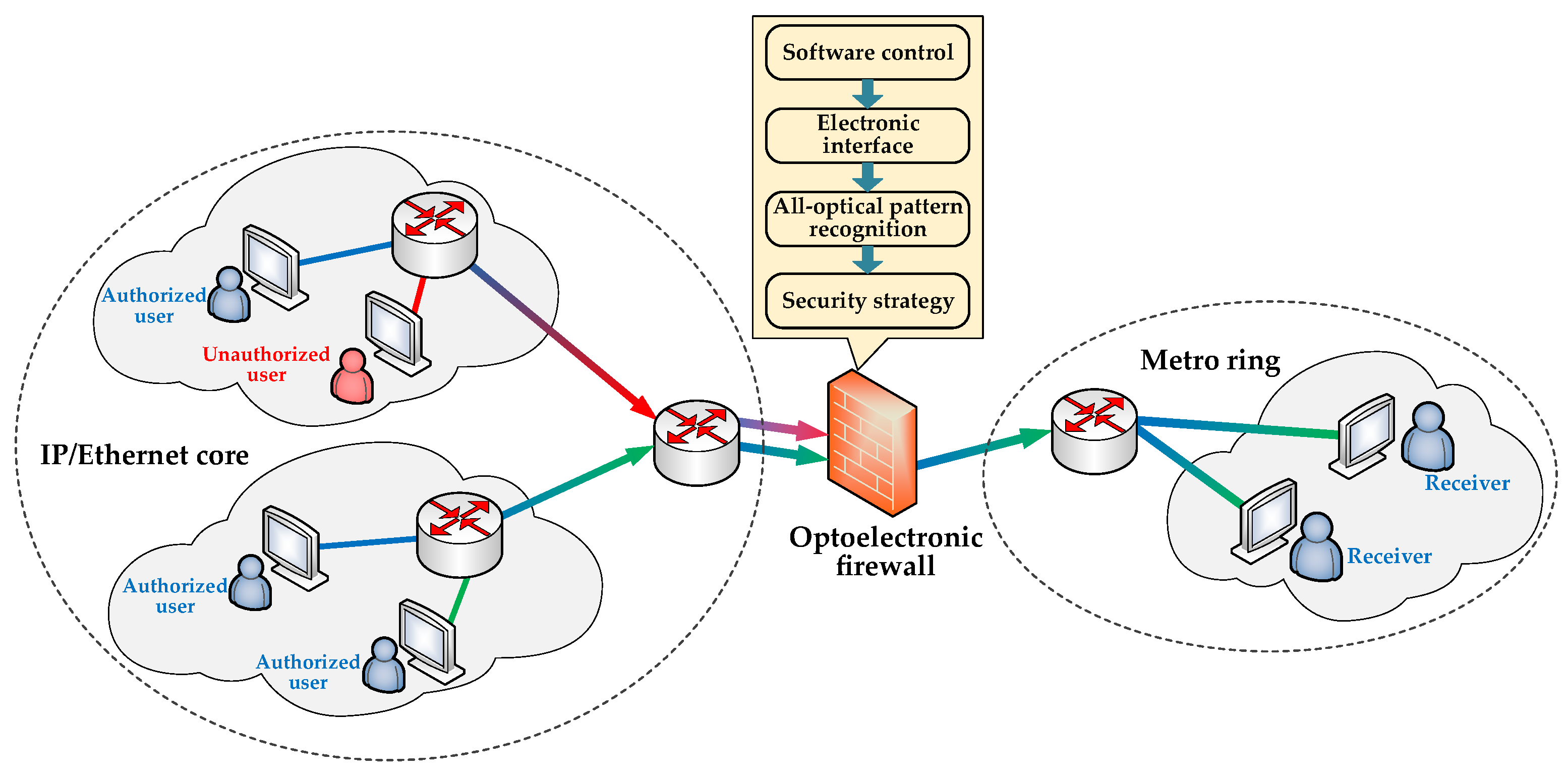
Figure 1 shows the principle and deployment of an optoelectronic firewall. The optoelectronic firewall is located at the edge of optical networks, which provides primary optical information filtering at the router front end. It enables high-speed security monitoring of optical signals directly at the optical layer. Typically, an optoelectronic firewall can be deployed between the IP/Ethernet core and the metro ring, which belongs to the backbone network. When the input data is transmitted through a router to the optoelectronic firewall, the all-optical pattern recognition system inside the optoelectronic firewall conducts simple but high-speed comparison and inspection with the target sequence provided by the electronic interface. The all-optical pattern recognition system developed in WISDOM primarily comprises an XNOR gate, an AND gate, and a regenerator, all of which are implemented using semiconductor optical amplifier-based Mach-Zehnder interferometers (SOA-MZIs). Meanwhile, the electronic interface can be reconfigured by software control to obtain different target sequences. Finally, the security strategy module implements optical prefiltering based on the output results generated by the all-optical pattern recognition system.
To reduce recognition time, an all-optical binary recognition system with parallel structure was proposed for short sequence detection in [
8]. It can recognize 8-bit OOK signals operating at 40 Gbps. However, the size of the system exhibits a linear correlation with the length of the target. Restricted by the carrier recovery time of SOA, a binary sequence matching system based on highly nonlinear fiber (HNLF) was proposed in [
9]. Owing to the short response time of HNLF, it can recognize 8-bit targets in 64-bit OOK data at 160 Gbps. Meanwhile, phase modulation formats like binary phase shift keying (BPSK) and quadrature phase shift keying (QPSK) are extensively utilized in commercial optical communication devices because of their benefits, including extended transmission distances and robust resistance to noise [
10]. An all-optical flexible matching system for OOK, BPSK, and polarization shift keying (PolSK) signals was developed in [
11]. It can avoid phase-locking through all-optical format conversion and parallel structure. For higher-order phase-modulated signals, two all-optical pattern recognition systems based on format conversion [
12] and parallel structure [
13] were proposed to recognize QPSK symbols. To improve flexibility and scalability, a reconfigurable all-optical pattern-matching system for phase-modulated signals based on phase-sensitive amplification was proposed in [
14]. Recently, a reconfigurable all-optical pattern recognition system was proposed for PSK and quadrature amplitude modulation (QAM) signals with two implementation architectures [
15].
Although many works have studied the recognition of phase-modulated signals, there are still three issues that need to be addressed when an optoelectronic firewall is deployed in optical networks. First, frequency synchronization brought on by phase-locking leads to a complex system. Although the systems in [
11,
13] achieve a phase-locking-free architecture, the parallel structure makes the system complex and bulky when recognizing long target sequences. Other works all require additional frequency synchronization or phase-locking devices to maintain a stable frequency or phase relationship between the input data and the target, which also increases the complexity of the whole system. Second, a single pattern recognition system cannot recognize more than one target each time. As network attacks become sophisticated and insidious, it is necessary to recognize more than one target with arbitrary length without cost and complexity increasing. Third, the previous systems cannot support the recognition of input signals with tunable frequency. They can only achieve pattern recognition of input signals with a specific frequency.
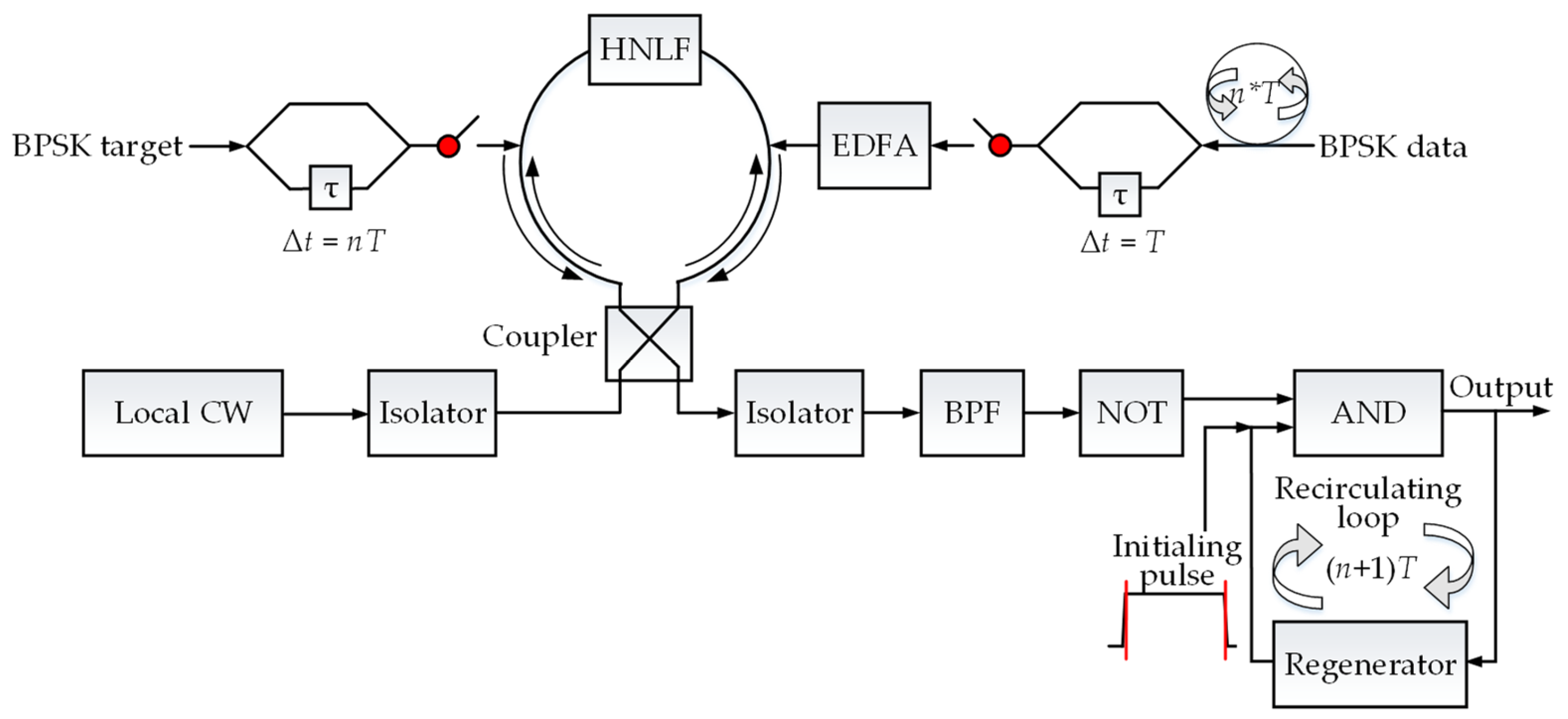
In this paper, we propose a tunable all-optical pattern recognition system based on a nonlinear optical loop mirror (NOLM). The system mainly consists of two delay interferometers (DLs), the NOLM, a NOT gate, and the recirculating loop, including an AND gate and a regenerator. The significant contributions of our study span four aspects: (1) our proposed system is phase-locking free. Benefiting from the signal reloading and the symmetric design of NOLM, the generation and maintenance of a stable phase relationship between the input data and target are inherently guaranteed, thereby eliminating the need for additional phase-locking or signal carrier extraction; (2) the system can recognize two bit-flip BPSK targets at the same time. Due to differential encoding, the phase difference between adjacent bits of the BPSK signal is mapped into a two-level power-modulated signal through DI. Then, two bit-flip BPSK targets are reloaded as the same output signal. By recognizing the reloaded signal, the recognition results for the original two bit-flip BPSK targets can be obtained; (3) the system can process the input signal with tunable frequency. By adjusting the gain of EDFA and controlling the signal power entering NOLM, the phase shift resulting from the XPM effect for the input signal with tunable frequency is ensured to be either π or 0. Thus, our proposed system can process the input signal with different frequencies; (4) the system can be extended to support higher-order modulation formats. By substituting the DI with an all-optical format conversion that transforms QPSK signals into four-level pulse amplitude modulation (PAM4) signals, the proposed system can be extended to support the recognition of QPSK targets, which enhances its compatibility and configurability. Detailed structure design and operation principles are illustrated. To evaluate the feasibility of the proposed system, simulations are conducted through VPItransmissionMaker 8.5, a photonics design and simulation software developed by VPIphotonics, with its headquarters located in Berlin, Germany. Numerical simulations demonstrate that the proposed system can accurately recognize and determine the position of bit-flip BPSK targets in the input data with a data rate of 100 Gbps and tunable frequency.
The rest of this paper is organized as follows.
Section 2 details the operational principles of the proposed system.
Section 3 describes the simulation setup and system parameters. Simulation results are presented and discussed in
Section 4.
Section 5 concludes this paper.
2. Principle of Operation
The schematic diagram of the proposed all-optical pattern recognition system is shown in
Figure 2. Initially, the input BPSK data with a length of
n bits is repeated
m times via the storage loop with a duration of
nT. Here,
m represents the number of bits in the BPSK target, and
T represents the bit period of the input data. The phase information is mapped into a power-modulated signal, which is characterized by an alternative mark inversion (AMI) pattern through the 1-bit DI. Assuming the two optional phases of the BPSK signal are 0 and π, the former is encoded as 0, and the latter is encoded as 1. Then, the output power of the AMI pattern,
PAMI = 0, corresponds to the consecutive bit sequence (10, 01), and
PAMI ≠ 0 corresponds to the consecutive bit sequence (00, 11). If the electrical field of the input BPSK signal is denoted as
Ein, the electrical fields of the upper arm
Eupper1-R and lower arm
Elower1-R after entering the first Y branch in the right DI can be expressed as
Equation (1) describes the electric field distribution of the input BPSK signal
Ein after passing through the first Y branch of the right DI. The lower arm signal acquires an additional
j phase factor due to the DI, while the upper arm signal remains unchanged. The electrical fields of the upper arm
Eupper2-R and lower arm
Elower2-R after entering the second Y branch in the right DI can be expressed as Equation (2), where Δ
φin is the adjacent bit phase difference of the input BPSK signal.
Equation (2) further illustrates the electric field distribution after passing through the second Y branch. Notably, signals in both the upper and lower arms are influenced by the phase difference Δ
φin between adjacent bits, causing rotation in the IQ plane. Equations (1) and (2) demonstrate how the phase information of the input BPSK signal is converted into amplitude information via the DI, which is the first step in achieving phase-modulated signal to amplitude signal conversion. Here, we select the lower arm as the output; the output power of the right DI
PAMI-R can be obtained as Equation (3), where
Pin = |
Ein|
2 denotes the power of the input signal.
Equation (3) calculates the output power
PAMI-R at the right DI, which depends on the input signal power
Pin and the phase difference Δ
φin. For BPSK signals with phase states 0 or π, cos(2Δ
φin) can only be 1 or −1, resulting in two distinct power levels. This corresponds to the generation of alternate mark inversion (AMI) or duobinary signals. Equation (3) explains how the DI maps the phase information of BPSK signals into two power levels, enabling subsequent signal processing.
Next, the following optical switch is initially open and then closed at the beginning of the second loop. The output of the right DI enters the erbium-doped fiber amplifier (EDFA) to amplify the power to
PXPM, which is required in the subsequent cross-phase modulation (XPM) process. Similarly, the BPSK target is periodically generated with a duration of
nT. Then, the phase information of the target is mapped into a power-modulated signal through the
n-bit DI. Here, we assume that the electrical field of the BPSK target is denoted as
Et, then the electrical fields of the upper arm
Eupper1-L and lower arm
Elower1-L after entering the first Y branch in the left DI can be expressed as
The electrical fields of the upper arm
Eupper2-L and lower arm
Elower2-L after entering the second Y branch in the left DI can be expressed as Equation (5), where Δφ
t is the adjacent bit phase difference of the BPSK target.
Again, we select the lower arm as the output, then the output power of the left DI
PAMI-L can be obtained as Equation (6), where
Pt = |
Et|
2 denotes the power of the target. Equations (4)–(6) describe the processing of the BPSK target
Et by the left DI. Their physical meaning and function align with those of the right DI, but they apply to a different signal. The setting of the following optical switch is the same as that of the right one.
Meanwhile, the continuous wave (CW) with a center frequency of
λCW generated by the local laser is separated into two branches after traversing a unidirectional isolator and a 50:50 coupler. These two branches are injected into the NOLM using bidirectional HNLF as a nonlinear medium, and transmitted clockwise and counterclockwise, respectively, in the NOLM. If the electrical field of the local CW is denoted as
ECW, the electrical fields of the clockwise carrier
EC and counterclockwise carrier
ECC can be expressed as
Equation (7) describes the electric field distribution of the local CW
ECW divided into clockwise
EC and counterclockwise
ECC components. Then, the XPM effect occurs between the clockwise carrier, which serves as the probe, and the output of the left DI, which serves as the pump, inside the bidirectional HNLF. Similarly, the XPM effect occurs between the counterclockwise carrier and the output of the right DI at the same time. As the power of two pumps carries the phase information of the target and the input data, they are reloaded on the clockwise and counterclockwise carriers, respectively. Specifically, the phase shift
φXPM induced by XPM is characterized as Equation (8), where
γ and
Leff represent the nonlinear coefficient and the effective length of the bidirectional HNLF, respectively.
PXPM is the pump power required to make 2
γLeffPXPM = π.
Equation (8) defines the phase shift
φXPM induced by XPM, which is proportional to the fiber’s nonlinear coefficient
γ, effective interaction length
Leff, and pump power
PXPM. By controlling the pump power and fiber parameters, we can ensure that the probe signal is properly modulated, thereby achieving signal reloading. Here, we adjust
PAMI-R and
PAMI-L by setting the proper gain of the EDFA and controlling the output power of the target, such that
PAMI-R and
PAMI-L are either 0 or
PXPM for different consecutive bit sequences. After interacting inside the bidirectional HNLF,
PAMI-R = 0 is reloaded as
φR-in = 0, where
φR-in denotes the phase of the reloaded BPSK signal, while
PAMI-R ≠ 0 is reloaded as
φR-in = π. Meanwhile,
PAMI-L = 0 is reloaded as
φR-t = 0, where
φR-t denotes the phase of the reloaded BPSK target, while
PAMI-L ≠ 0 is reloaded as
φR-t = π. Here, the phase shift brought by the self-phase modulation (SPM) effect is ignored due to the low power of the probe. In this way, the phase-amplitude-phase conversion is completed. Two reloaded BPSK signals are coherently interfered at the output of the 50:50 coupler. Assuming the electrical field of the forward output which is close to the right isolator is denoted as
Efw, and the electrical field of the backward output which is close to the left isolator is denoted as
Ebw, the above process can be expressed as Equation (9), where
EAMI-L and
EAMI-R are the electrical fields of the output of the left DI and right DI, respectively.
Equation (9) calculates the forward output electric field
Efw near the right isolator after passing through the NOLM. It incorporates interference between clockwise/counterclockwise carriers and AMI signals, as well as XPM-induced phase shifts. Next, the forward output
Efw is filtered through the band pass filter (BPF) with a center frequency of
λCW. The electrical field of the output of the BPF,
EBPF, is shown in Equation (10).
Equation (10) represents the filtered output
EBPF after the BPF, which isolates the wavelength of the local CW
λCW. Equations (7)–(10) model the signal transmission, interference in NOLM, and filtering processes, which are critical for achieving phase-locking-free bit-recognition.
It can be noted that the reloaded BPSK signal has π phase deflection because it goes through the 50:50 coupler twice. When the input signal is in phase with the target, there will be no pulse indicating logic “0” generated at the output of the BPF. Conversely, when the input signal is out of phase with the target, a pulse indicating logic “1” will be generated.
Figure 3 shows the schematic diagram of the constellation transformation and corresponding bit sequence mapping during bit-recognition. The primary phases of signal processing include DI, XPM, and coupling. The original BPSK signal is first converted into the AMI pattern after the DI. Then, the AMI pattern is reloaded to the phase-modulated signal leveraging the XPM effect. The two reloaded signals are coupled to obtain the bit-recognition result. According to the bit-recognition result, when the adjacent bit phase difference of the input BPSK signal and the target are the same, which means both are π or 0, the output of the coupler is logic “0”. Otherwise, when the adjacent bit phase difference of the input BPSK signal and the target are different, the output of the coupler is logic “1”. Next, the bit-recognition result passes through an EDFA and a NOT gate. If the input signal is in phase with the target, there is a pulse indicating logic “1” generated after the NOT gate; otherwise, no pulse indicating logic “0” is generated after the NOT gate. Finally, a recirculating loop integrating an AND gate and a regenerator with (
n + 1) bits delay is connected to recognize the target with variable length. This is the same as that in [
7], so we will not go into detail here.
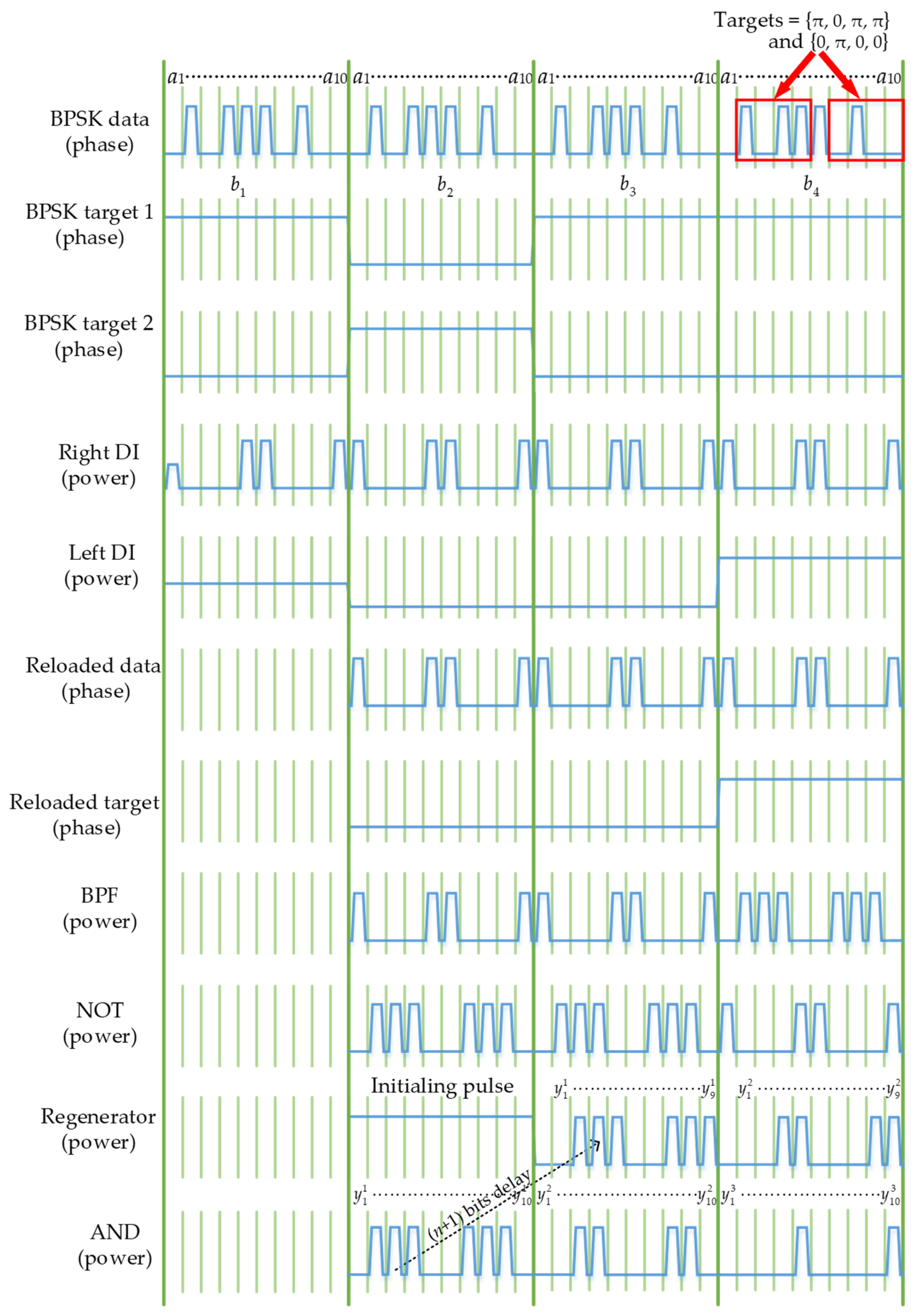
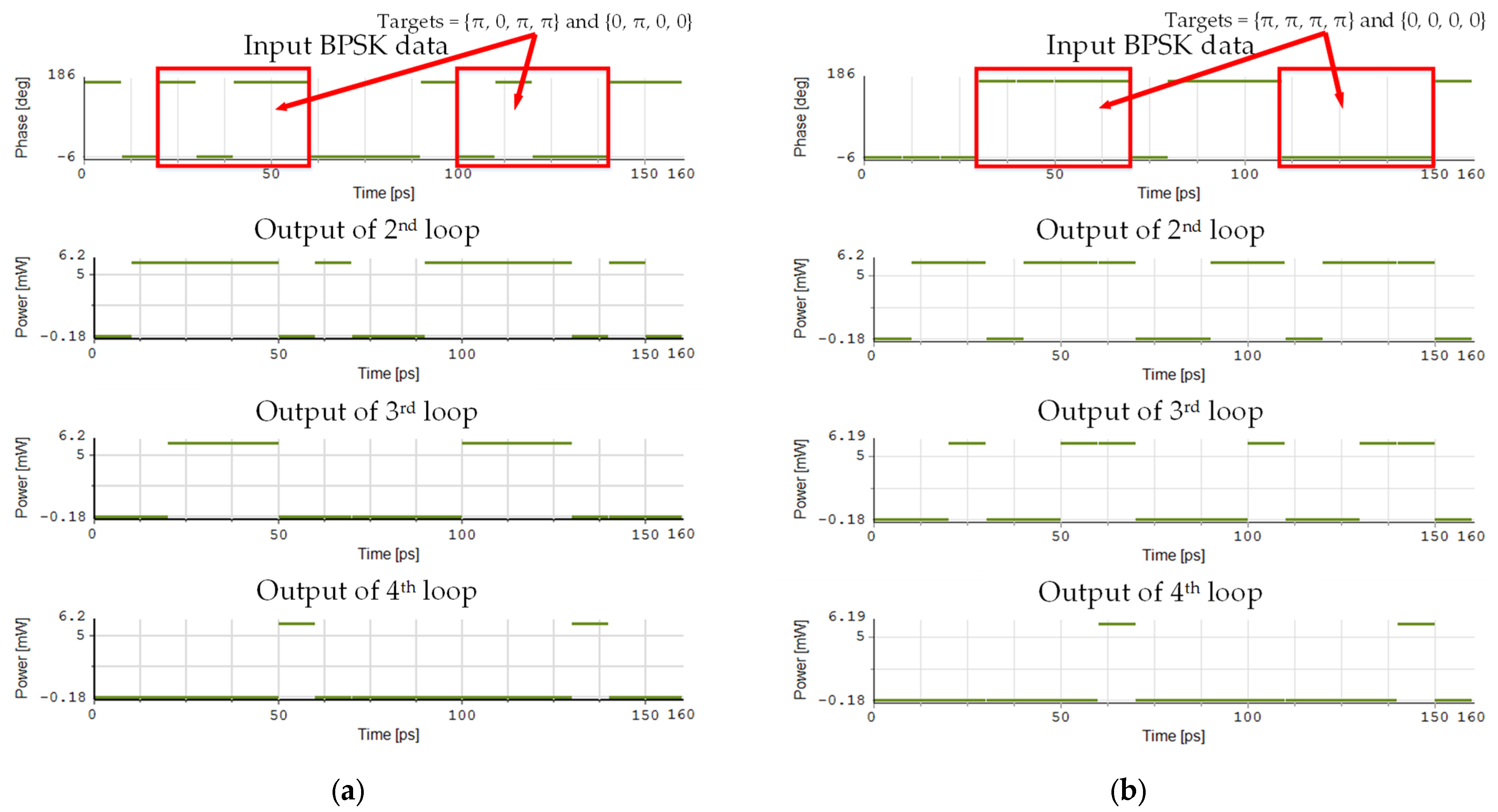
The procedure of searching targets {π, 0, π, π} and {0, π, 0, 0} in the input data {0, π, 0, π, π, π, 0, π, 0, 0} is shown in
Figure 4. Here, we assume that the time for signals to pass through optical fibers and other components is ignored. In the first loop, the input BPSK data are first repeated four times via the storage loop with a duration of 10
T. The repeated data are fed into the DI, where the current bit coherently interferes with the previous bit. Meanwhile, the first BPSK target with a length of 10
T coherently interferes with the previous target bit. During the first loop, two optical switches are open, so the output of the DI will not enter the NOLM, and the other components in the system have no output.
In the second loop, the input BPSK data coherently interferes with the previous bit. If these two bits have the same phase, the output power is high, which is denoted by logic “1”. Otherwise, the output power is low, which is denoted by logic “0”. Thus, the output of the right DI is {1, 0, 0, 0, 1, 1, 0, 0, 0, 1}. Similarly, the second BPSK target coherently interferes with the first BPSK target bit, and the output of the left DI is {0, 0, 0, 0, 0, 0, 0, 0, 0, 0}. Assuming the initial phase of the local CW is 0, after passing through the isolator and coupler, the phase of the clockwise carrier remains the same, while the counterclockwise carrier introduces a phase shift of j. Then, the phase of the reloaded target in the clockwise direction is {0, 0, 0, 0, 0, 0, 0, 0, 0, 0}, and the phase of the reloaded data in the counterclockwise direction is {3π/2, π/2, π/2, π/2, 3π/2, 3π/2, π/2, π/2, π/2, 3π/2}. Subsequently, the signals in both directions pass through the coupler, and the counterclockwise carrier introduces another phase shift of j. After the isolator and the BPF, the signal at λCW is filtered out. Next, the output of the BPF is fed into the NOT gate, and the output is {0, 1, 1, 1, 0, 0, 1, 1, 1, 0}. The output of the NOT gate enters the recirculating loop together with an initializing pulse of 10T in length. The output of the AND gate is {0, 1, 1, 1, 0, 0, 1, 1, 1, 0}, which indicates the number and position of the first two bits of the targets in the input BPSK data. By repeating the process in the same manner, we can obtain the output from the AND gate in the fourth loop {0, 0, 0, 0, 1, 0, 0, 0, 0, 0, 1}, where the logic “1” indicates the number and position of the complete targets {π, 0, π, π} and {0, π, 0, 0} in the input BPSK data.
In the proposed system, it can be noticed that these two reloaded signals are phase-locking during signal generation. Additionally, they transmit through the same NOLM, which ensures the same optical path length and the strong coherence between them during signal transmission. Thus, in the bit-recognition process, the accuracy of phase-locking is rigorously guaranteed by the generation and maintenance of a stable phase relationship. Compared with previous pattern recognition systems that have phase-locking issues, the scheme is feasibly deployable in practical scenarios. The proposed system performs differential encoding on the input data and the target through two Dis, respectively, and then completes signal reloading and pattern recognition. Hence, it can support the recognition of two bit-flip BPSK targets simultaneously, which improves the recognition efficiency. Moreover, the proposed system can process the input signal with tunable frequency, which is especially suitable for wavelength-division multiplexing (WDM) optical networks. For an input signal with different frequencies, the EDFA followed by the DI should be precisely adjusted. Due to the limited gain of EDFA, the frequency variation in the input signal is within a range, but not random. Furthermore, the proposed system can be extended to support the recognition of QPSK targets by substituting the DI with an all-optical format conversion that transforms QPSK signals into PAM4 signals. Specifically, the input QPSK data and the QPSK target are first converted into PAM4 signals using an all-optical format conversion device [
16]. During the conversion process, it is necessary to maintain phase-locking and enable wavelength conversion. After transforming the phase-modulated signals into power-modulated signals, the PAM4 signals are reloaded to QPSK signals via the XPM effect in the NOLM. Similarly, since the counterclockwise carrier passes through the 50:50 coupler twice, it introduces a π phase deflection. Consequently, when the reloaded QPSK data and reloaded QPSK target exhibit a π phase difference, the input QPSK symbol and the target QPSK symbol have the same phase. This means that when no signal is generated at the output of the BPF, the input QPSK symbol matches the target QPSK symbol. Conversely, a pulse output from the BPF indicates a mismatch between these two symbols. The output of the BPF is then amplified by a fixed-power EDFA to amplify the pulse power to a specific value, enabling it to serve as the pump in the subsequent NOT gate. Thus, if the input QPSK symbol and the QPSK target symbol are in phase, a pulse indicating logic “1” will be output after passing through the NOT gate. Otherwise, no pulse, indicating logic “0”, will be generated. Finally, the result is fed into the recirculating loop to complete the recognition and localization of the QPSK target within the input QPSK data. Compared with previous work, the proposed system can further improve flexibility and scalability, and accelerate the deployment of optoelectronic firewalls in optical networks.
3. Simulation Setup and System Parameters
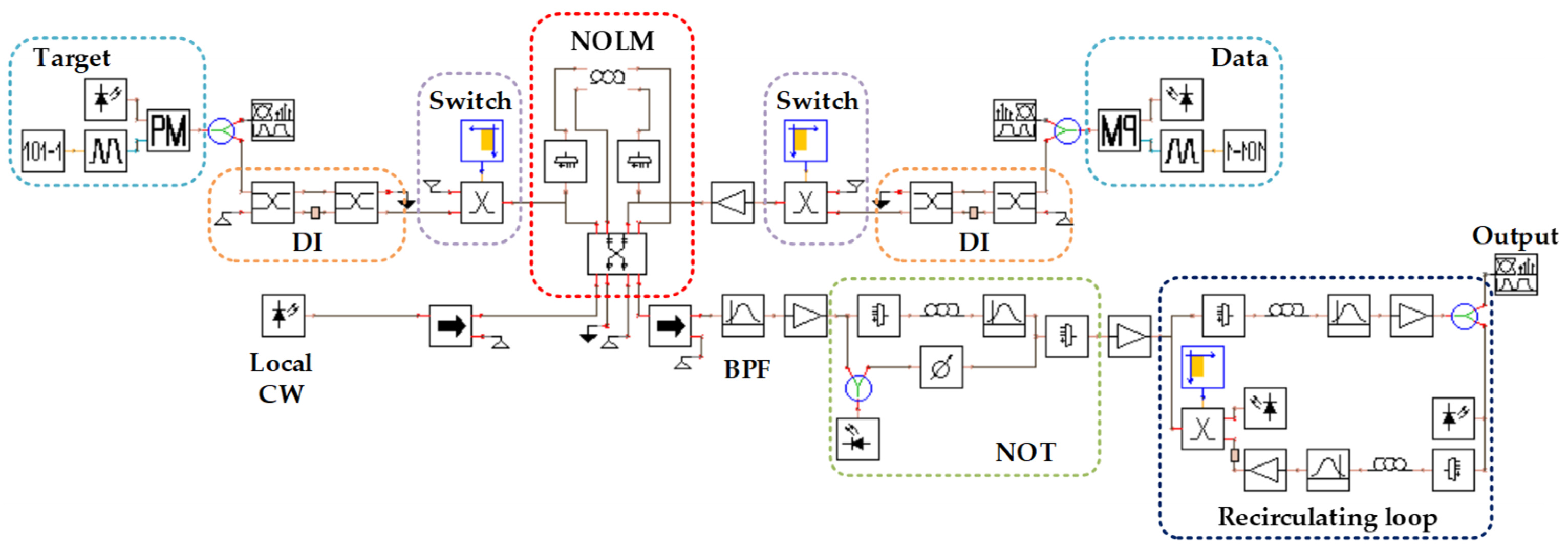
This section presents the simulation setup and parameter settings of the proposed all-optical pattern recognition system using VPItransmissionMaker 8.5. The data rate is set to 100 Gbps in our simulation considering the parameters of HNLF used in the system.
Figure 5 shows the numerical simulation setup of the proposed system, and the parameter setting of various modules in simulation is displayed in
Table 1.
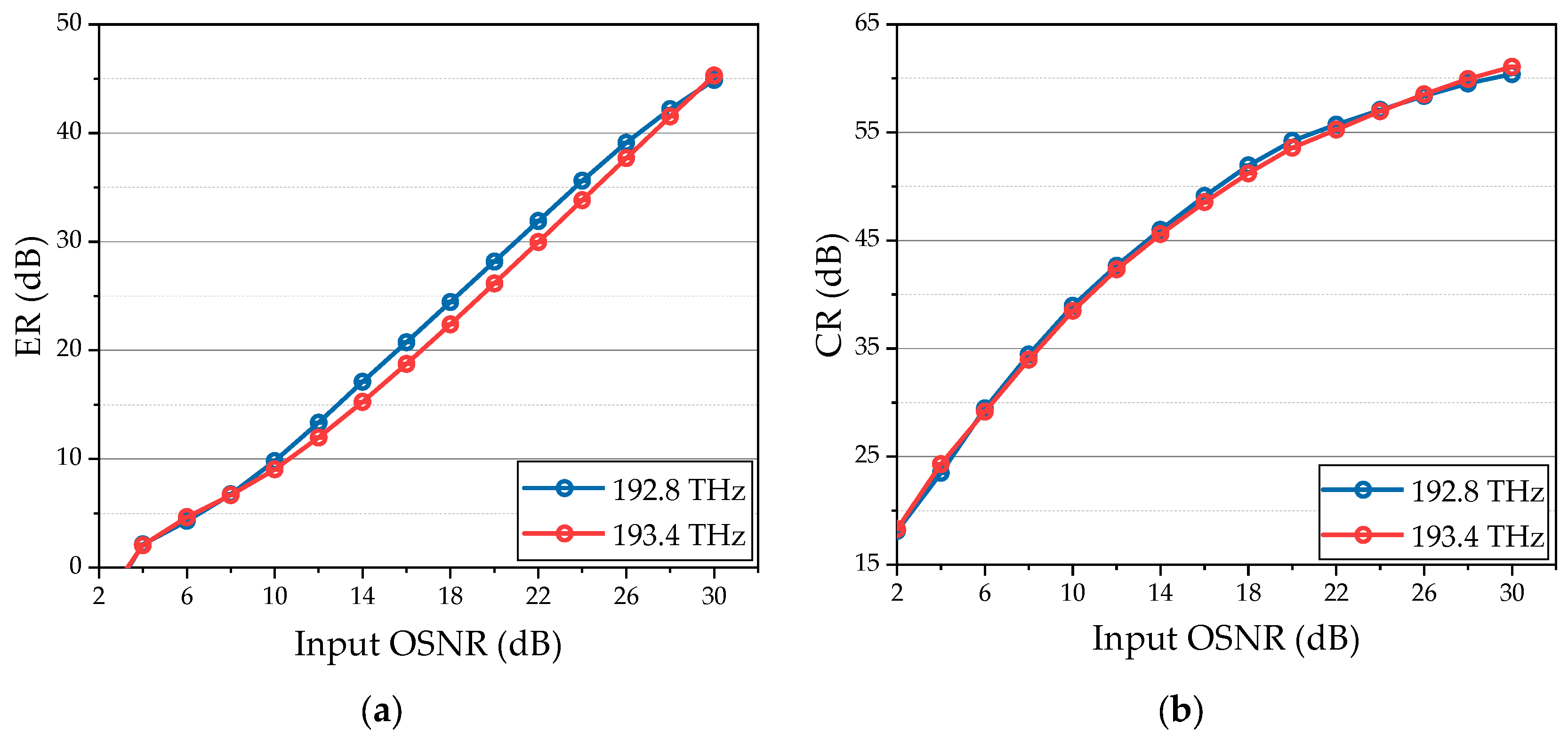
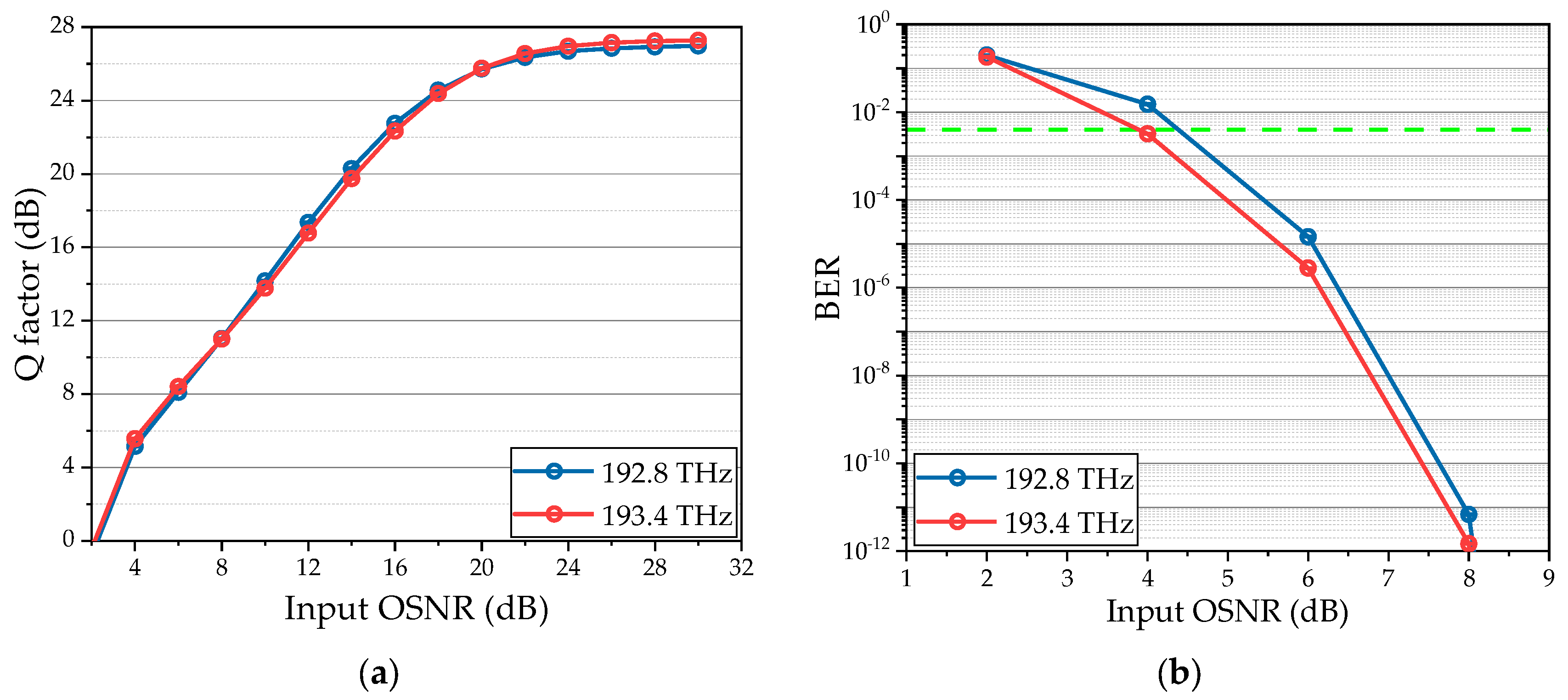
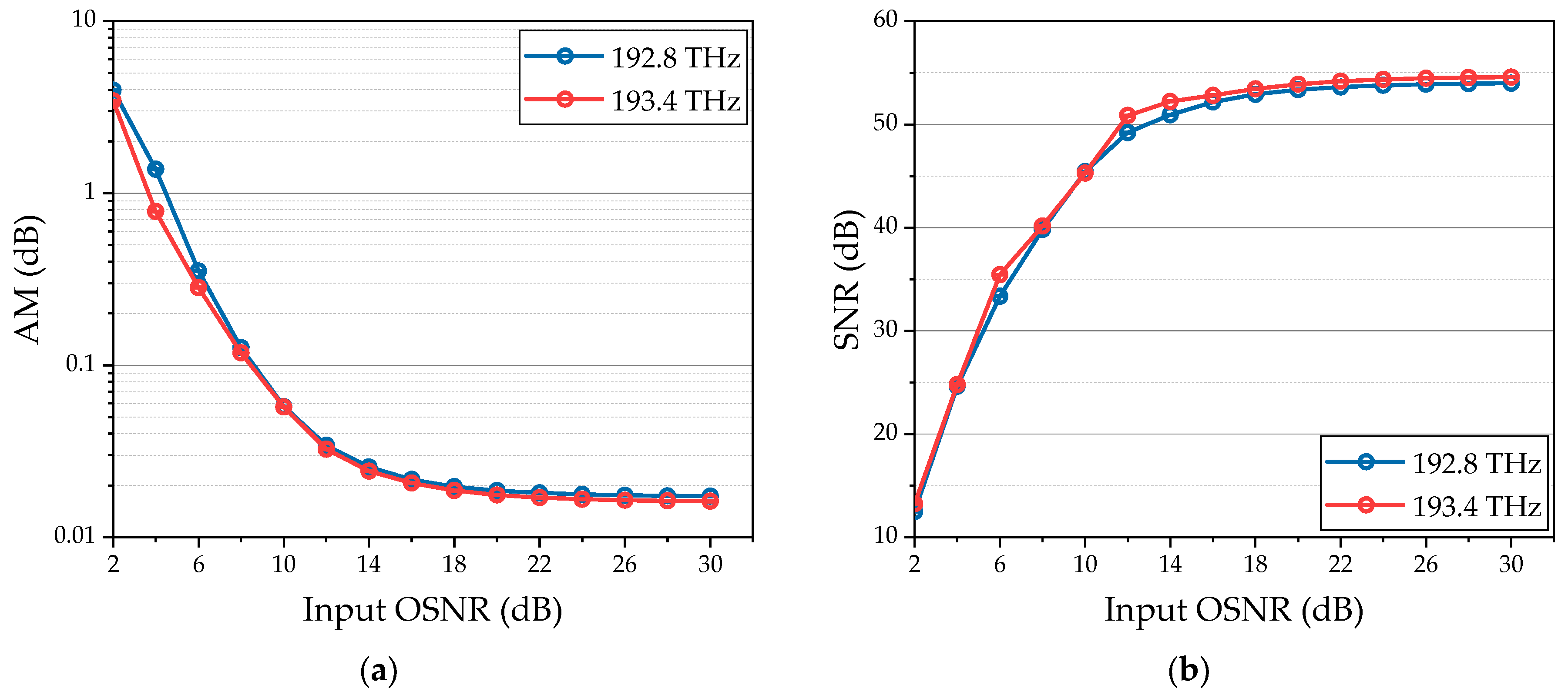
Data and Target: The incoming data and target sequence are represented by two synchronized BPSK signals, which are generated using predetermined data and ideal phase modulators. The input data stream is structured as a periodically replicated sequence, thereby avoiding the storage loop. The center frequency of the target is always set to 193.4 THz. To verify the performance of the system in processing the input data with tunable frequency, we set the center frequency of the input data to 192.8 THz and 193.4 THz in the simulation, which are symmetrical about the center frequency of the local CW.
DI: The DI module consists of two 50:50 couplers and an optical delay line (ODL). For the right DI following the input data, the delay time of the ODL is set to T, while for the left DI following the target, the delay time of the ODL is set to nT.
Switch: The switch module selects one of two input signals through a control signal. In the first loop, the optical switch selects a null source to pass through. After that, it selects the output of DI to pass through, so as to eliminate the interference brought about by the initial state. The output of the right switch is amplified by 20.06 dB and 20.02 dB when the center frequencies of the input data are 192.8 THz and 193.4 THz, respectively.
NOLM: The NOLM is constructed by a bidirectional 50:50 coupler, two multiplexers, and a bidirectional HNLF. First, the local CW with a center frequency of 193.1 THz passes through the unidirectional isolator and bidirectional coupler sequentially to generate the clockwise and counterclockwise carriers. Then, the input data and the counterclockwise carrier are injected into the HNLF through the right multiplexer. Meanwhile, the target and the clockwise carrier are injected through the left multiplexer. Subsequently, these two carriers are coherently interfered in the bidirectional coupler.
NOT: The output of the NOLM passes through another unidirectional isolator and a BPF with a center frequency of 193.1 THz to obtain the bit-recognition result. Before entering the NOT gate, an amplifier with a gain of 18.19 dB is used to increase the power of the bit-recognition result. Meanwhile, the probe with an average power of 0.5 mW at 192.8 THz inside the NOT gate is split into two branches. Then, the bit-recognition result, which serves as the pump, and the upper branch of the probe propagate through the following HNLF to generate the XPM effect. The upper branch of the probe experiences a phase shift induced by XPM, with its magnitude linearly dependent on the pump power. Thus, we modify the gain of the amplifier to achieve an XPM-induced phase shift of π. For the lower branch of the probe, an attenuator is used to match the output power of the upper branch. When the bit-recognition result is a logic “1”, destructive interference occurs at the multiplexer, resulting in an output of logic “0”. Conversely, when the bit-recognition result is a logic “0”, constructive interference occurs at the multiplexer, leading to an output of logic “1”. Therefore, the NOT gate is completed.
Loop: The output of the NOT gate is amplified by 4.97 dB using EDFA, and then enters the recirculating loop to complete the pattern recognition for variable target length. As the result of the first loop can be ignored, in the second loop, the initializing pulse which has an average power of 6 mW at 193.1 THz enters the subsequent AND gate with the output of the NOT gate. The AND gate operation is implemented by the FWM process within the HNLF. The output from this AND gate is then filtered using a BPF with a center frequency set at 192.5 THz. To ensure the power levels are consistent prior to entering the regenerator, an amplifier with a gain of 20.43 dB is employed. The regenerator itself also utilizes the FWM process within the HNLF to achieve frequency conversion. In the regenerator, the pump’s center frequency is 192.8 THz, and it maintains an average power of 6 mW. After interacting inside the HNLF, a BPF with a center frequency of 193.1 THz is utilized to extract the frequency-converted signal. An amplifier with a gain of 20.48 dB is positioned downstream. Finally, the output from the regenerator is fed back to the input of the AND gate after a delay of (n + 1)T. Upon completion of the second loop, the input to this AND gate is switched to the output of the regenerator via a control signal.
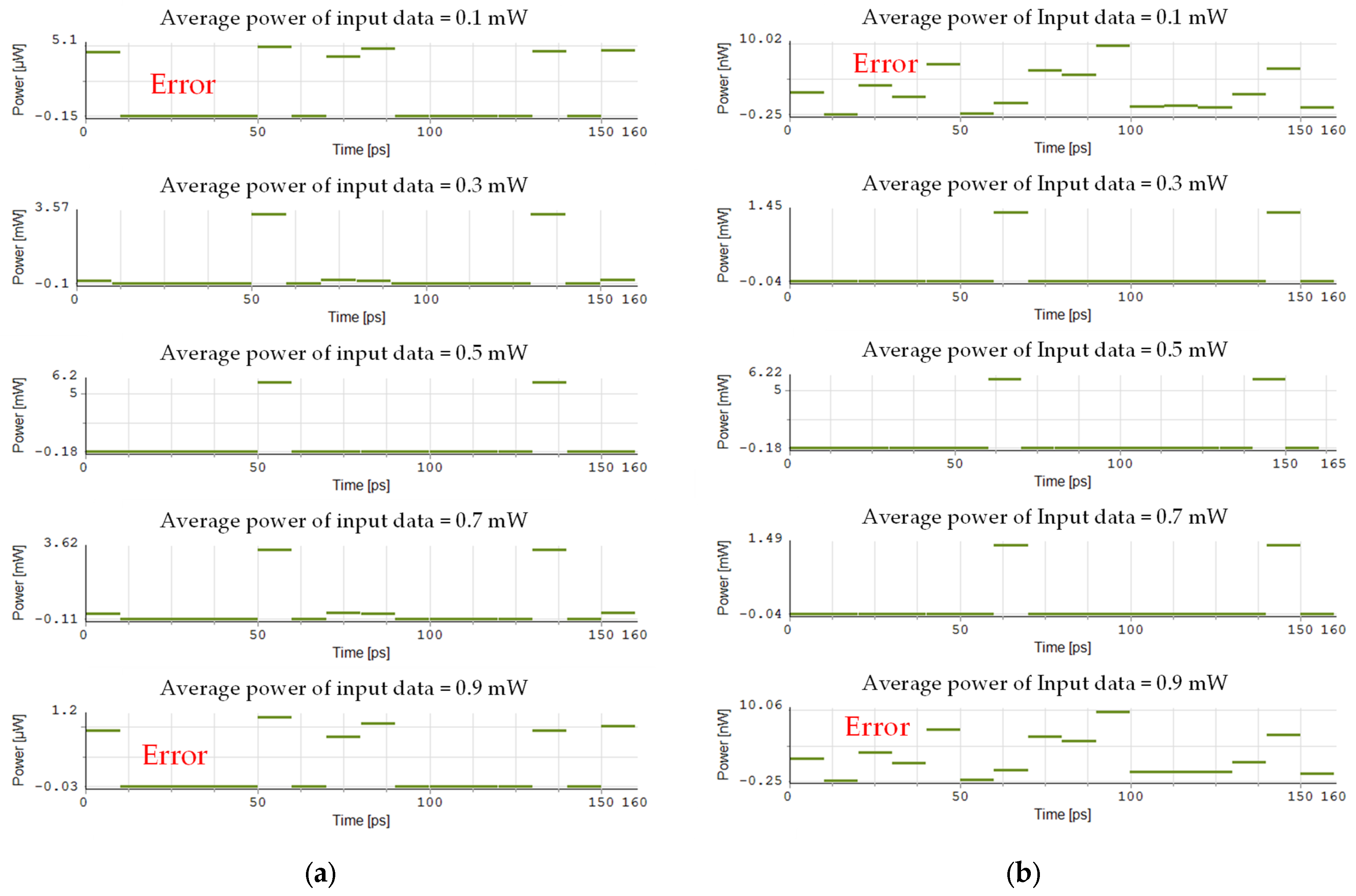
During the parameter selection process, we first clarified the average power of the input data. Considering the signal power transmitted in optical fibers, it is justified to set the value to 0.5 mW [
17]. For the input signal frequencies, we chose 192.8 THz and 193.4 THz, which are centered around 193.1 THz. As the standard WDM channel spacing is 100 GHz, by setting the frequency spacing to 300 GHz, we ensure compatibility with existing optical network equipment while meeting the spectral occupancy requirements of high-data-rate signals. Moreover, the larger spacing reduces inter-channel crosstalk and mitigates nonlinear interference. Nonlinear effects such as FWM in HNLF can introduce noise. The 300 GHz spacing ensures that FWM-generated products are away from the main signal frequencies, allowing them to be easily filtered out by BPFs with a bandwidth of 100 GHz, thereby preserving signal integrity. The input frequencies of 192.8 THz and 193.4 THz are symmetrically distributed around the local CW frequency of 193.1 THz. This symmetric configuration aims to validate the system’s performance at dual frequency points and test its adaptability to tunable frequency. Through this symmetric frequency arrangement, the system’s flexibility in dynamically tunable WDM networks can be effectively evaluated. Subsequently, we set the parameters of the HNLF and chose a relatively lower power of 1 mW for the local CW [
18]. However, during simulations, we observed that the phase shift induced by the XPM effect in the bidirectional HNLF failed to reach π. Therefore, we gradually increased the nonlinear coefficient to approximately 29 W⁻
1 × km⁻
1 [
19]. We found that this value ensures significant XPM effects at 100 Gbps while avoiding signal distortion caused by excessive nonlinearity. The power of the target was determined through iterative optimization, ensuring that the XPM-induced phase shift reaches π when the left DI output is high, thereby completing signal reloading in the NOLM. Similarly, the gain of the EDFA before the input signal enters the NOLM was precisely calibrated to achieve a π-phase shift when the right DI output is high. All lasers were configured with a linewidth of 100 KHz, aligning with the typical ideal linewidth for CW lasers in coherent optical communication systems [
22]. Additionally, setting this value to 100 KHz can effectively reduce the impact of phase noise on the system. All gain values of EDFA and output powers were optimized through multiple iterative simulations. By properly setting the gain value, the output signal power is maintained at the required level to drive subsequent logic operations.


