Abstract
With the rapid growth of data center demand driven by AI, high-speed optical modules (such as 800G and 1.6T) have become critical components. Traditional 800G modules face issues such as complex processes and large sizes due to the separate packaging of EML chips, AlN substrates, and capacitors. This study proposes a high-speed EML module based on silicon integration, where resistors, capacitors, and AuSn soldering areas are integrated onto the silicon substrate, enabling the bonding of the EML chip, reducing packaging costs, and enhancing scalability. Key achievements include: the development of a 100G EML chip; the fabrication of a high-speed silicon integrated carrier; successful Chip-on-Carrier (COC) packaging and testing, with a laser output power of 10 mW, extinction ratio of 10 dB, and bandwidth greater than 40 GHz; and reliability verified through 500 h of aging tests. This study provides an expandable solution for next-generation high-speed optical interconnects.
1. Introduction
With the rapid development of information technology, global data demand has surged, placing higher requirements on data transmission in data centers, computing clusters, and other fields [1,2,3]. To meet these needs, optical modules have become a core technology for high-speed data transmission between data centers [4,5,6]. Traditional Distributed Feedback Laser (DFB) laser chips are unable to meet the short-term demands for both high bandwidth performance and high yield, making it necessary to consider using III-V electroabsorption modulated laser chips to achieve high-speed transmission at a single wavelength of 100G [7]. However, existing 800G modules (Figure 1) use separate EML chips, AlN substrates, and large capacitors, which result in high thermal load and assembly complexity (Figure 2), and fail to fully meet the future demands for even higher transmission rates [8,9].
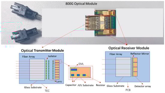
Figure 1.
Current physical samples of 800G optical modules and schematic diagrams of optical transceiver modules.
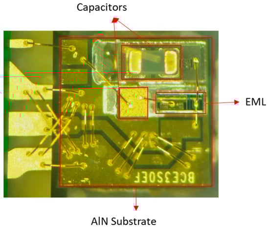
Figure 2.
The current 800G optical module typical product, the COC physical image of the optical transmission module.
Building on this, the paper proposes a high-speed EML module solution based on silicon integration technology [10]. By integrating matching resistors and capacitors onto the silicon substrate (Figure 3), this approach reduces power consumption and packaging complexity compared to traditional optical modules, while also lowering manufacturing costs [11,12]. Moreover, most researchers primarily focus on improving the modulation rate of EML chips [13,14,15], with limited exploration of performance enhancement through optimization of supporting silicon-integrated carriers. Seok-Jun Yun et al. [16] fabricated DML/EML-based subassembly modules, achieving chip-to-chip optical butt coupling via direct waveguide connections between silicon-based AWG chips and commercial DML or EML devices. The EML-based subassembly exhibited exceptional optical characteristics under external optical reflection, including a side-mode suppression ratio (SMSR) exceeding 50 dB and superior optical eye diagrams during 112-Gbps PAM4 operation. Notably, their optimization methodology diverges fundamentally from the approach proposed in this work. By optimizing the transmission characteristics of the silicon-integrated carrier, our in-house-developed EML demonstrates an experimentally validated bandwidth surpassing 40 GHz. Experimental validation shows that our optical module performs excellently in 100G single-wavelength transmission, with low power consumption and high stability, meeting the demands of modern optical communication technologies for high speed, low power consumption, and high reliability.
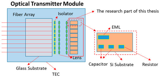
Figure 3.
Schematic diagram of the module part in this study.
2. Materials and Methods
2.1. EML Laser Chip Design and Fabrication
Based on the performance requirements for EMLs in data centers, a process for developing EML chips with a butt-joint structure is proposed (Figure 4) [17]. The main steps include: (1) material and structural design for the DFB and electroabsorption Modulator (EAM) regions; (2) process development before the butt-joint epitaxy to ensure a smooth growth interface; (3) material growth and characterization, including multiple rounds of butt-joint epitaxy and grating epitaxy; (4) chip fabrication, ensuring ultra-low reflectivity coating and reliability; (5) chip packaging and testing, including COC packaging and optimization of RF matching. The most critical aspects of this process are the butt-joint technique, selective epitaxy, and quality control during multiple epitaxial growth stages.
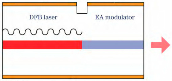
Figure 4.
Schematic diagram of the EML laser structure design.
The EML laser adopts a butt-joint structure design, with the DFB laser region generating a stable single longitudinal mode. The electroabsorption (EA) modulation region is directly grown in contact with the laser, optimizing the performance of both the DFB and EA regions [18,19].
The butt-joint process is critical for the structural design of laser diode (LD) lasers and EAM modulators, as poor alignment can lead to increased optical loss and reduced power. This process requires strict control over the morphology and thickness of the epitaxial substrate, especially during multiple epitaxial growth stages. To stabilize the surface structure, a combination of dry etching and wet etching is used. During the epitaxial process, impurities on the substrate surface can affect crystal quality. The EML process is more difficult to control than traditional DFB epitaxy, making substrate treatment particularly important. By optimizing the secondary epitaxy process, crystal quality was significantly improved, avoiding defects. A comparison of the epitaxial quality before and after optimization shows that the improved process greatly enhances crystal quality (Figure 5).
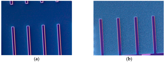
Figure 5.
Comparative characterization of surface crystal quality before and after epitaxial pre-treatment optimization ((a): pre-optimization; (b): post-optimization).
Selective epitaxy is a technique used to grow epitaxial material within a defined area on the substrate surface [20]. By depositing SiO2 or SiN to form a mask and using photolithography to open windows, the epitaxy is confined to the semiconductor surface within the window region. The dielectric mask induces lateral gas diffusion and surface quality migration effects, which can impact the growth morphology. The protrusion length of the SiO2 mask and the etching step depth have a significant influence on the growth morphology. If the mask protrusion is too short, it can cause the dielectric to wrap around, affecting gas diffusion; if it is too long, it can hinder sidewall growth. To address this, experiments were conducted with different substrate aspect ratios for the buried structure, and the buried cross-sectional Scanning Electron Microscope (SEM) results are shown in the figure below.
As seen in Figure 6, the smaller the substrate’s depth-to-width ratio, the larger the voids beneath the dielectric mask [21]. When the depth-to-width ratio is around 2, the SiO2 mask fills the area completely, resulting in the best morphology. Since the vapor phase reactants only deposit in the window region, a concentration gradient exists between the window and the masked area, causing group III reactants to diffuse from the masked area to the window (Figure 7). This increases the growth rate in the window region and alters the solid solution composition. Therefore, the growth rate can be estimated based on the layout area.
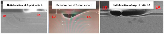
Figure 6.
Experiment on the morphological changes of buried structures with different depth-to-width ratios.
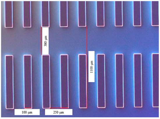
Figure 7.
Substrate morphology of the selective area epitaxy pattern.
The grating-embedded secondary epitaxy process is a key step in the epitaxial growth of EML lasers, primarily controlling the grating morphology and the density of epitaxial defects. These factors directly impact the laser’s threshold current, efficiency, side-mode suppression ratio, and stability. Experiments optimizing the secondary epitaxy growth conditions show that as the bake temperature increases, the morphology of the grating etching grooves changes. At lower temperatures, a well-maintained rectangular shape is preserved, while at higher temperatures, the shape becomes wavy, significantly damaging the rectangularity, as shown in the Figure 8.
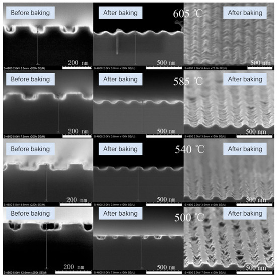
Figure 8.
The impact of different temperatures on the material growth process and mass transport phenomena.
To maintain the grating morphology, we chose a lower bake temperature and grew a partial InP filler layer. However, growing InP at low temperatures reduces crystal quality and affects the subsequent epitaxial layer growth. To ensure the quality of the epitaxial crystal, we adopted a two-step growth process: first, a low-temperature bake and filling of the grating grooves, followed by an increase in temperature to continue growing the remaining InP. This process ultimately results in a DFB secondary epitaxial wafer with a good grating morphology, as shown in Figure 9.
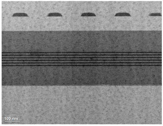
Figure 9.
Cross-sectional TEM image of the DFB epitaxial wafer after the two-step growth process.
Compared to conventional DFB lasers, EML lasers require 4–6 epitaxial growth steps. The EML laser used in this study is integrated with both the laser and modulator and features a ridge waveguide structure, incorporating four epitaxial layers: LD epitaxy, grating-embedded epitaxy, EA integration epitaxy, and the TOP layer epitaxy [21,22,23]. To improve the internal performance consistency and reliability, the processes of grating fabrication, etching, metallization, and coating were optimized. Figure 10 illustrates the fabrication process and key steps for the EML chip.
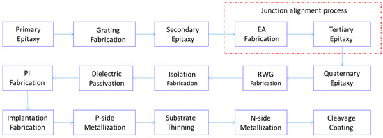
Figure 10.
Fabrication process flow of the EML laser.
2.2. Design and Process Implementation of High-Speed Si-Based Integrated Substrates
EML lasers are typically integrated on AlN or Si substrates to form a COC structure, achieving high performance, miniaturization, and high reliability. To enable circuit matching, the substrate typically incorporates key structures such as resistors, capacitors, high-speed signal lines, and AuSn solder. AlN ceramic substrates lack electrical functionality and rely on metallization and subsequent assembly of circuit components, whereas Si materials offer greater scalability [24,25], allowing direct fabrication of structures like resistors and capacitors, providing a significant advantage.
Based on the parameters of the existing Si-based platform, a 55 GHz high-frequency EML packaging substrate with an RF structure was designed. This structure employs a Coplanar Waveguide (CPW) [26] transmission line without a ground plane, and the transmission line model was established based on the actual material structure of the silicon substrate (Figure 11). By optimizing the physical parameters of the transmission line, a structure meeting the design requirements was developed. On this basis, bond pads for the chip and PCB were added, and their S-parameter characteristics were calculated to meet the design specifications. Finally, a complete transmission model for the EML, integrated substrate, and PCB was established [27,28,29]. The pad positions and bonding methods were optimized, resulting in excellent transmission characteristics with a transmission loss of ≤1.2 dB at 50 GHz and a return loss of ≤−12.41 dB, meeting the design requirements. Based on this, the overall structure of the high-speed silicon integrated substrate was designed.
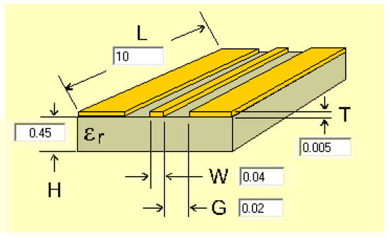
Figure 11.
Basic parameters of the CPW transmission line model.
Based on the simulation results, the matching circuit for the high-speed Si-based integrated substrate requires two capacitors (3 nF and 10 nF), one resistor (50 Ω), one high-speed signal line, and one AuSn solder pad with an area of 0.593 × 0.31 mm2. These structures must be integrated onto a Si-based substrate with dimensions of 1.8 × 0.85 mm2. The final layout design of the high-speed Si-based integrated substrate is shown below (Figure 12). The layout structure of the high-speed Si-based substrate is depicted, with the locations of the high-density capacitors, polycrystalline silicon resistors, high-speed signal lines, and AuSn solder pads marked in the diagram.
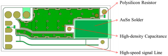
Figure 12.
Layout structure of the high-speed Si-based substrate.
Based on the design of high-density capacitors, the following process flow was developed, as shown in the diagram (Figure 13). In this section, the high-speed Si-based substrate was successfully fabricated according to the outlined process flow. Additionally, key process parameters and yield were optimized to enhance output, and the related process improvements have been proven to be applicable in industrial settings, offering significant value. The process flow outlined below resulted in the process structure shown in Figure 14.

Figure 13.
High-speed Si-based substrate process flow.
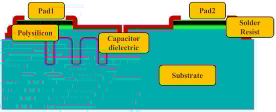
Figure 14.
Structure diagram of the high-speed Si-based substrate.
2.3. COC Packaging Technology
COC is an integrated circuit packaging technology that reduces packaging area and improves signal transmission efficiency by stacking and interconnecting multiple chips. Using a self-developed high-speed matching silicon carrier, the EML laser chip is attached and bonded through a eutectic bonding process. The LD and EA electrodes are connected to the carrier’s transmission lines and circuits via gold wire bonding. The alignment and positioning accuracy during the assembly process were optimized by comparing key feature areas of the chip and carrier, which improved chip recognition and the consistency of die placement. Batch testing results show that after optimization, the relative position of the chip and carrier is within ±2.5 μm in the X direction, ±7.5 μm in the Y direction, and the relative angular deviation is ±0.5°, demonstrating good consistency and meeting mass production requirements. The schematic diagram of the entire COC packaging is illustrated in Figure 15, while the physical photograph is shown in Figure 16.
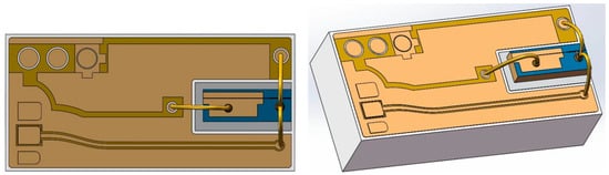
Figure 15.
COC packaging diagram: (Left), top view; (Right), side view.
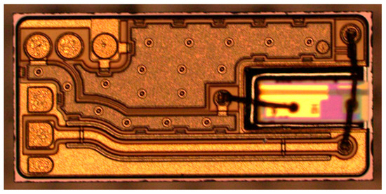
Figure 16.
COC packaging physical image.
3. Results
3.1. Performance Testing of the EML Chip
The COC optoelectronic parameter testing was conducted at 55 °C, with separate power scans applied to the LD and EA to test their optical and electrical performance. For the LD test, a 0–130 mA DC linear sweep was used, monitoring the LD voltage and EML output optical power to generate the power–current–voltage curve. From this, parameters such as threshold current (Ith), output optical power (Po), and slope efficiency (SE) were calculated. The test results show that at 100 mA, the EML’s output optical power reaches 10 mW, meeting the power requirements for 400G/800G modules in data centers. The extinction ratio test was conducted at an LD current of 100 mA, with the EA voltage scanned from −3 V to 0 V, resulting in a static extinction ratio of approximately 10 dB, which meets the requirements. However, further optimization of the EA extinction characteristics could be made to lower the module’s Vpp level. The COC output optical characteristics and extinction ratio plots are shown below (Figure 17).
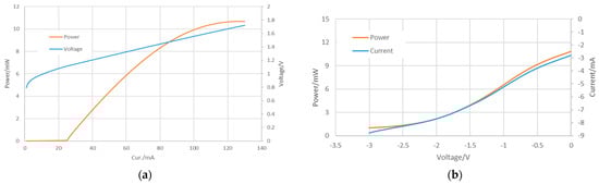
Figure 17.
(a) COC output optical characteristics plot; (b) COC extinction ratio characteristics plot.
3.2. COC Packaging Stability Test
COC high-temperature aging involves applying the rated current and voltage in a high-temperature environment to simulate real-world usage conditions and assess the device’s long-term reliability and stability, while screening for early failures. Key factors influencing aging include the precision and stability of the temperature, current, and voltage control, as well as the aging duration. Reliability validation was performed on the improved COC, monitoring the changes in Ith and Po. The test conditions were set at 85 °C and 1.5 times the operating current. Reliability validation was simultaneously performed on over 20 chips. Figure 18 presents the aging test results of over 20 chips over 500 h. The variation rates of (a) threshold current (Ith) and (b) output power (Po) during aging are both within an absolute value of 10%, demonstrating the stable reliability of the EML chips and packaging process.
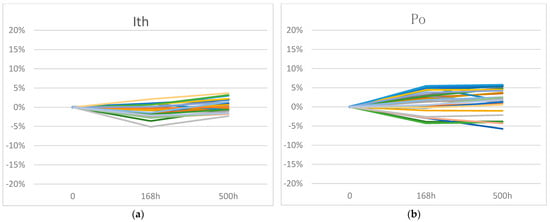
Figure 18.
COC reliability validation: (a) variation in Ith and (b) variation in Po over 500 h.
4. Discussion
The output light is analyzed spectrally using grating and other beam-splitting elements to measure the light intensity at different wavelengths, determine the center wavelength, and ensure that the laser output wavelength falls within the specified range. This ensures proper wavelength matching with optical communication system components, such as optical fibers and photodetectors, reducing transmission losses and dispersion. At the same time, the main mode and side mode light powers are measured to calculate the side-mode suppression ratio (SMSR), which evaluates the spectral purity of the laser. A high SMSR helps improve signal quality and transmission stability. The COC test spectrum is shown below (Figure 19).
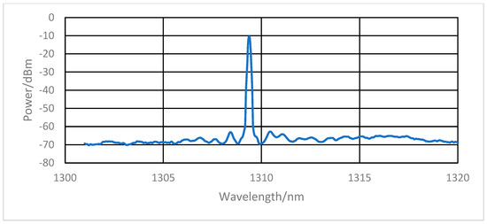
Figure 19.
COC test spectral characteristics plot.
The COC bandwidth test was conducted on a temperature-controlled hot plate at 55 °C. First, the Ground-Signal-Ground (GSG) probe was connected to the GSG pad of the COC, and an external probe was used to apply power to the LD P electrode to ensure the EML chip was properly powered (LD 100 mA, EA −1.0 V). Then, a tapered optical fiber was coupled to the output port of the EML chip, and its position was adjusted to ensure the coupling power exceeded 1 mW. Finally, the optical vector network analyzer was set to electro-optic mode, and the RF signal was transmitted to the EML chip via a coaxial cable (Figure 20). The signal was converted to an optical signal and returned to the optical vector network analyzer, which processed the data to generate the bandwidth test curve (S-parameter curve). The physical photograph of the COC bandwidth testing is shown in Figure 21.
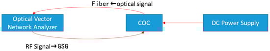
Figure 20.
EML bandwidth test link schematic.
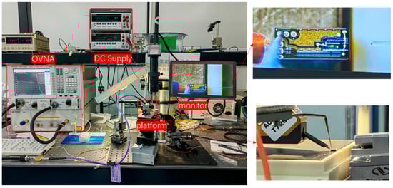
Figure 21.
EML bandwidth test link hardware image.
The test results are shown in the Figure 22. The S21 parameter is tested to be greater than 40 GHz at −3 dB. For a 56G EML, the typical requirement is for a bandwidth greater than 30 GHz, and for 100 Gbps transmission using Pulse Amplitude Modulation (PAM) modulation, the bandwidth is generally required to reach 35 GHz. The test results indicate that the developed EML chip meets the transmission rate requirement for single-channel 100 Gbps.
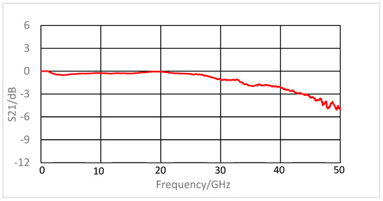
Figure 22.
EML bandwidth test S21 parameter plot.
5. Conclusions
This study successfully developed a high-speed EML module based on silicon-integrated technology, addressing key issues in current 800G modules with innovative solutions. These advancements significantly reduce packaging costs while enhancing overall performance and reliability. By optimizing the silicon carrier design, resistors and capacitors were directly integrated, packaging costs were significantly reduced, and stable performance with a capacitance density of 26.83 nF/mm2 and a resistance value of 50 Ω was achieved. The design and development of the EML chip overcame challenges in junction alignment processes, ultimately achieving an output power of 10 mW, an extinction ratio of 10 dB, and a bandwidth greater than 40 GHz, meeting the 100 Gbps transmission rate requirement. Through 500 h of high-temperature aging testing, the variations in Ith and Po remained within 10%, demonstrating the reliability and long-term stability of the EML module in high-temperature environments. The test results show that the EML module developed in this study offers high power output and stable electrical performance, providing reliable technical functioning.
Author Contributions
Conceptualization, L.L. and C.G.; methodology, Y.X. and L.L.; software, L.L.; validation, L.L. and W.Y.; investigation, L.L., Y.X. and W.W.; resources, C.G. and Y.Z.; data curation, L.L. and X.C.; writing—original draft preparation, L.L.; writing—review and editing, Y.X.; supervision, Q.W. and C.D.; funding acquisition, X.X. All authors have read and agreed to the published version of the manuscript.
Funding
Thanks for the support of the project “Ultra-high resolution optical fiber spectrum analyzer (No.2023YFF0715800)” and “Research on Key Technologies for Improving Stability and Reliability of Optoelectronic CT Measurement in Ultra High Voltage Scenarios”, project number 5700-202420251A-1-1-ZN.
Institutional Review Board Statement
Not applicable.
Informed Consent Statement
Not applicable.
Data Availability Statement
Data are contained within the article.
Conflicts of Interest
Author Liang Li was employed by the company China Electronics Technology Group Corporation Industrial Basic Research Institute, Shijiazhuang. The remaining authors declare that the research was conducted in the absence of any commercial or financial relationships that could be construed as a potential conflict of interest.
References
- Tausanovitch, N. Analysis of Hardware Technologies Required for Artificial Intelligence (AI). Integr. Circuit Appl. 2018, 35, 3. [Google Scholar] [CrossRef]
- Hunt, E.B. Artificial Intelligence; Academic Press: New York, NY, USA, 2014. [Google Scholar]
- Fetzer, J.H. What Is Artificial Intelligence? Artificial Intelligence: Its Scope and Limits; Springer Netherlands: Dordrecht, The Netherlands, 1990; pp. 3–27. [Google Scholar]
- Wei, L.P. Development trends and prospects of optical communication technology. Telecommun. Sci. 2003, 19, 5. [Google Scholar] [CrossRef]
- Nakazawa, M.; Kikuchi, K.; Miyazaki, T. High Spectral Density Optical Communication Technologies; Springer Science & Business Media: Berlin/Heidelberg, Germany, 2010. [Google Scholar]
- Wang, H.T.; Zhang, P.H.; Su, Z. 800 Gbit/s optical module technology and applications. ZTE Commun. 2021, 27, 40–46. [Google Scholar]
- Wu, B.; Zhao, W.; Zhang, H. Progress of 800 Gb/s optical module and optoelectronic chips technology. In Proceedings of the Optoelectronic Devices and Integration XI. SPIE, Online, 5–11 December 2022; Volume 12314, pp. 65–68. [Google Scholar]
- Xiang, P.; Song, X.; Zheng, Y.; Ye, Y.; Liu, C.G.; Mu, L. Research and design of 800 Gbit/s PAM4 LR8 10 km optical module. In Proceedings of the 2022 7th International Conference on Communication, Image and Signal Processing (CCISP), Chengdu, China, 18–20 November 2022; pp. 18–22. [Google Scholar]
- Nishimura, K.; Asakura, H.; Yamauchi, S.; Suzuki, T.; Nakai, Y.; Yamaguchi, Y.; Kageyama, T.; Mitaki, M.; Endo, Y.; Naoe, K. 225-Gb/s PAM4 Operation Using Lumped-Electrode-Type EA-DFB Laser for 5 and 10-km Transmission with Low TDECQ. In Proceedings of the Optical Fiber Communication Conference, San Diego, CA, USA, 16–21 February 1997. [Google Scholar]
- Zhu, Y.X.; Zhang, X.; Li, Y.; Li, J.; Lin, X.; Tang, X.; Luo, Y.; Lu, H.; Gai, S. Analysis of the development trends in the global optical chip field. World Sci. Technol. Res. Dev. 2024, 46, 705–719. [Google Scholar]
- Sun, C.Z.; Yang, S.H.; Xiong, B.; Wang, J.; Luo, Y. Research progress on high-speed electro-absorption modulated lasers. Chin. J. Lasers 2020, 47, 701002-1. [Google Scholar]
- Song, J.J.; Zhang, Q.; Li, L. Study on junction alignment process of electro-absorption modulated laser (EML). Integr. Circuit Appl. 2023, 40, 8–10. [Google Scholar]
- Uchiyama, A.; Okuda, S.; Tsuji, T.; Hokama, Y.; Shirao, M.; Abe, K.; Yamatoya, T.; Yamauchi, Y. Demonstration of 155 Gbaud PAM4 and PAM6 EML with Narrow High-Mesa EA Modulator for 400 Gbps per Lane Transmission. In Proceedings of the Optical Fiber Communication Conference, San Diego, CA, USA, 24–28 March 2024; p. Tu2D-1. [Google Scholar]
- Huang, J.J.-S.; Chang, H.S.; Hsu, Y.-C.; Chiu, A.; Fang, Z.; Yu, C.-Y.; Hsiang, S. 212Gbps high-power EML for 800G artificial intelligence optical transmissions. Comp. Opt. Photonics 2024, 1, 001–005. [Google Scholar] [CrossRef]
- Bhasker, P.; Arora, S.; Robertson, A.; Ni, A.; McCaully, T.; Bloch, J.; Johnson, J.E. 75 GHz BW Ultra-High Speed O-band Hybrid CMBH Ridge EMLs for Next Generation Ethernet. In Proceedings of the ECOC 2024, 50th European Conference on Optical Communication, Frankfurt, Germany, 22–26 September 2024; pp. 596–598. [Google Scholar]
- Yun, S.J.; Han, Y.T.; Kim, S.T.; Shin, J.U.; Park, S.H.; Lee, D.H.; Lee, S.Y.; Baek, Y. Optical subassembly modules using light sources butt-coupled with silica-based PLC. IEEE Photonics Technol. Lett. 2019, 32, 132–135. [Google Scholar]
- Kobayashi, W.; Arai, M.; Yamanaka, T.; Fujiwara, N.; Fujisawa, T.; Tadokoro, T.; Tsuzuki, K.; Kondo, Y.; Kano, F. Design and fabrication of 10-/40-Gb/s, uncooled electroabsorption modulator integrated DFB laser with butt-joint structure. J. Light. Technol. 2009, 28, 164–171. [Google Scholar]
- Sun, Y.X.; Yang, Z.Q.; Jia, H.Y.; Yu, J.; Li, D. Optimization design of a novel electro-absorption modulated laser. Study Opt. Commun. 2023, 49, 69–78. [Google Scholar]
- Liu, G.L.; Wang, X.; Xu, G.Y.; Chen, W.; Zhang, B.; Zhou, F.; Zhang, J.; Wang, X.; Zhu, H. Selective area epitaxy fabrication of monolithic integrated single ridge electro-absorption modulated DFB laser. Chin. J. Lasers 2001, 28, 321–324. [Google Scholar]
- Han, W. Design of Material Structure and Epitaxial Growth for 1.55 μm High-Speed Lasers. Master’s Thesis, Hebei University of Technology, Tianjin, China, 2006. [Google Scholar]
- Brook, J.; Dandliker, R. Submicrometer holographic photolithography. Solid State Technol. 1989, 32, 91–95. [Google Scholar]
- Pease, R.F.W. Electron beam lithography. Contemp. Phys. 1981, 22, 265–290. [Google Scholar] [CrossRef]
- Lan, H.; Ding, Y. Nanoimprint Lithography; InTech: Rijeka, Croatia, 2010. [Google Scholar]
- Meng, X.F.; Zhu, H. Research progress on AlN substrate materials. Ceram. Res. Vocat. Educ. 2003, 1, 41–45. [Google Scholar]
- Lederer, D.; Raskin, J.P. Substrate loss mechanisms for microstrip and CPW transmission lines on lossy silicon wafers. Solid-State Electron. 2003, 47, 1927–1936. [Google Scholar]
- Kim, J.; Jung, B.; Cheung, P.; Harjani, R. Novel CMOS low-loss transmission line structure. In Proceedings of the 2004 IEEE Radio and Wireless Conference (IEEE Cat. No. 04TH8746), Atlanta, GA, USA, 22 September 2004; pp. 235–238. [Google Scholar]
- Yun, H.G.; Choi, K.S.; Kwon, Y.H.; Choe, J.S.; Moon, J.T. Fabrication and characteristics of 40-Gb/s traveling-wave electroabsorption modulator-integrated DFB laser modules. IEEE Trans. Adv. Packag. 2008, 31, 351–356. [Google Scholar]
- Shirao, M.; Ohata, N.; Yasui, N.; Uto, K.; Fukao, T.; Hatta, T.; Aruga, H.; Mizuochi, T. A 1.55 μm 40 Gbps EML TOSA Employing a Novel FPC Connection. J. Light. Technol. 2014, 32, 3344–3350. [Google Scholar]
- Xu, C.; Xu, Y.Z.; Zhao, Y.; Lu, K.; Liu, W.; Fan, S.; Zou, H.; Liu, W. High-Frequency Modeling and Optimization of E/O Response and Reflection Characteristics of 40 Gb/s EML Module for Optical Transmitters. ETRI J. 2012, 34, 361–368. [Google Scholar]
Disclaimer/Publisher’s Note: The statements, opinions and data contained in all publications are solely those of the individual author(s) and contributor(s) and not of MDPI and/or the editor(s). MDPI and/or the editor(s) disclaim responsibility for any injury to people or property resulting from any ideas, methods, instructions or products referred to in the content. |
© 2025 by the authors. Licensee MDPI, Basel, Switzerland. This article is an open access article distributed under the terms and conditions of the Creative Commons Attribution (CC BY) license (https://creativecommons.org/licenses/by/4.0/).