Communication

Novel Spectrum Inversion-Based Double-Sideband Modulation with Low Complexity for a Self-Coherent Detection System

School of Computer and Communication Engineering, University of Science and Technology Beijing, Beijing 100083, China
*
Author to whom correspondence should be addressed.
Photonics 2025, 12(4), 302; https://doi.org/10.3390/photonics12040302
Submission received: 9 March 2025 / Revised: 21 March 2025 / Accepted: 24 March 2025 / Published: 26 March 2025
(This article belongs to the Special Issue Exploring Optical Fiber Communications: Technology and Applications)

Abstract

:
In high-capacity and short-reach applications, double-sideband self-coherent detection (DSB-SCD) has garnered significant attention due to its ability to recover optical fields of DSB signals without requiring a local oscillator. However, DSB-SCD is fundamentally constrained by the non-ideal receiver transfer function, necessitating a guard band between the carrier and signal. While the conventional twin-single-sideband (twin-SSB) modulation scheme addresses this requirement, it incurs substantial implementation complexity. In this paper, we propose a spectrum inversion-based double-sideband (SI-DSB) modulation scheme, where spectral inversion shifts the DSB signal to the high-frequency region, creating a guard band around the zero frequency. After photodetector detection, baseband signal recovery is achieved through subsequent spectral inversion. Compared with the twin-SSB modulation scheme, this approach significantly reduces DSP complexity. The simulation exploration two modulation formats of pulse–amplitude modulation and quadrature-amplitude modulation, demonstrating a comparable system performance between SI-DSB and twin-SSB modulation schemes. We also illustrate the parameter optimization process for the SI-DSB modulation scheme, including carrier-to-signal power ratio and guard band. Furthermore, validation with three FADD receivers further demonstrates the superior performance of the proposed SI-DSB modulation in DSB-SCD systems.

1. Introduction

The rapid expansion of mobile internet, virtual reality, and cloud computing applications has driven the demand for high-capacity, ultra-high-speed fiber optical communication systems. For short-reach optical communications, intensity modulation and direct detection (IM-DD) remains a dominant scheme owing to its cost-effectiveness and implementation simplicity [1,2]. Nevertheless, dispersion-induced power fading in IM-DD systems has been a key challenge, which may necessitate digital compensation through precise optical field reconstruction. To address this challenge, self-coherent detection (SCD) systems have emerged as a promising alternative, achieving low-complexity optical field recovery while maintaining cost efficiency [3,4].
In the SCD system, a modulation signal is co-transmitted with the unmodulated carrier at the transmitter and obtains the desired signal after direct detection at the receiver side [5,6,7,8]. The expensive local oscillator laser is removed, which is not the case in coherent detection. Moreover, since the signal and the carrier are derived from the same laser, the SCD does not require frequency offset estimation (FOE) or phase recovery (PR). Based on the relative position of the modulation signal and the carrier, the SCD can be categorized into single-sideband self-coherent detection and double-sideband self-coherent detection (DSB-SCD). The latter implements double-sideband modulation and achieves higher electrical spectrum efficiency.
Several DSB-SCD receiver architectures have garnered significant research attention, including the carrier-assisted differential detection (CADD) receiver [9,10,11,12,13], asymmetric self-coherent detection (ASCD) [14], carrier-assisted phase retrieval (CAPR) [15], and filter-assisted direct detection (FADD) [16]. But the above schemes are limited by non-ideal receiver transfer function. The twin single-sideband (twin-SSB) technique is usually used to insert a guard band to mitigate the system performance degradation caused by the receiver transfer function. However, this approach requires the separate processing of two independent signals in digital signal processing (DSP), resulting in a high level of complexity. In addition, the twin-SSB modulation scheme is designed for self-coherent detection where a guard band is required, which is less universal.
In this paper, we propose a spectrum inversion-based double-sideband (SI-DSB) modulation scheme for the DSB-SCD to achieve the reservation of a guard band around the zero frequency. The SI-DSB modulation scheme incorporates dual-stage spectral inversion processes: the initial inversion shifts the DSB signal to the high-frequency region, creating a guard band around the zero frequency. Reverse inversion is subsequently applied after the FADD-based DSB-SCD receivers to restore the baseband signal. Based on single-carrier pulse–amplitude modulation (PAM) and quadrature-amplitude modulation (QAM) signals, the proposed SI-DSB modulation scheme is validated by co-simulation using MATLAB 2023a and VPItransmissionMaker 8.7. The simulation results demonstrate that the proposed SI-DSB modulation scheme achieves a comparable system performance to the conventional twin-SSB modulation scheme while maintaining lower DSP complexity.
The rest of this paper is organized as follows. In Section 2, the structure of the FADD receiver and the principle of the SI-DSB PAM/QAM modulation scheme are given. Section 3 presents the simulation results and offers corresponding explanations. Finally, Section 4 concludes the article.

2. Principle of the SI-DSB FADD

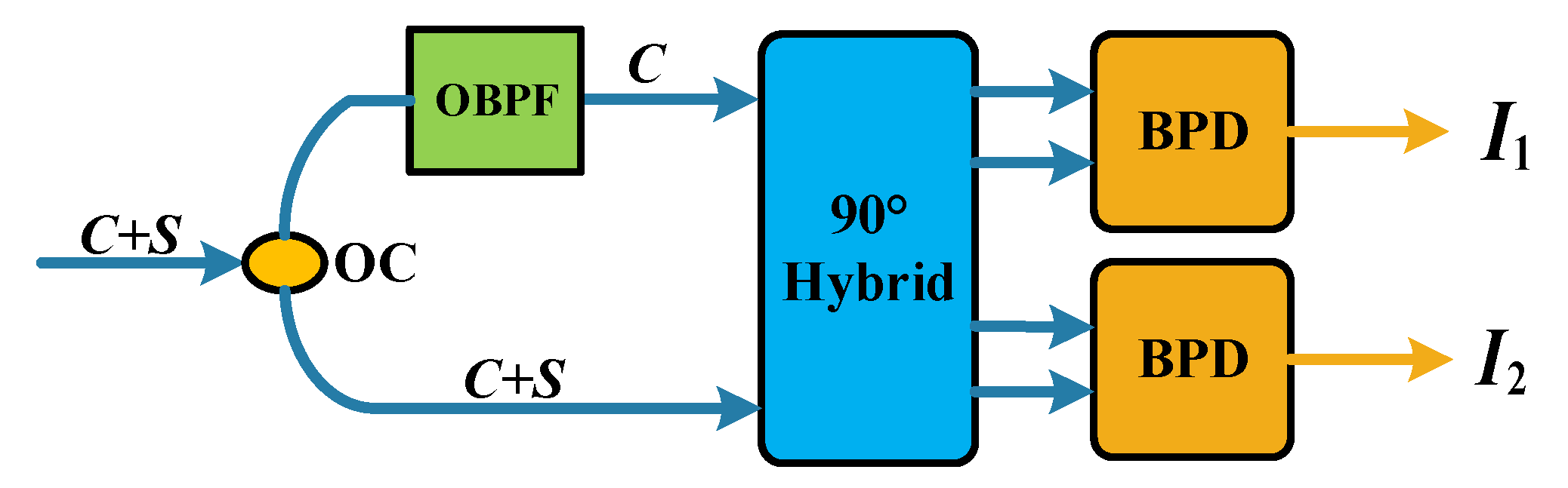
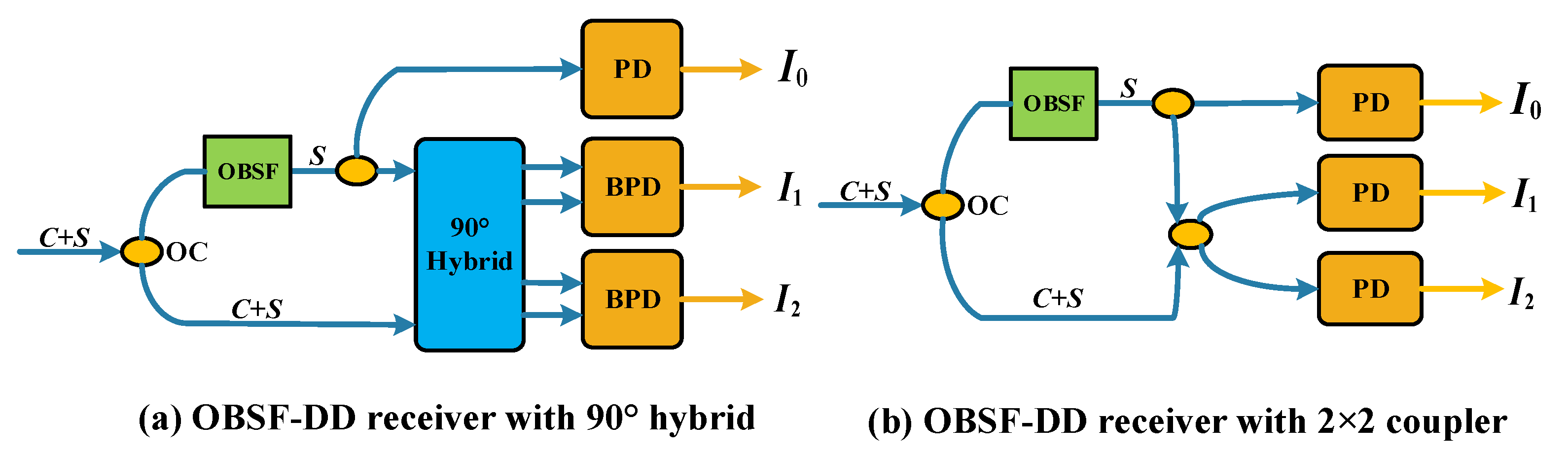
2.1. Structure of the FADD Receiver

The working principle of the FADD receiver [16] depicted in Figure 1 can be summarized as follows. The optical carrier and DSB signal are represented by C and S, respectively. The incoming optical signal is evenly divided into two branches. Subsequently, the unwanted DSB signals are suppressed by the optical bandpass filter (OBPF). Following detection by the photodetector (PD), the resulting photocurrents can be expressed as follows:
I 1 = 1 2 Re C + S / α * C + S
I 2 = 1 2 Im C + S / α * C + S
where Re{·} and Im{·} are the real and imaginary part operation, respectively. ‘*’ represents the conjugate, and α is defined as a relative amount of the unwanted signal power before and after OBPF. The complex signal R can be constructed using the two photocurrents.
R = I 1 + j I 2 = 1 2 C 2 + C S + C S / α + S 2 / α
When the guard band is large enough or the edge rolloff of the OBPF is sufficiently steep, the unwanted DSB signal can be effectively eliminated. Consequently, Equation (4) can be derived from Equation (3) by applying α .
R = 1 2 C 2 + C S
where the first term represents the DC term and the second term corresponds to the desired linear component. The DSB signal can be derived through the linear processing of Equation (4).
S = 1 C 2 R C 2
We observe that the FADD receiver can eliminate the effects of signal–signal beat interference (SSBI) distortion, thereby enabling the receiver to reconstruct the optical field of the signal with a relatively low carrier-to-signal power ratio (CSPR).

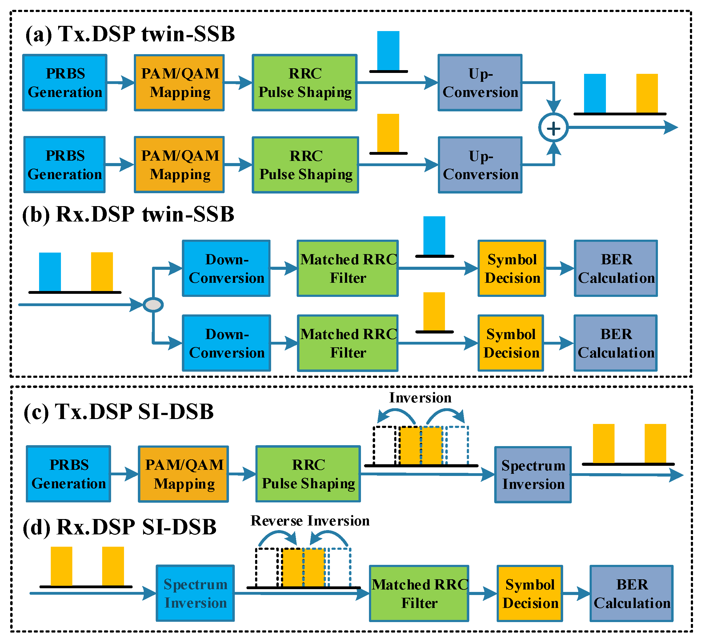
2.2. Principle of the PAM/QAM SI-DSB Modulation Scheme

In DSB-SCD, conventional DSB modulation becomes inapplicable due to the limitations of the non-ideal receiver transfer function. To address this issue, the twin-SSB modulation scheme is usually used in the DSB-SCD optical communication system. The transmit and receiver DSPs for the twin-DSB modulation scheme are shown in Figure 2a,b. At the transmitter, two independent pseudo-random binary sequence (PRBS) bit streams are generated and mapped to the PAM/QAM symbol sequence, respectively. After pulse shaping and up-conversion, the two signals are combined to obtain a twin-SSB signal. At the receiver, the received electrical signal is divided into two branches by a coupler, which are down-converted, respectively, and the two PRBSs are obtained by a matched root-raised cosine (RRC) filter and symbol decision. Obviously, the twin-SSB modulation scheme necessitates two-branch signal processing for DSB formation, introducing increased implementation complexity.
Therefore, we propose a simple SI-DSB modulation scheme, as shown in Figure 2c,d. At the transmitter, one pseudo-random binary sequence (PRBS) bit stream is generated and mapped to the PAM/QAM symbol sequence. The baseband signal is obtained after RRC pulse shaping. It should be noted that the achievable guard band via spectral inversion diminishes as the rolloff factor increases, according to the proportional relationship between rolloff factor and signal bandwidth. The spectrum inversion process involves reversing the odd bits of the original sequence x to obtain a new sequence, x′
X ( i ) = ( 1 ) i X ( i ) .
After spectrum inversion, the signal is shifted to the high-frequency region, achieving the reservation of the guard band. The guard band generated through spectrum inversion typically exhibits sufficient width, which can effectively mitigate various issues inherent to SCD systems. For example, the sharpness requirements of optical filter edges in the FADD receiver can be relaxed. In the CADD receiver, the SSBI exhibits an approximately triangular shape in the frequency domain, and its impact on the signal is reduced in the high-frequency region. As a result, a larger guard band can effectively mitigate SSBI, reducing the required CSPR.
At the receiver, the electrical signal output from the FADD receiver undergoes spectrum inversion, downgrading the high-frequency signals to low-frequency signals. Subsequently, the baseband signal is processed through a matched filter and symbol decision-making to obtain the final bit sequence. The proposed scheme only needs to add a spectrum inversion module to insert the guard band into the DSB signal, which significantly reduces the DSP complexity compared with the twin-SSB modulation scheme. Additionally, compared with the conventional PAM/QAM technique, the proposed SI-DSB modulation scheme only adds a spectrum inversion module, which is more universal.

3. Results and Discussion

3.1. Simulation Setup

To investigate the performance of the proposed SI-DSB modulation scheme, we conduct a simulation using VPItransmissionMaker and MATLAB. The transmission and modulation are conducted by VPI, while the DSP is implemented with MATLAB. The simulation system is shown in Figure 3, and the specific DSP flow is shown in Figure 2. The essential parameters for the simulation setup are listed in Table 1. At the transmitter, the PRBS bit streams are first mapped to generate the corresponding symbol sequences. Subsequently, the signal undergoes up-sampling two times and is then digitally shaped using a Root-Raised Cosine (RRC) filter. The optical signal is generated by spectrum inversion and IQ modulation. In the channel, only the effects of chromatic dispersion and additive white Gaussian noise (AWGN) are taken into account. At the receiver side, the FADD receiver is used to detect the signal. The baseband signal is then obtained by spectral inversion. Finally, the final bit sequences are obtained after matched RRC filter equalization, a symbolic decision. It is worth noting that the primary function of the equalization module is to reduce inter-symbol interference (ISI), which results from bandwidth limitations and chromatic dispersion.

3.2. Parameter Optimization of SI-DSB FADD

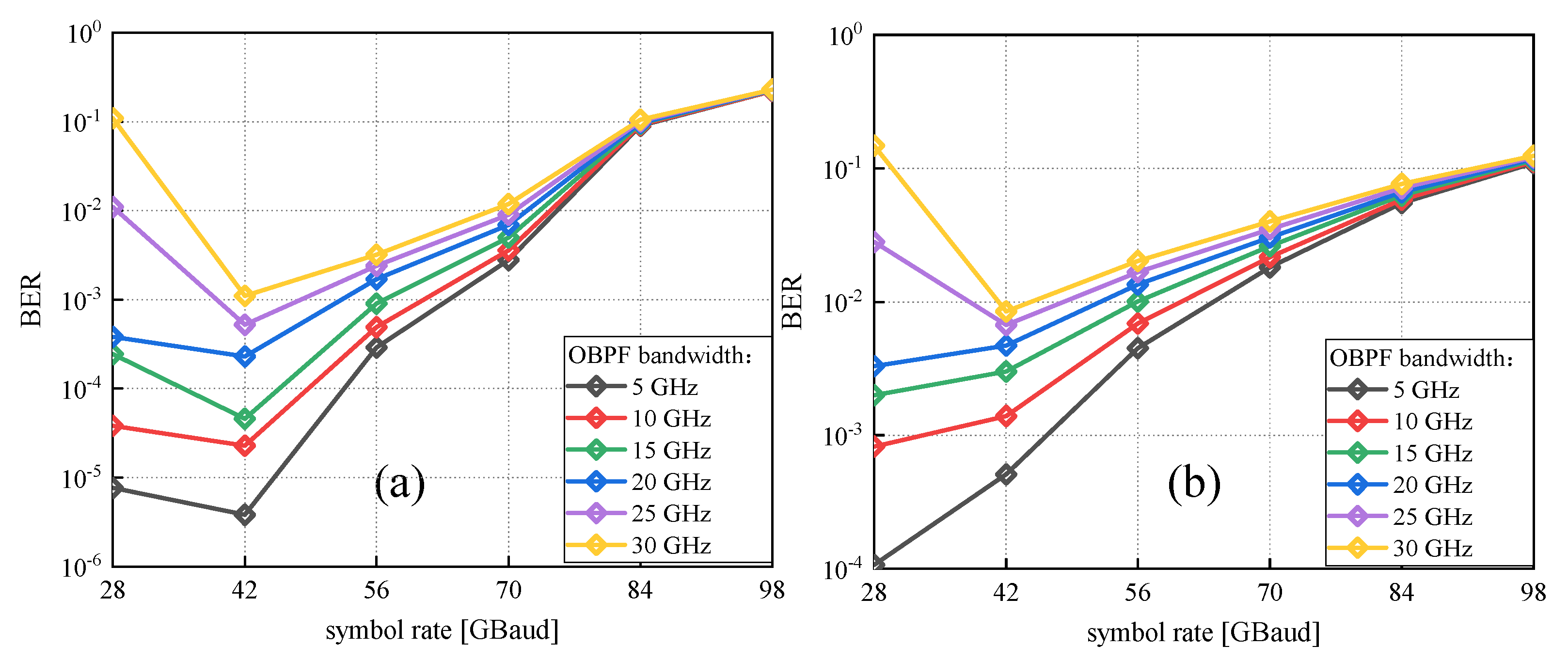
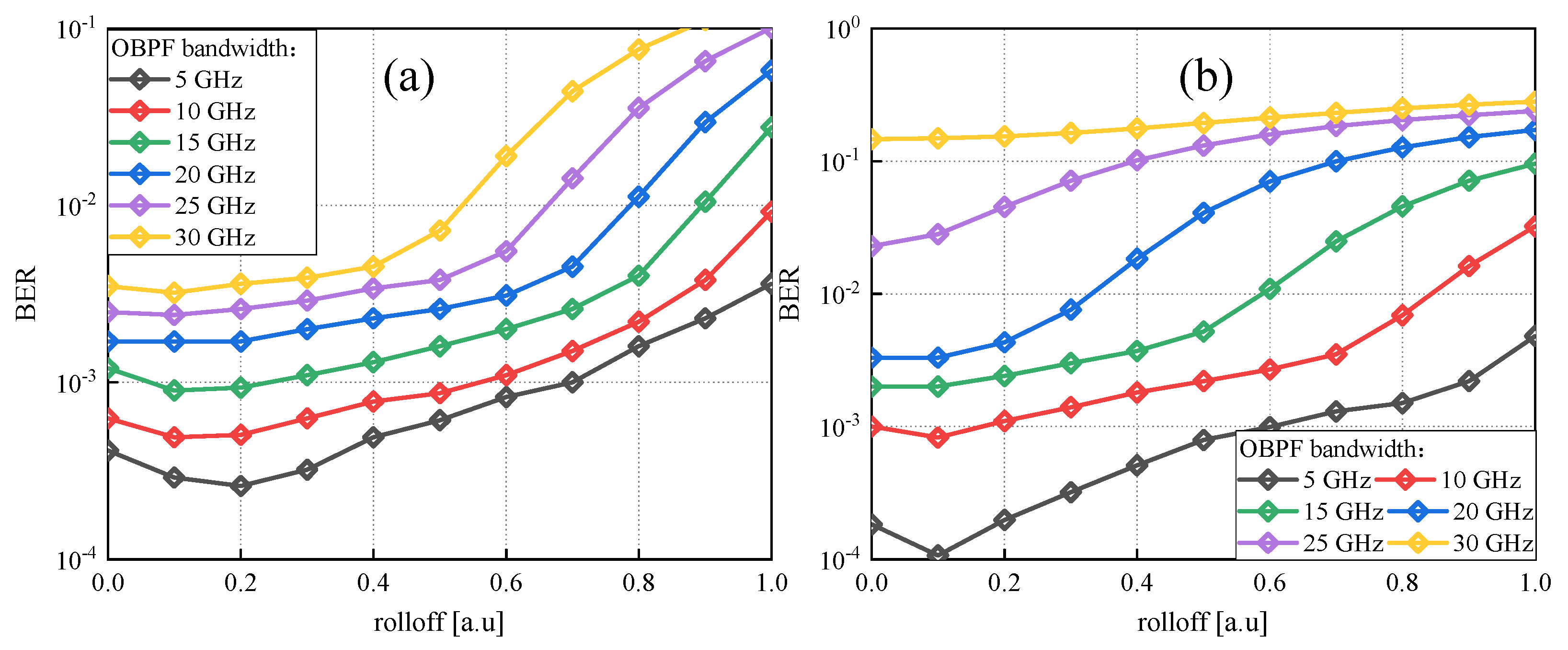
3.2.1. Guard Band of the SI-DSB Modulation
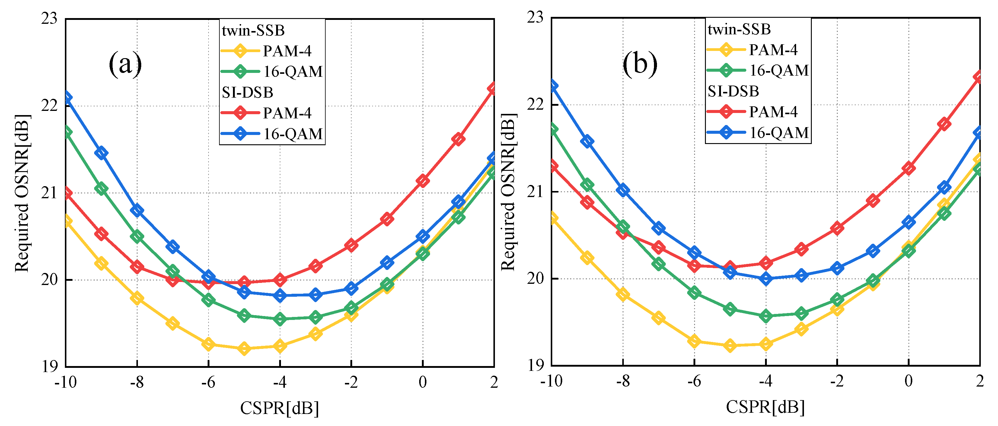
For proposed SI-DSB modulation, the guard band plays a key role in mitigating various damages in the SCD system. Therefore, the guard band needs to be deeply explored. In this paper, when the sample pre-symbol is fixed at two, the guard band of proposed SI-DSB modulation can be defined as the symbol rate × (1 − rolloff). As a result, the guard band is determined by the symbol rate and the rolloff factor. Figure 4a,b illustrate the performance of the system at different symbol rates for PAM-4 and 16-QAM, respectively. Notably, the OBPF bandwidth is swept from 5 GHz up to 30 GHz with a step size of 5 GHz. The parameter rolloff factor is fixed at 0.1, the OSNR is set to 23 dB, the received optical power (ROP) is −4 dBm, and their optimization and comprehensive analysis will be presented in the following sections. We find that the system performance deteriorates at a low symbol rate. The main reason is the symbol rate is positively correlated with the guard band. When the symbol rate is low, the smaller guard band prevents the FADD receiver from extracting a ‘clean’ carrier. As the symbol rate increases, the guard band becomes larger. Therefore, the BER performance is significantly improved. In addition, as the symbol rate increases further, the BER performance deteriorates sharply due to the limited system bandwidth. As a result, to avoid the impact of bandwidth limitation and ensure the adequacy of the guard band, the symbol rate for PAM-4 and 16-QAM is set to 28 GBaud and 56 GBaud, respectively, in the following simulations.
The rolloff factor is another important factor in determining the guard band of the SI-DSB signal. Figure 5a,b plot the bit-error rate (BER) versus rolloff for PAM-4 and 16-QAM signals at BTB, respectively. The OSNR is set to 23 dB, and the received optical power (ROP) is −4 dBm. Our findings are as follows: (1) Under the same rolloff factor, the system performance decreases with the increase in the OBPF bandwidth. This phenomenon may indicate that the greater the bandwidth, the more difficult it is to extract a “clean” carrier. (2) The system performance decreases with the increase in rolloff at the same OBPF bandwidth. This is because the guard band is negatively correlated with the rolloff factor. (3) The system’s performance is at its worst with a rolloff factor equal to one, as the guard band reduces to zero under this condition. (4) It is worth noting that to achieve the same information rate, the symbol rate of PAM-4 is set to twice that of 16-QAM. As a result, the PAM-4 modulation format demonstrates a superior system performance due to the larger guard band. The optimal system performance is observed when the OBPF bandwidth is 5 GHz, which is selected for the following simulations.

3.2.2. Optimal CSPR

A key parameter of the SCD system is the CSPR, which can be represented as C S P R = 10 log 10 ( P c a r r i e r / P s i g n a l ) ( d B ) . Herein, we tested the optimal CSPR of the SI-DSB modulation scheme, and the twin-SSB modulation scheme is also shown for comparison. Note that the symbol rate and the rolloff factor used by the twin-SSB modulation scheme are set to the same parameters as the SI-DSB modulation scheme. Thereby, both schemes occupy the same signal bandwidth and have the same size guard band. Figure 6 illustrates the required OSNR to meet a 7% forward error correction (FEC) threshold (BER = 3.8 × 10⁻³) for different CSPRs at BTB scenario and 80 km fiber transmission. The rolloff of the RRC filter is 0.1, and the OBPF bandwidth is 5 GHz. We find that the proposed SI-DSB and twin-SSB exhibit identical optimal CSPR. The optimized CSPR for PAM-4 is −4 dB and the 16-QAM is −5 dB, which will be used in the following simulations.

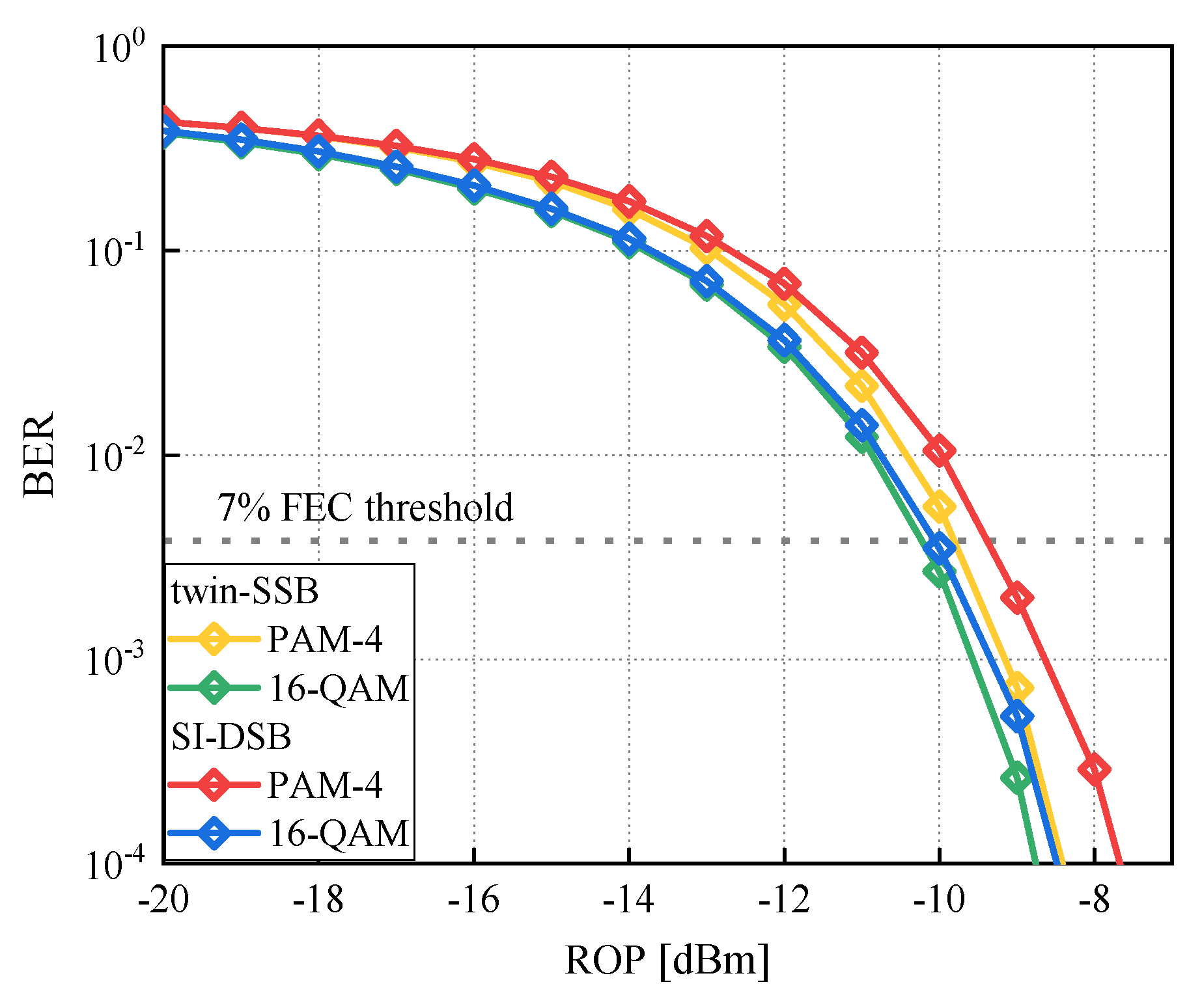
3.3. Comparison with Twin-SSB Modulation Scheme

In this subsection, the system performance of SI-DSB and twin-SSB modulation schemes is compared. Figure 7 displays the BER performance of SI-DSB and twin-SSB modulation schemes versus ROP at BTB. It is worth noting that the proposed SI-DSB and twin-SSB schemes each have a rolloff factor of 0.1, which occupies the same signal bandwidth. Under the two modulation formats, the proposed SI-DSB and twin-SSB modulation exhibit similar system performance. The slight performance difference is caused by bandwidth limitation. The proposed SI-DSB modulation scheme only equalizes one high-speed signal, while the twin-SSB modulation scheme requires two equalization algorithms to separately equalize the two low-speed signals. Therefore, while the complexity of the equalization algorithm is halved compared to the twin-SSB modulation scheme, the equalization performance is slightly reduced.

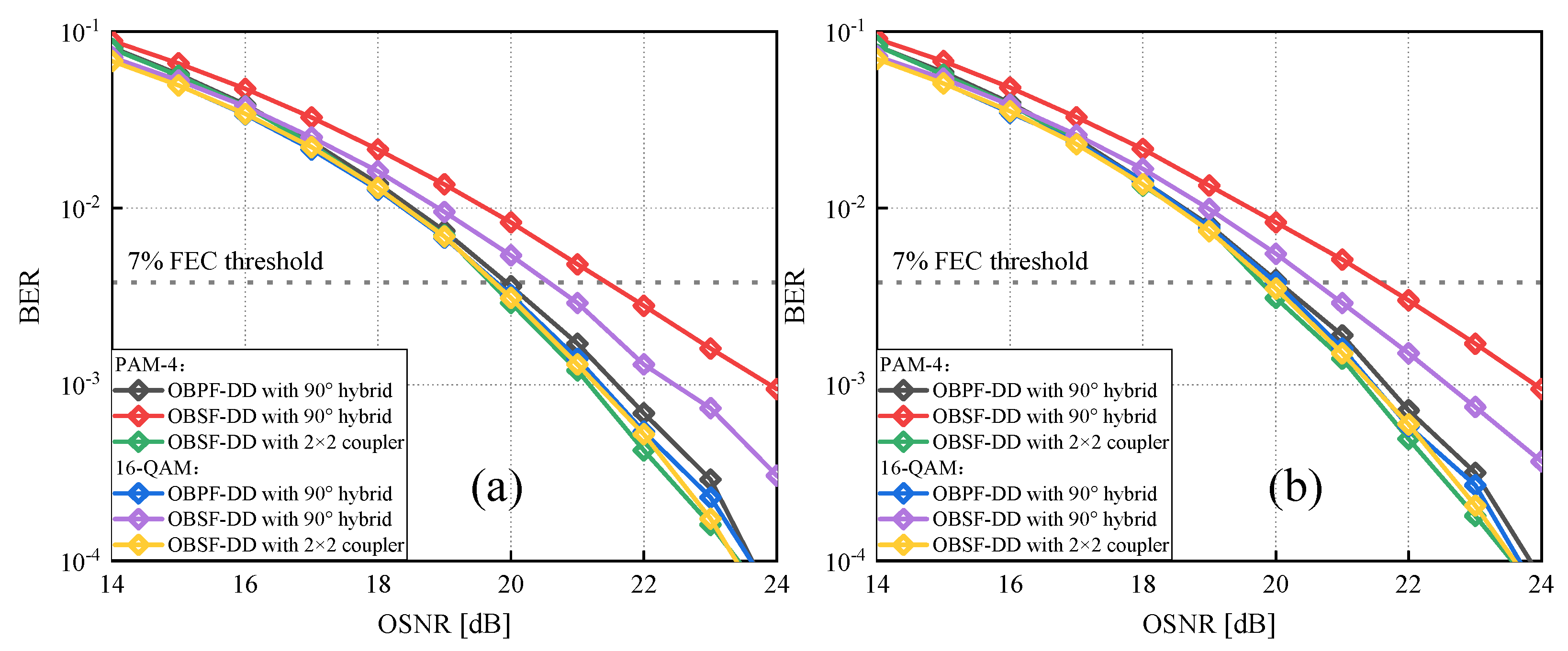
3.4. Performance Evaluation of SI-DSB FADD Systems

In previous work, three FADD receivers were proposed in [16]. In addition to the OBPF-DD with a 90° hybrid demonstrated in Figure 1, the other two receiver structures are shown in Figure 8. Herein, we conduct a comprehensive performance evaluation as shown in Figure 9. The ROP = −4 dBm, and the rolloff factor is 0.1. The performances of the three FADD receivers can be ranked in the following order: OBSF-DD with a 2 × 2 coupler, OBPF-DD with a 90° hybrid, and OBSF-DD with a 90° hybrid. The main reason for the difference in performance is the difference in the tolerance of electrical noise between the three schemes. In summary, the OBSF-DD with a 2 × 2 coupler not only has better system performance, but also can significantly reduce the complexity when combined with SI-DSB modulation.
The DSP of the proposed SI-DSB modulation scheme from offline program to chip implementation is related to the final power consumption and latency of the application-specific integrated circuit (ASIC) DSP chip. However, significant differences in power consumption and latency may occur when different design approaches are used to implement the same algorithm. Therefore, it is difficult to evaluate them in detail and professionally. However, the proposed SI-DSB modulation scheme demonstrates high compatibility with conventional DSB modulation schemes, significantly lowering barriers to practical deployment. In addition, with the exponential growth in the capabilities of complementary metal oxide-semiconductor (CMOS) integrated circuits, powerful DSP algorithms may be easy to implement in the near future without increasing power consumption and latency. Finally, we believe that the proposed SI-DSB can be applied to all DSB-SCD systems instead of twin-SSB modulation, and it is more suitable for cost-sensitive application scenarios.

4. Conclusions

In this paper, we have presented the SI-DSB modulation scheme, whose performance is primarily evaluated in the FADD receiver. However, it is also suitable for other SCD systems that require a guard band. We have shown the DSP flow diagram of the proposed SI-DSB and traditional twin-SSB modulation schemes, illustrating the advantages of the proposed scheme in terms of DSP complexity. Additionally, the parameters of the proposed SI-DSB FADD system are optimized, including guard band and CSPR. Subsequently, the system performances of the two modulation schemes are compared. To prove the universality of the proposed SI-DSB modulation scheme, the performance is evaluated in three FADD receivers. In summary, the proposed SI-DSB modulation scheme achieves a similar system performance to the twin-SSB modulation scheme, but the DSP complexity can be significantly reduced. We believe that the proposed SI-DSB modulation scheme is a feasible solution for DSB-SCD in cost-sensitive data center interconnect scenarios.

Author Contributions

Conceptualization, K.L. and J.H.; methodology, P.Q., J.H., X.Z., H.B., J.T. and K.L.; software, P.Q., J.H., H.B., X.Z. and J.T.; validation, P.Q., J.H., H.B. and X.Z.; writing—original draft preparation, P.Q.; writing—review and editing, authors contributed equally. All authors have read and agreed to the published version of the manuscript.

Funding

This research was funded by the National Natural Science Foundation of China NSFC, U22A2005 and 62201033; the Young Elite Scientists Sponsorship Program of CIC 2021QNRC001.

Institutional Review Board Statement

Not applicable.

Informed Consent Statement

Not applicable.

Data Availability Statement

The datasets generated and analyzed during the current study are available from the corresponding author on reasonable request.

Conflicts of Interest

The authors declare no conflicts of interest.

References

  1. Zhong, K.; Zhou, X.; Huo, J.; Yu, C.; Lu, C.; Lau, A.P.T. Digital signal processing for short-reach optical communications: A review of current technologies and future trends. J. Light. Technol. 2018, 36, 377–400. [Google Scholar] [CrossRef]
  2. Che, D.; Hu, Q.; Shieh, W. Linearization of direct detection optical channels using self-coherent subsystems. J. Light. Technol. 2016, 34, 516–524. [Google Scholar] [CrossRef]
  3. Lin, J.; Yan, L.; Yi, A.; Pan, Y.; Zhang, B.; Hu, Q.; Pan, W.; Luo, B. Integrated components and solutions for high-speed short-reach data transmission. Photonics 2021, 8, 77. [Google Scholar] [CrossRef]
  4. Winzer, P.J.; Essiambre, R.-J. Advanced Optical Modulation Formats. Proc. IEEE 2006, 94, 952–985. [Google Scholar] [CrossRef]
  5. Mecozzi, A.; Antonelli, C.; Shtaif, M. Kramers-kronig coherent receiver. Optica 2016, 3, 1220–1227. [Google Scholar] [CrossRef]
  6. Mecozzi, A.; Antonelli, C.; Shtaif, M. Kramers–Kronig receivers. Adv. Opt. Photon. 2019, 11, 480–517. [Google Scholar] [CrossRef]
  7. Sun, C.; Che, D.; Ji, H.; Shieh, W. Investigation of single-and multi-carrier modulation formats for Kramers–Kronig and SSBI iterative cancellation receivers. Opt. Lett. 2019, 44, 1785–1788. [Google Scholar] [PubMed]
  8. Le, S.T.; Schuh, K.; Chagnon, M.; Buchali, F.; Dischler, R.; Aref, V.; Buelow, H.; Engenhardt, K.M. 1.72Tb/s virtual-carrier assisted direct-detection transmission over 200 km. J. Light. Technol. 2018, 36, 1347–1353. [Google Scholar] [CrossRef]
  9. Shieh, W.; Sun, C.; Ji, H. Carrier-assisted differential detection. Light Sci. Appl. 2020, 9, 18–26. [Google Scholar] [CrossRef] [PubMed]
  10. Sun, C.; Ji, T.; Ji, H.; Xu, Z.; Shieh, W. Experimental demonstration of complex-valued DSB signal field recovery via direct detection. IEEE Photon. Technol. Lett. 2020, 32, 585–588. [Google Scholar] [CrossRef]
  11. Zhu, Y.; Li, L.; Fu, Y.; Hu, W. Symmetric carrier assisted differential detection receiver with low-complexity signal-signal beating interference mitigation. Opt. Express 2020, 28, 19008–19022. [Google Scholar] [CrossRef] [PubMed]
  12. Li, J.; An, S.; Ji, H.; Li, X.; Shieh, W.; Su, Y. Carrier-assisted differential detection with reduced guard band and high electrical spectral efficiency. Opt. Express 2021, 29, 33502–33511. [Google Scholar] [PubMed]
  13. Huang, Z.; Li, J.; Yu, X.; He, J.; Zhang, J.; Zhong, K.P.; Qin, Y. Joint signal-to-signal beat interference mitigation for the field recovery of symmetric carrier-assisted differential detection with low carrier-to-signal power ratio. Opt. Express 2024, 32, 18044–18054. [Google Scholar] [CrossRef] [PubMed]
  14. Li, X.; O’Sullivan, M.; Xing, Z.; Alam, M.; Mousa-Pasandi, M.E.; Plant, D.V. Asymmetric self-coherent detection. Opt. Express 2021, 29, 25412–25427. [Google Scholar] [CrossRef] [PubMed]
  15. Wu, Q.; Zhu, Y.; Hu, W. Carrier-assisted phase retrieval. J. Light. Technol. 2022, 40, 5583–5596. [Google Scholar] [CrossRef]
  16. Qin, P.; Huo, J.; Bai, C. Filter-assisted direct detection-based field recovery scheme for complex-valued double-sideband signals. Opt. Fiber Technol. 2024, 85, 103811. [Google Scholar] [CrossRef]
Figure 1. Structures of FADD receiver. OC: optical coupler. Balanced photodiode (BPD).
Photonics 12 00302 g001
Figure 2. Twin-SSB modulation scheme for (a) Tx.DSP; (b) Rx.DSP; SI-DSB modulation scheme for (c) Tx.DSP; (d) Rx.DSP.
Photonics 12 00302 g002
Figure 3. Simulation setup. SSMF: standard single-mode fiber.
Photonics 12 00302 g003
Figure 4. BER of different OBPF bandwidth of FADD receiver versus symbol rate in the BTB scenario for (a) PAM-4; (b) 16-QAM.
Photonics 12 00302 g004
Figure 5. BER of different OBPF bandwidth of the FADD receiver versus rolloff at BTB scenario for (a) PAM-4; (b) 16-QAM.
Photonics 12 00302 g005
Figure 6. Required OSNR versus CSPR with different schemes at (a) BTB scenario; (b) 80 km fiber transmission distance.
Photonics 12 00302 g006
Figure 7. Simulated received power sensitivity for different schemes in the BTB scenario.
Photonics 12 00302 g007
Figure 8. Structures of FADD receiver. (a) OBSF-DD with 90° hybrid; (b) OBSF-DD with 2 × 2 coupler.
Photonics 12 00302 g008
Figure 9. BER performance versus OSNR with different SI-DSB FADD schemes at (a) BTB scenario; (b) 80 km fiber transmission distance.
Photonics 12 00302 g009
Table 1. Simulation parameters.
ParametersValuesParametersValues
Sample pre-symbol2Bandwidth of RX33 GHz
Symbol length32,768OBPF transfer functionGaussian
Laser center frequency193.4 THzOBPF order4
Fiber length80 kmOBPF center frequency193.4 THz
Dispersion17 ps/nm/kmPD responsivity0.7 A/W
Dispersion slope0.08 ps/nm2/kmPD thermal noise10 pA/Hz1/2
Core area80 µmPD dark current3 × 10−9 A
Bandwidth of TX33 GHzPD shot noiseon
Disclaimer/Publisher’s Note: The statements, opinions and data contained in all publications are solely those of the individual author(s) and contributor(s) and not of MDPI and/or the editor(s). MDPI and/or the editor(s) disclaim responsibility for any injury to people or property resulting from any ideas, methods, instructions or products referred to in the content.

