1. Introduction
Spontaneous emission is a common phenomenon of atoms and molecules in nature, and is determined by the properties of atoms and molecules themselves. It plays a vital role in many fields, such as in laser technology, light-emitting diodes, solar cells, and quantum information processing [
1,
2,
3,
4]. Spontaneous emission had been considered as an inherent behavior of atoms or molecules for a long time before Purcell’s work. In 1946, Purcell first showed that spontaneous emission can be altered when the electromagnetic environment around an atom changes [
5]. Then, placing atoms near macroscopic objects became a regular method used to enhance spontaneous emission. In recent years, a large number of studies have shown that materials support surface plasmons (SPs), surface phonon polaritons (SPhPs), and hyperbolic phonon polaritons (HPhPs) play an important role in enhancing spontaneous emission and enabling strong light–matter interactions [
6]. Therefore, the most common way of modulating spontaneous emission is utilizing materials or structures, such as metamaterials [
7,
8], graphene-based structures [
9], or plasmonic nanostructures [
6,
10,
11], that can support surface polaritons. It has been found that when there are two or more atoms or molecules, the collective spontaneous emission can be larger or smaller than that of an individual atom because of the constructive or destructive interference between different atoms. Collective spontaneous emission is closely related to the relative positions of atoms. It is usually called superradiance or subradiance, depending on whether the collective spontaneous emission is enhanced or suppressed, respectively. Recently, superradiance has also been investigated in several different systems, such as plasmonic nanostructures [
12,
13,
14,
15] and graphene-based structures [
16,
17].
As an artificial material with novel optical characteristics and important applications, hyperbolic metamaterials (HMMs) have attracted extensive attention in the past two decades [
18,
19]. An HMM is a special type of anisotropic metamaterial whose permittivities parallel and vertical to the optical axis often have opposite signs, leading to a hyperbolic dispersion relation. The isofrequency contour (IFC) of the HMM takes the form of an open hyperboloid, which is different from the closed ellipsoidal IFC supported by the ordinary materials [
18,
19]. HMMs are widely used to achieve the broadband Purcell effect, because they can support hyperbolic polaritons, resulting in high-local-density photon states. In recent years, several methods have been proposed to fabricate HMMs, such as multilayer structures with alternating subwavelength metal–dielectric layers [
20], or metallic nanowires in a dielectric host [
21,
22,
23,
24,
25]. Among them, the high-
k mode is a feature of the multilayer structure and is generated by the near-field coupling of surface plasmas (SPs) excited by incident
p-polarized light at each metal–dielectric interface in the structure [
26,
27]. In addition, if the metal layers are substituted with a degenerate doped semiconductor, a new type of semiconductor HMM can be created [
28]. The semiconductor HMM can support hyperbolic plasmon polaritons (HPPs) with large wave vectors (high-
k waves). These semiconductor HMMs also have the distinct advantage of being able to adjust the plasma frequency by varying the electron doping density. In addition to supporting the high-
k mode in the near- and mid-infrared frequency ranges, the semiconductor HMM has a strong interaction with the high-
k coupled SPs mode under a specific metal filling ratio, which results in an enhanced local density of state (LDOS) in the hyperbolic dispersion region and an increased spontaneous emission rate of quantum dots [
28,
29,
30].
Strong coupling has long been an important area of interest in optical research because it opens up new possibilities for studying various light–matter interactions, such as with single-atom lasers and quantum entanglement [
31,
32]. Strong coupling is the result of a large interaction between two distinct resonances within a system. In general, strong coupling depends on the action of emitters and metamaterials, resulting in a coherent state between light and matter, which is characterized by the emission spectrum of the coupled system in the emission environment, and is often accompanied by Rabi oscillations, energy-level splitting, and enhanced interaction [
33,
34,
35]. It has been demonstrated that strong coupling can appear in a semiconductor HMM composed of multiple dielectric quantum wells and degenerately doped
n+-In
0.53Ga
0.47As (InGaAs) [
36]. The hyperbolic plasmon polaritons (HPPs) can be supported in the semiconductor HMM structure with a hyperbolic dispersion relation. MQWs show free-electron movement in the plane parallel to the interface and quantum confinement, with possible intersubband transitions (ISBTs) in the plane vertical to the interface. When the
p-polarized electromagnetic waves are incident on the semiconductor HMM, strong coupling may occur between the HPPs and the ISBTs of embedded quantum wells [
36]. Although the effects of the dielectric constant and the thickness of the components of the multilayer HMM on the spontaneous emission have been studied in several previous publications [
21,
22,
37,
38,
39,
40,
41], the effect of the strong coupling of the semiconductor HMM on the spontaneous emission has not been investigated. In particular, the effect of strong coupling in the semiconductor HMM on the collective spontaneous emission of more atoms deserved to be investigated.
In this paper, we study the collective spontaneous emission of two identical quantum emitters (QEs) placed near a semiconductor HMM composed of one-dimensional periodic In0.53Ga0.47As and a MQW. When two QEs are placed at the same side of the HMMs superradiance can be achieved between QEs over a broad transition wavelength. The superradiance spectrum oscillates intensively as the transition wavelength varies in the type I hyperbolic regions, while the superradiance changes gently with the transition wavelength in the type II hyperbolic regions. It was observed that superradiance varies more significantly with the existence of strong coupling compared to the case without strong coupling. In the transmission configuration, the radiative state is very sensitive to the transition wavelength in the type I hyperbolic region, while in the type II hyperbolic region, the interaction between the two QEs is very weak. Similarly to the reflection configuration, strong coupling still plays an important role in collective spontaneous emission. This demonstrates that a strongly coupled system enables tunable interactions between two QEs, providing an effective means for actively regulating spontaneous emission.
2. Theoretical Model
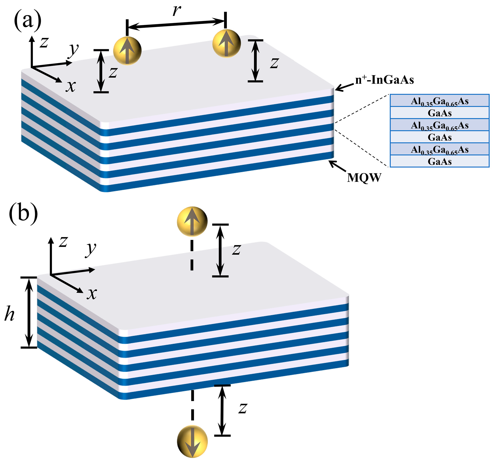
The HMM considered in this work is alternately stacked with degenerately doped InGaAs and an MQW slab which behaves as an active dielectric layer, as shown in
Figure 1. Such a structure can be fabricated by the use of molecular-beam epitaxy with growth on lattice-matched InP substrates [
42]. InGaAs has plasmonic resonances in the mid-infrared (IR) regime, so it can substitute metal (or graphene) in the conventional dielectric–metal (graphene) HMM to form a new type of semiconductor HMM. The permittivity of InGaAs can be described by the Drude-like model:
, where
is the background dielectric value,
is the electron-scattering rate, and
is the plasma frequency. It is easily observed that the real part of permittivity,
is negative when the frequency is less than the plasma frequency. Here, we set the plasma frequency to
, which is the same as that used in Ref. [
36]. Therefore, InGaAs can support SPPs in mid-IR regions, similar to metal that can support SPPs in visible ranges. The MQW is composed of alternating subwavelength layers of Al
0.35Ga
0.65As (AlGaAs) acting as potential barriers and GaAs acting as potential wells, since the band gap of AlGaAs is larger than that of GaAs. The MQW behaves as a uniaxial anisotropic material, and its permittivity can be calculated by use of effective medium theory (EMT). The permittivity of the MQW slab parallel to the interface between components can be expressed as in [
43,
44]:
The permittivity in the direction perpendicular to the MQW interface is given by a Lorentz oscillator model [
43,
44]:
Here,
and
represent the average effective background permittivity. They are expressed as
and
, respectively.
and
denote the undoped background dielectric constants for the potential barrier and well, respectively.
is the plasma frequency of the MQW, with
being the elementary charge of the electron.
is the dielectric constant in vacuum,
is the effective mass of the electron, with
being the mass of the free electron, and
is the electron density per quantum well.
is the oscillator strength of the resonance, which is determined by the ISBT transition energy.
is the electron-scattering rate. When the frequency is larger than the plasma frequency of the MQW, the MQW slab behaves as a pure anisotropic dielectric. The one-dimensional periodic structure, composed of the stacked subwavelength MQW and InGaAs, can be treated as a homogenous anisotropic uniaxial material. According to EMT, the dispersion relation for the entire multilayer InGaAs/MQW can be expressed as
where
and
are the permittivities parallel and perpendicular to the interface, which are, respectively, expressed as in [
44]:
where
and
are given by Equations (1) and (2).
is the filling fraction of InGaAs, where
and
are the thicknesses of InGaAs and the MQW, respectively. From Equations (3)–(5), we can see that the dispersion relation will be hyperbolic when the product of
is less than zero. This means that the entire multilayer MQW/InGaAs plays the role of an HMM. Here, we should mention that EMT, in describing the effective permittivities, is only valid when the thicknesses of the HMM components are much less than the transition wavelength of QEs.
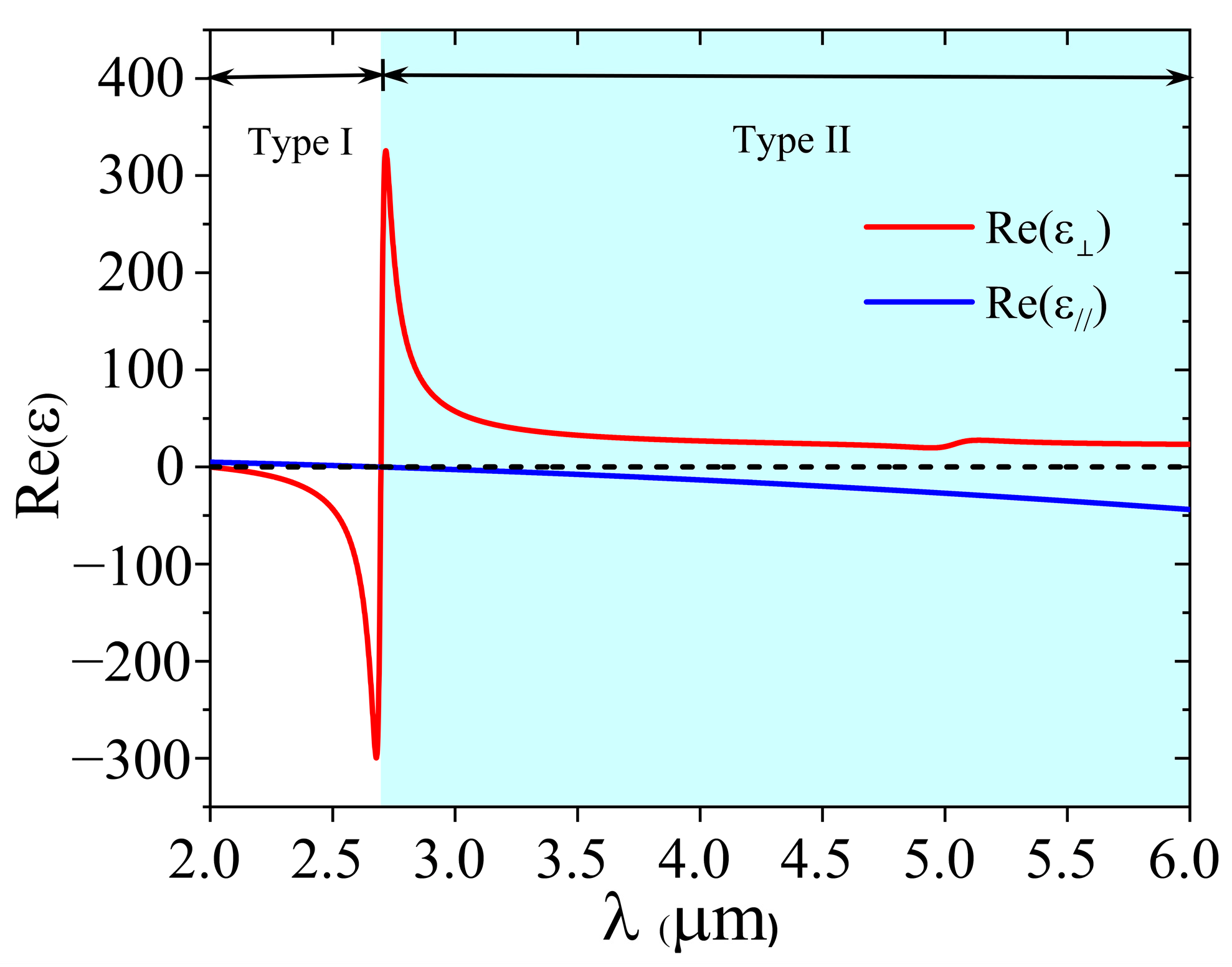
We show the vertical and parallel permittivities of the semiconductor HMM in
Figure 2. We can see that the vertical permittivity is negative, while the parallel permittivity is positive when the wavelength is less than
. This corresponds to the hyperbolic region of type I. When the wavelength is larger than
, the vertical permittivity changes to a positive value abruptly and the parallel permittivity becomes negative; this is the type II hyperbolic region. The wavelength
, corresponding to the optical topological transition (OTT) from type I to type II of the HMM, is called the topological transition wavelength,
[
45]. Interestingly, there is a Lorentzian shape in the vertical permittivity at
, which is caused by the intersubband transitions (ISBTs) in the plane normal to the interface (
z-direction) of the MQWs. In studying the spontaneous emission of two identical QEs near the HMM, we consider two different configurations. In configuration I, two identical QEs are placed at the same side of the HMM at the same distance
, as shown in
Figure 1a. The separation between two QEs is represented by
. For configuration II, two QEs are placed at a different side of the HMM, with both distances being
, as shown in
Figure 1b. Before studying the collective spontaneous emission of two QEs, we first consider the spontaneous emission of a single QE placed near the HMM with a distance
, whose spontaneous emission decay rate can be written as in [
17]:
where
is Planck’s constant.
is the wave vector in free space,
is the electric dipole of the QE, and
is the unit vector along the direction of the dipole moment.
is the Green’s tensor of the system, which is closely related to the reflection coefficient of the HMM. Under the condition of the electric dipole and weak coupling approximations, the normalized spontaneous emission decay rate, also called the Purcell factor, can be expressed as in [
46,
47]:
where
is the spontaneous emission decay rate in vacuum,
is the wave vector component parallel to the
xy plane, and
is the wave vector component along the
direction in free space.
is the
p-polarized reflection coefficient of electromagnetic waves from the surfaces of the HMM, which can be calculated by use of EMT. Considering two identical QEs placed near the HMM, the collective spontaneous emission decay rate of two QEs is defined as in [
17]:
where
is the spontaneous emission decay rate of the QE
at the position
from the contribution of the QE
at the position
, which is expressed as follows:
The exact expressions of normalized
in the reflection configuration and transmission configuration can, respectively, be written as follows [
17]:
and
Here, and is the p-polarized transmission coefficient of the semiconductor HMM, with a thickness of . is the zero-order Bessel function of the first kind. The collective spontaneous emission of two QEs in the proximity of HMM is determined by the decay rate in Equation (8). When the decay rate is larger than 1.0 (), the collective spontaneous emission is enhanced compared with the emission of one individual QE, and the system is in the superradiant state. When the decay rate is less than 1.0 (), the collective spontaneous emission of two QEs is inhibited, indicating that the system is in the subradiant state.
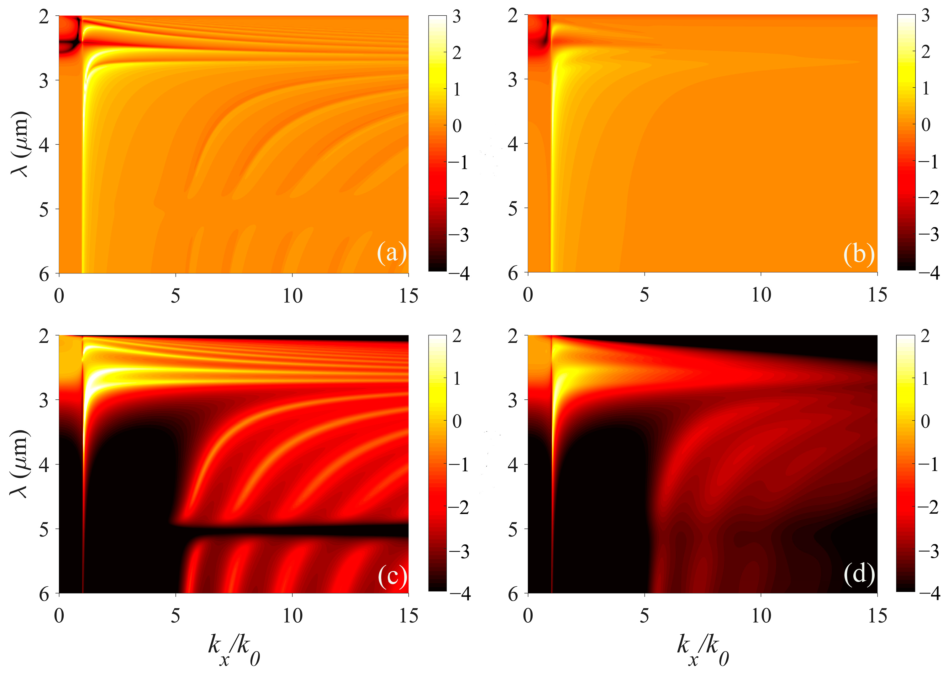
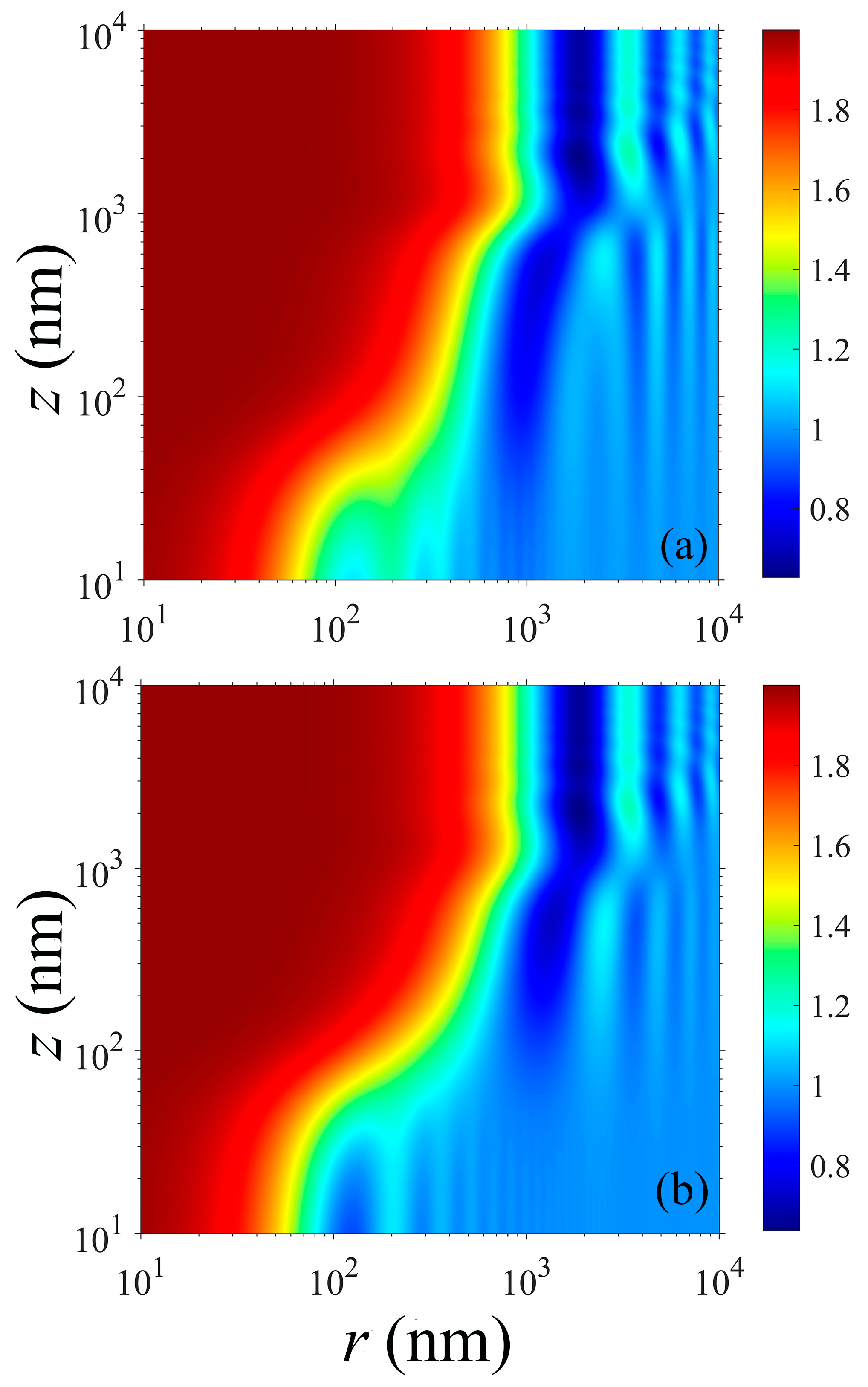
From Equations (7), (10) and (11), we can see that the reflection and transmission coefficients must be obtained before further calculating the spontaneous emission decay rate. Then, we show the imaginary parts of the reflection and transmission coefficients of the semiconductor HMM by considering the situations with and without strong coupling. Here, there are five InGaAs and five MQW layers, and the thicknesses of the InGaAs and MQW are both 80 nm, so the thickness of the total HMM is
nm. When strong coupling is present, the electron-scattering rates for the MQW slab and the InGaAs are set to
and
, respectively.
Figure 3a,c, respectively, show the imaginary parts of the reflection and the transmission coefficients of the HMM with strong coupling. We can see that there are several bright branches arising from the contribution of the hyperbolic modes supported by the InGaAs/MQW structure. In particular, there is a dark band near
, which is caused by the strong coupling between ISBTs and the high-
k mode of the system.
Figure 3b,d, respectively, show the reflection and transmission coefficients of the HMM without strong coupling. The electron-scattering rate in such a system is set to
for the MQW and
for the InGaAs layers, which are the same values as those used in Ref. [
36]. From
Figure 3b,d, we can clearly see that there is no strong coupling in this situation.
3. Spontaneous Emission of Two QEs near HMM in Reflection Configuration
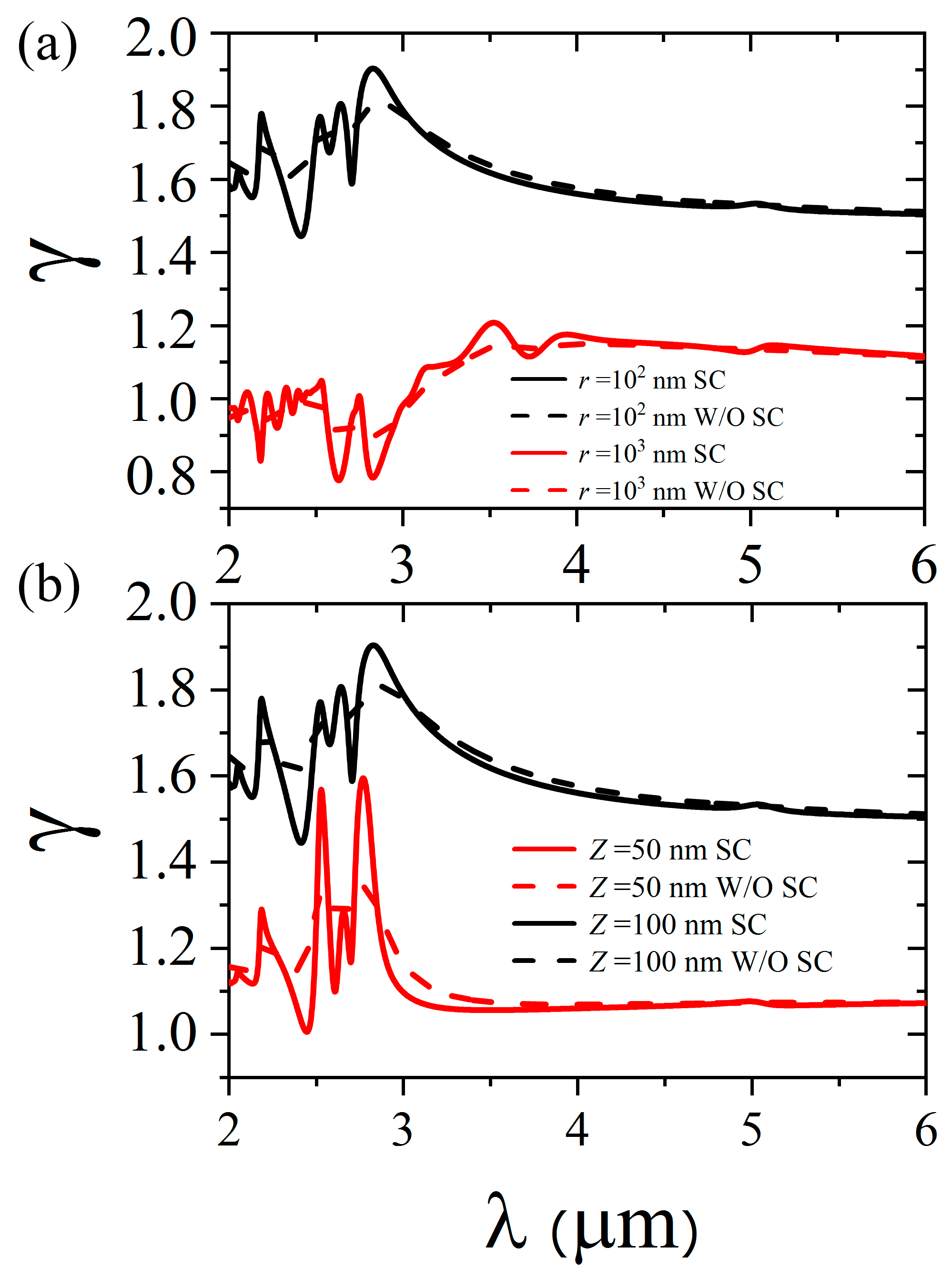
First, we study the collective spontaneous emission of two QEs near the HMM in the reflection configuration, as shown in
Figure 1a. The PbSe or HgTe quantum dots can be used as the QEs since their transition wavelengths can match our considered wavelength range (2 μm to 6 μm). In
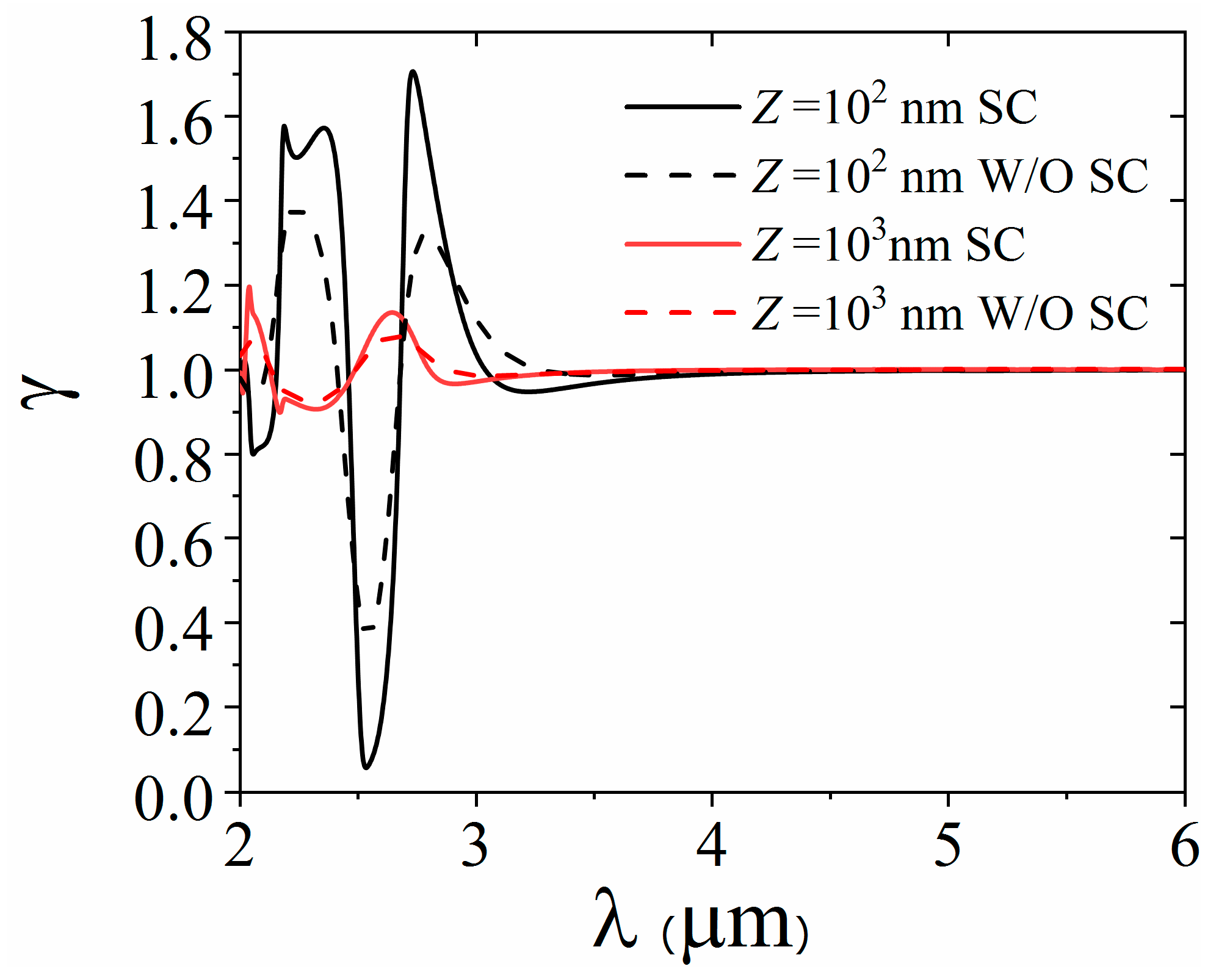
Figure 4a, we show the dependence of the decay rate
factor on the transition wavelength of the QE for a different separation,
. The distances for the two QEs are both fixed at
. The solid and dashed lines denote the situations with and without strong coupling, respectively. We can see that the
factor strongly depends on both the transition wavelength and the coupling state of the HMM. The decay rate varies intensively with the transition wavelength in the type I hyperbolic region, while it changes gently with the transition wavelength in the type II hyperbolic region. The decay rate is larger for the case with a separation value of
nm compared to that with a separation value of
nm. The QEs are in the superradiant state for the separation value of
nm, while the decay rate oscillates between superradiant and subradiant states for the separation value of
nm. When there is no strong coupling, the decay rate changes slowly with the wavelength in the type II hyperbolic region. These phenomena mean that the strong coupling has a significant impact on the collective spontaneous emission of two QEs near the semiconductor HMM. In
Figure 4b, we show the dependence of the
factor on the transition wavelength for a different distance
; the separation between two QEs is fixed at
. It can be seen from
Figure 4b that the decay factor of QEs with a transition wavelength near 2.8 μm still changes intensively when the distance between QEs and the HMM decreases to 50 nm. Therefore, no matter what the separation
and distance
are, strong coupling has a greater effect on the collective spontaneous emission of two QEs compared to the situation without strong coupling. Here, we briefly analyze the physical mechanism of strong coupling on the collective spontaneous emission. In the near-field region, the radiation from the QEs can lead to the excitation of the HPPs in the semiconductor HMM, which predominantly contributes to the spontaneous emission. Meanwhile, the MQW slab shows free-electron movement in the
xy plane and quantum confinement with possible ISBTs in the plane normal to the interfaces. Under special conditions, strong coupling occurs between high-
k HPPs and the ISBTs; the radiation from spontaneous emission will be absorbed by the electrons in the process of ISBTs. Therefore, the collective spontaneous emission will be varied when strong coupling is present.
In order to see the collective spontaneous emission of two QEs near the HMM clearly, we once again show the effect of separation
and distance
on the decay rate
of two QEs in
Figure 5. Here, the transition wavelengths of both QEs are fixed at
. The situations with and without strong couplings are shown in
Figure 5a,b, respectively. We can see in
Figure 5a that the system is in the superradiant state when separation
ranges from
nm to
nm for the considered distance
. This means that the collective spontaneous emission of two QEs is enhanced. In particular, when the distance
ranges from
to
nm, the collective spontaneous emission of QEs can oscillate between the superradiant and subradiant states when the separation
is larger than
nm.
Figure 5b shows the
factor of two QEs in the case without strong coupling. Similarly, the superradiance occurs for the separation
from 10 nm to 80 nm. In this separation region, two QEs keep strong interaction whatever the distance is. But when the separation between QEs is larger than
μm, the
factor oscillates near 1.0 as the separation increases, which shows that the system varies between superradiance and subradiance. Because the separation
of the QEs that realizes superradiance in a strongly coupled system is different from the separation
in the case of no strong coupling, the interaction between the QEs can be adjusted by regulating the state of the material.
4. Spontaneous Emission of Two QEs near Semiconductor HMM in Transmission Configuration
Here, we continue to study the collective spontaneous emission of two QEs near the HMM in the transmission configuration with the schematic shown in
Figure 1b. In
Figure 6, we display the dependence of the decay rate
on the transition wavelength by considering the presence and absence of strong coupling. The distance between each QE and the semiconductor HMM is set to
nm, as shown in black lines. We can see that the decay rate varies quickly between the superradiant state and subradiant state as the transition wavelength increases from 2.0 to 3.0 μm. Then, the decay rate almost stays at 1.0 when the transition wavelength is larger than 3.0 μm. Meanwhile, the change of the decay rate under strong coupling is larger than that without strong coupling. The decay rate of the system with a distance of 1000 nm is also shown in red lines for comparison. It can be clearly seen that the collective spontaneous emission becomes weak when the distance becomes larger. Similarly, strong coupling still has a larger effect on the collective spontaneous emission compared to when there is no strong coupling, even when the distance is large. These phenomena indicate that strong coupling has an important influence on the
factor of the system in the case of transmission configuration.
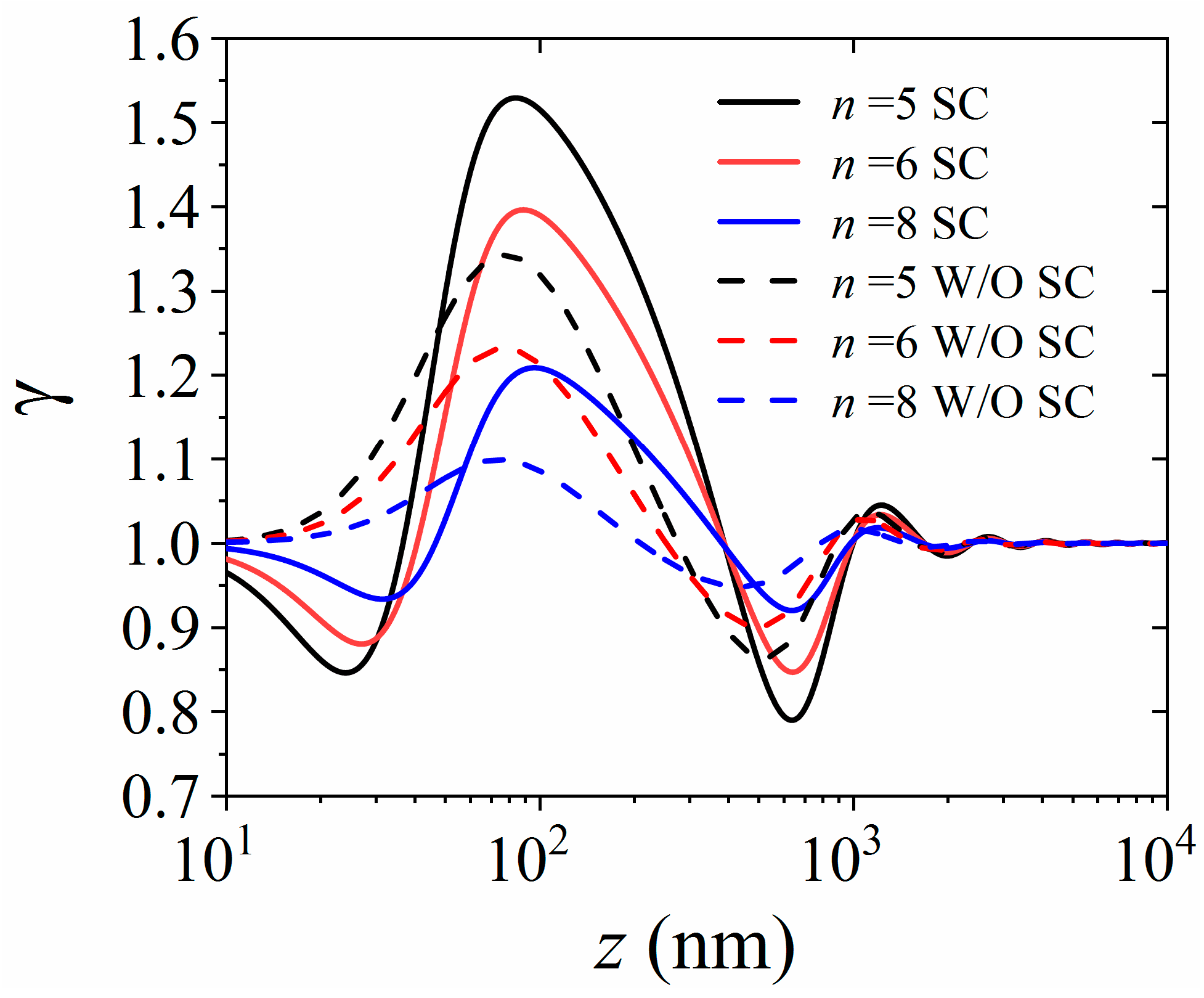
Here, in
Figure 7, we continue to study the dependence of the collective spontaneous emission of two QEs on the distance
for a different number of layers of the HMM. The situations with and without strong coupling are displayed in solid and dashed lines, respectively. When there is strong coupling in the HMM, the decay rate first decreases and then increases when the distance ranges from 10 nm to 100 nm. The decay rate can reach the maximum value when the distance is about 100 nm, while it decreases rapidly as the distance continues to increase. The decay rate exhibits oscillations near 1.0 when the distance is larger than 1000 nm, indicating the interaction between two QEs becomes weak when the distance is large enough. However, for the system without strong coupling, the decay rate first increases as the distance increases from 10 nm to 100 nm, which is different from the situation with strong coupling. The decay rate can also reach the maximum value when the distance is near 100 nm. We can see that the maximum decay rate for the situation without strong coupling is less than that for the situation with strong coupling. In addition, the number of layers also has an important effect on the maximum decay rate, which decreases as the number of layers increases. This is because as the thickness of the total structure increases, the two QEs are farther apart, but the HPPs contribute to spontaneous emission only in the near-field region.
Finally, we qualitatively analyze the effects of some other environmental factors on the collective spontaneous emission of two QEs. Because the strong coupling, which predominantly contributes to the collective spontaneous emission, is from the high-
k HPPs and the ISBTs, the environmental factors, such as the imperfections in HMMs, will disturb the ISBTs and then the strong coupling. In this situation, the strong coupling may disappear, so the imperfections may disadvantage the collective spontaneous emission. In addition, the experimental observation of the collective spontaneous emission may be possible due to the development of nanofabrications. The semiconductor HMM can be fabricated by molecular-beam epitaxy with growth on lattice-matched InP substrates [
42]. The PbSe or HgTe quantum dots can be used as the QEs. The experimental method provided in Ref. [
38] can be employed, where the authors observed that the spontaneous emission rate of rhodamine dye molecules can be enhanced 76-fold by using nanopatterned multilayer HMMs.
