Article

On-Chip Photonic Convolutional Processing Lights Up Fourier Neural Operator

1
College of Computer Science and Technology, National University of Defense Technology, Changsha 410073, China
2
Institute for Quantum Science and Technology, College of Science, National University of Defense Technology, Changsha 410073, China
3
National Innovation Institute of Defense Technology, Academy of Military Sciences PLA China, Beijing 100071, China
*
Authors to whom correspondence should be addressed.
Photonics 2025, 12(3), 253; https://doi.org/10.3390/photonics12030253
Submission received: 4 February 2025 / Revised: 5 March 2025 / Accepted: 10 March 2025 / Published: 12 March 2025
(This article belongs to the Special Issue The Principle and Application of Photonic Metasurfaces)

Abstract

:
Fourier Neural Operators (FNOs) have gained increasing attention for their effectiveness in extracting frequencydomain features and efficiently approximating functions, making them wellsuited for classification tasks. However, the absence of specialized photonic hardware has limited the acceleration of FNO inference. In this study, we introduce what we believe is the first photonic hardware framework dedicated to speeding up the Fourier layer of an FNO. Our approach employs a frequency domain convolutional photonic chip and a micro-ring array chip, achieving 5-bit quantization precision in the inference process. On the Radio ML 2016.10b dataset, our Fourier convolutional neural network achieves a peak identification accuracy of 95.50%, outperforming standard convolution-based networks. These findings highlight the transformative potential of co-designing software and hardware, demonstrating how photonic computing can deliver specialized acceleration for critical AI components and substantially improve inference efficiency. Ultimately, this work lays a foundation for integrating photonic technologies into next-generation AI accelerators, pointing to a promising direction for further research and development in optoelectronic hybrid computing.

1. Introduction

The Fourier Neural Operator (FNO) has received considerable interest lately because of its remarkable ability to efficiently approximate functions and extract features in the frequency domain [1]. This unique capability has enabled FNOs to excel in various applications, including image classification and the numerical solution of systems of partial differential equations (PDEs) [2]. By leveraging Fourier transforms, FNO can capture complex patterns and relationships within data, thereby establishing itself as a formidable resource in both machine learning and computational mathematics [3,4].
However, existing software-based implementations of FNOs have yet to fully realize their potential, primarily constrained by the lack of hardware accelerators specifically designed for their unique operational characteristics. Current FNO architectures largely rely on traditional computing frameworks, which fail to capitalize on the advantages of frequency domain processing, leading to inefficiencies in speed and energy consumption [5]. Against the backdrop of increasing demands for real-time processing and large-scale data analysis, the development of dedicated hardware to accelerate FNO computations becomes critically important. In this context, optical computing offers a promising approach to improve the performance of FNOs, as optical systems provide unparalleled advantages, including high-speed processing, massive parallelism, and significantly reduced power consumption [6,7,8,9,10,11,12]. In recent years, researchers have begun to explore the potential of optical devices in efficiently implementing neural network architectures, particularly with notable advancements in the realization of optical FFT [13,14,15,16]. The Fast Fourier Transform (FFT) is a critical component of FNO, directly influencing its performance and efficiency [1]. Photon implementation of the CooleyTukey algorithm, for instance, demonstrates exceptional performance in sub-nanosecond signal processing applications, laying a foundational path for diverse optical Fourier transform implementations [13].
Traditional optical FFT implementations rely on cascaded forward and inverse transform modules, which not only introduce additional insertion loss but also increase the chip’s footprint [13,14,17]. To address this issue, our work innovatively circumvents the explicit FFT module by achieving time-domain multiplication (functionally equivalent to frequency domain convolution), while maintaining a quantization precision of 5 bits. As the first hybrid optoelectronic realization of this paradigm, we successfully integrated a frequency domain convolution photonic chip (realizing the Fourier integral operator) and a micro-ring resonator (MRR) array chip (performing linear transformation) within a unified optical framework. This end-to-end photonic mapping mechanism seamlessly aligns with the mathematical formulation of FNO, significantly enhancing system performance. Experimental validation on the Radio ML 2016.10b dataset [18] demonstrates that the proposed photonic Fourier layer implementation of the Fourier convolutional neural network (FCNN) achieves a peak recognition accuracy of 95.50%. This synergistic optimization of hardware and algorithms overcomes the latency and efficiency limitations of software models, thereby providing a solid foundation for building scalable photonic learning systems. The optoelectronic hybrid computing framework presented herein opens new avenues for realizing high-speed, low-power artificial intelligence processing architectures.

2. Methods

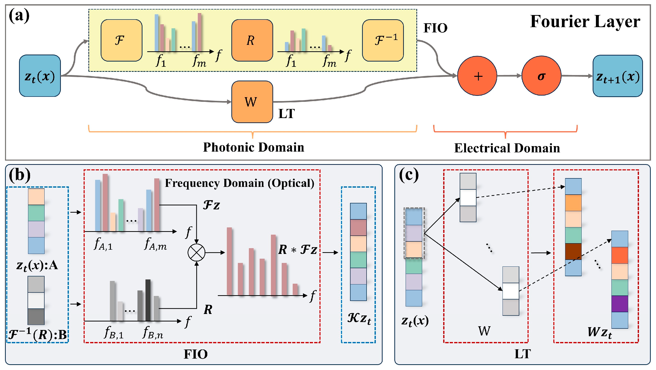
2.1. Principles of Implementing Fourier Layer with Photonic Computing Hardware

As illustrated in Figure 1a, the Fourier layer (FL) receives the input z t x , which is subsequently divided into two branches. The upper branch applies a Fourier transform, denoted as , followed by a linear transformation R that acts on the low-frequency modes in the Fourier space. The transformed data are then processed using the inverse Fourier transform F 1 (this process is abbreviated as Fourier integral operator, FIO). Meanwhile, the lower branch employs a local linear transformation (abbreviated as linear transform, LT). The outputs from these two branches are then summed and passed through a nonlinear activation function. The entire process can be expressed as follows:
z t + 1 x = σ ( W z t x + ( K z t ) ( x ) )
where FIO is ( K z t ) x , which can be further expressed as follows:
( K z t ) x = F 1 ( R F z t ) ( x )
For the implementation of the FIO, we utilize the operational process illustrated in Figure 1b. Initially, the data representing z t x is encoded as A and subsequently modulated onto the optical domain using an electro-optic modulator. The frequency domain representation of this signal is denoted as F z t . Simultaneously, the data corresponding to F 1 R are encoded as B and modulated onto the optical domain via an electro-optic modulator, resulting in the frequency domain representation R. The two signals are then multiplied together. According to the convolution theorem, the multiplication in the time domain corresponds to convolution in the frequency domain, which can be expressed as R F z t . Consequently, the resulting time-domain data can be represented as F 1 ( R F z t ) ( x ) . This process highlights the efficiency of using optical modulation techniques to perform complex operations such as the FIO, thereby enhancing the computational capabilities of photonic neural networks.
For the implementation of the LT, we consider the convolution between the vector z t x and the convolutional kernel W , as illustrated in Figure 1c. To address challenges related to hardware scalability, particularly when processing long vectors, we employ a strategy that decomposes the original long vector operations into shorter vector operations compatible with the hardware scale. This approach simulates the sliding window operation in the convolution process. Furthermore, the dashed box enclosing indicates the capability to compute multiple convolutional kernels simultaneously with the input data within the sliding window, ultimately yielding multiple convolved feature datasets. This method not only enhances computational efficiency but also ensures compatibility with the constraints of photonic hardware, thereby facilitating scalable and efficient implementations.
Finally, the computation outputs from the FIO and LT modules undergo optical-to-electrical conversion, followed by summation and nonlinear activation in the back-end digital computing (e.g., computer), ultimately yielding the final output z t + 1 x .

2.2. Principles of Photonic Computing Chips

To validate principles of the FIO and LT noted in the previous section, we developed photonic convolution circuits specifically for one-dimensional (1D) data. As shown in Figure 2a, a laser source at wavelength λ c is vertically coupled into the photonic chip via a grating coupler and then split into two beams by an on-chip beam splitter. These beams are subsequently directed into two IQ modulators (IQ Mod SI and IQ Mod LO), indicated by red dashed boxes in the figure. The input signal z t ( x ) is generated using an arbitrary waveform generator (AWG), then amplified by a radio frequency (RF) driver and routed into IQ Mod SI, where it is loaded into the optical domain. Meanwhile, the time-domain data corresponding to the convolution kernel F 1 ( R ) are also generated by the AWG, amplified, and fed into IQ Mod LO for optical modulation. The two beams are then combined at a 90° hybrid, and the resulting signal is processed by a balanced photodetector (BPD) to yield the frequency domain convolution R F z t ( x ) . The time domain of this result is F 1 ( R F z t ( x ) ) , which is the desired output. Further details on the derivation can be found in Section S1 of the Supplementary Materials.
For the LT implementation, we investigated a 1D convolution where the kernel size is 3. As displayed in Figure 2b, we propose a 3 × 3 MRR array chip to perform this convolution. To avoid interference among resonance peaks, we designed MRRs with diameters of 14 µm, 22 µm, and 30 µm, respectively. Three non-overlapping resonance peaks were identified as the operating wavelengths, denoted as λ A , λ B , and λ C . For each column of MRR array, a sliding window of the input data, [ x 1 , x 2 , x 3 ] , is supplied, and the output from the photodetector (PD) represents a weighted sum:
y 1 y 2 y 3 = P D 3 P D 2 P D 1 = w A 11 x A 1 + w B 12 x B 2 + w C 13 x C 3 w C 21 x C 1 + w A 22 x A 2 + w B 23 x B 3 w B 31 x B 1 + w C 32 x C 2 + w A 33 x A 3 = w 11 x 1 + w 12 x 2 + w 13 x 3 w 21 x 1 + w 22 x 2 + w 23 x 3 w 31 x 1 + w 32 x 2 + w 33 x 3
That is, y i = j = 1 3 w i j x j . By treating the three elements in each sliding window as the convolution input and the transmission of three MRRs in each column as the elements of convolutional kernel w i j , the output of each column corresponds to one convolution result y i . Multiple columns can thus implement different kernels on the same input window in parallel. Consequently, this 3 × 3 MRR array can simultaneously carry out convolution-based linear transformations, offering a practical approach for small-scale neural network operations on photonic chips.

3. Results

After designing the photonic circuits for FIO and LT, we conducted experimental measurements to evaluate their effectiveness in practical operation.

3.1. Experimental Evaluation of FIO Quantization Precision

Figure 3a illustrates the experimental setup for testing the quantization bit depth of FIO. The light source is provided by an external laser with power of 13 dBm, which is amplified by an Erbium-Doped Fiber Amplifier (EDFA). A polarization controller is used to adjust the polarization state, ensuring maximum power coupling vertically into the frequency domain convolution chip. The signals z t ( x ) and R involved in the computation are encoded as radio frequency signals by an arbitrary waveform generator. These signals are then amplified by a radio frequency driver amplifier and connected to the on-chip IQ modulator for electro-optic conversion. The output from the chip is amplified by a Transimpedance Amplifier (TIA) before being input into an oscilloscope, which performs a Fast Fourier Transform (FFT) to obtain the computation results.
First, as shown in Figure 3b, we measured the key performance metrics of the modulator, which play a critical role in implementing the FIO. The results indicate that the 3 dB bandwidth of the modulator is approximately 23 GHz, demonstrating that convolution operations can be performed over a wide range of modulation frequencies to meet diverse computational requirements. Next, to assess the achievable accuracy of frequency domain convolution, we selected two vectors, A = [ 1,1 , , 1 ] 64 and B = [ 1,1 , , 1 ] 64 , for computation. The elements of these vectors were encoded into the radio frequency signals S and L through an AWG. The frequency distribution for signal S was [80, 160, 240, …, 5040, 5120] MHz, while that for signal L was [60, 140, 220, …, 5020, 5100] MHz. Based on the photonic circuit illustrated in Figure 2a and the corresponding experimental parameters, we acquired time-domain signals at the output using the oscilloscope. We then processed the captured data with FFT algorithm, and the comparison results are presented in Figure 3c. It is evident that the experimental results deviate from the theoretical values, primarily due to system noise (e.g., device noise and electrical noise). The histogram in Figure 3c also shows that, when using the standard deviation of the error as 0.0206, the precision of computation is approximately 5 bits.

3.2. Experimental Evaluation of LT Quantization Precision

Figure 4a illustrates the experimental setup for testing the quantization precision of the LT, which implements a 1D convolutional operation. In the Data Loading stage, the vector to be processed is intensity-modulated by nine modulators and loaded onto light generated by three lasers with different wavelengths (λA, λB, and λC). The modulated signals are first combined using an off-chip wavelength-division multiplexer (WDM) based on beam combiners, generating multi-wavelength optical signals for each row (e.g., x A 1 + x B 1 + x C 1 , where x A 1 indicates that the vector element x 1 is loaded onto wavelength λA). Finally, they are vertically coupled into the photonic chip via a grating coupler with an insertion loss of 3 dB. A polarization controller optimizes the transverse-electric (TE) mode alignment to minimize polarization-dependent losses. Within the chip, the MRR array performs the weighted summation, and the output signals are detected by three PDs. For clarity, the multi-channel power supply controlling the MRR weights is omitted in this schematic.
In the Photonic Computing stage, MRR chips are fabricated on a standard 220 nm SOI platform. The MRR array chip occupies an area of about 1.2 × 1.2 mm2 and is fabricated using a 180 nm node process, ensuring significant integration density. Figure 4b presents the spectral responses of MRRs with diameters of 14 μm, 22 μm, and 30 μm, corresponding to FSRs of 12.51 nm, 8.13 nm, and 6.08 nm, respectively. Each MRR exhibits an extinction ratio exceeding 27 dB, meeting the precision requirements for our calculations. Building upon these findings, the following experiments are conducted to further explore the effectiveness of the MRR array in one-dimensional (1D) convolutions. First, the operational wavelengths of the MRR array are determined from the measured spectral responses, ensuring that each MRR is appropriately assigned to a distinct resonance peak. That is, the operating wavelengths of 1540.105 nm (λA), 1554.440 nm (λB), and 1548.970 nm (λC) are chosen, corresponding to the resonance wavelengths of MRRs with diameters of 14, 22, and 30 μm, respectively. Next, 500 random pairs consisting of 1 × 3 weight matrices and corresponding 3 × 1 input vectors are generated, and their expected outputs are calculated in advance. The weight matrices are then loaded onto the MRR array through a multi-channel power supply, while the input vectors are modulated onto the laser source via a modulator array. The output of each MRR column is collected by a PD and normalized for comparison with theoretical values, as shown in Figure 4c. The experimental results show a strong correlation with theoretical values (Pearson’s r = 0.99). Additionally, the errors between the experimental and theoretical values are statistically analyzed and represented as a histogram in the inset, revealing a standard deviation of 0.019, which is smaller than the quantization interval of 0.0323 for 5-bit precision. Therefore, the experimental results demonstrate that the 1D convolution operation performed on this MRR array chip achieves 5-bit precision. Consequently, in subsequent recognition task experiments, a 5-bit quantization precision will be adopted to ensure that the bit-width of quantization-aware training aligns with the hardware implementation.

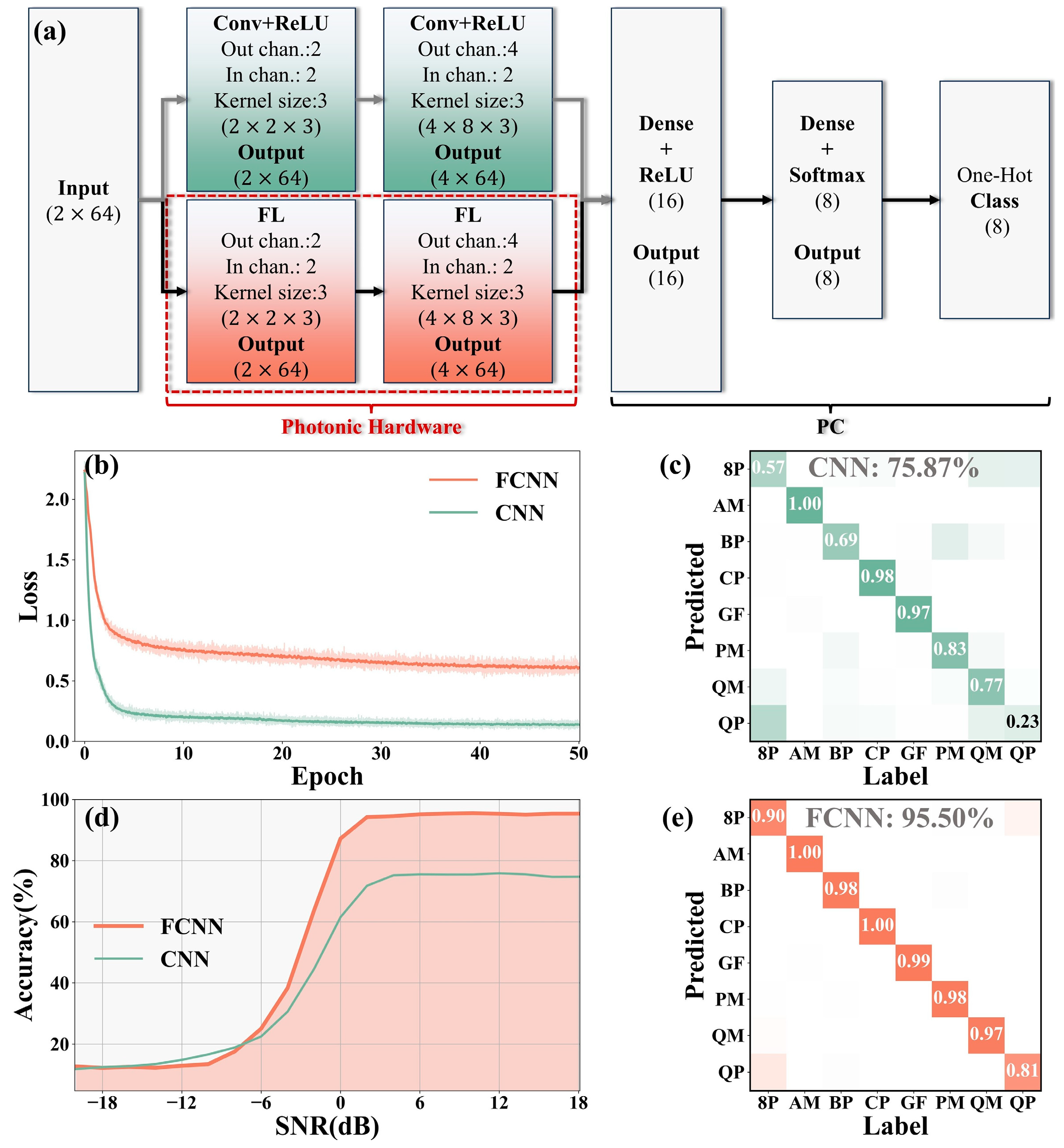
3.3. Fourier Convolutional Neural Network for Classification Tasks

To evaluate the performance of the FL photon accelerator in FNO in practical applications, we conducted an eight-class classification task on the Radio ML 2016.10b dataset (our targeted task does not include QAM16 and WBFM). We designed two models for comparison: a Fourier convolutional neural network (FCNN), which uses the proposed photonic accelerator for its FL, and a standard one-dimensional convolutional neural network (CNN). As shown in Figure 5a, each model has six layers in total: an input layer, two feature extraction layers, and three fully connected layers (with the final layer serving as the output layer). In the FCNN, the input layer—sized 2 × 64—represents the IQ components of the signal, followed by two FLs implemented in photonic hardware for feature extraction, and three fully connected layers that handle feature integration and classification. The last fully connected layer contains eight neurons, corresponding to eight categories of modulation. In contrast, in the CNN, the two feature extraction layers are replaced with one-dimensional convolutional layers. All network layers use the ReLU activation function for nonlinear activation.
We implemented both models in PyTorch 2.2.2. Since FLs of the FCNN use photonic hardware during inference, we applied quantization-aware training of 5-bit to those layers to mimic hardware precision; the three fully connected layers run on a standard computer in single-precision floating-point. We used the cross-entropy loss function with the Adam optimizer (learning rate = 0.001) and trained for 30 epochs, after which we saved the final models and training details. Figure 5b shows that the FCNN converged after about 10 epochs, while the CNN took around 25 epochs. This faster convergence for the FCNN is also supported by the loss curves, indicating better recognition performance. Once training was complete, we tested the models. During inference, the feature extraction portion of the FCNN was carried out on photonic hardware, whereas the CNN runs entirely on a conventional PC. Figure 5d summarizes the recognition accuracy across various signal-to-noise ratios (SNRs). The FCNN and CNN attained overall recognition accuracies of 58.21% and 46.73%, respectively. At SNR = 10, the FCNN achieves a peak accuracy of 95.50%, whereas the CNN reaches only 75.87% at SNR = 12. We further examined the confusion matrices under each model’s best accuracy, shown in Figure 5c,e. These results confirm that the FCNN outperforms the CNN in both overall and peak accuracy, highlighting the efficacy of photonic FLs for this task.

4. Discussion

This study addresses the current limitation of existing FNO implementations, which lack specialized photonic hardware. Based on the design philosophy of optoelectronic hybrid computing, we successfully integrated a frequency domain convolution photonic chip and an MRR array chip into the FL of an FNO, thereby realizing both the FIO and LT. This achievement marks an important step in the fusion of photonic computing and deep neural network architectures. The specialized photonic accelerator can perform computations of FL with 5-bit quantization precision. When applied to the Radio ML 2016.10b dataset under optimal SNR conditions, the proposed FCNN achieved an accuracy of 95.50%, significantly surpassing the 75.87% accuracy of traditional CNNs, demonstrating how photonic computing can effectively enhance the performance of specialized deep learning models. However, it is important to note that this frequency domain convolution method is not suitable for general Fast Fourier Transform (FFT) computations, as its inputs and outputs are in the time domain rather than the frequency domain. This method is not a direct substitute for general optical FFT processors but is better suited for deployment in architectures like photonic neural networks, which have explicit frequency domain operations while using time-domain input and output formats.
To demonstrate the advantages of our system, as shown in Table 1, we compared it with Ref. [17] (explicit FFT/IFFT modules cascaded with optical kernels) and the photonic tensor core for matrix multiplication [8]. The computation of the performance indicators can be found in Section S2 of the Supplementary Materials [19]. Table 1 shows that our FIO module achieves a theoretical peak computing power of 5.54 TOPS (tera Ops per second), surpassing the 0.11 TOPS of Ref. [17], by implementing frequency domain convolution through direct time-domain optical signal multiplication (based on Fourier convolution theorem equivalence). This approach eliminates losses from explicit FFT/IFFT modules and allows flexible kernel configuration without hardware reconfiguration. Despite the constraints imposed by the RF power requirements of IQ modulators, our system achieves an energy efficiency of 6.92 TOPS/W, slightly higher than the 6.29 TOPS/W reported in Ref. [17]. However, the larger footprint of IQ modulators results in a lower integration density compared to compact diffractive couplers or Mach–Zehnder interferometer (MZI)-based designs [13,14]. When compared to Refs. [15,16], although the general FFT functionality is sacrificed, our approach offers a more efficient implementation pathway for specific convolution tasks, demonstrating significant potential for application in optical computing.
As a proof of concept, this work presents significant optimization opportunities in three areas: chip, architecture, and application. First, at the chip level, some functions still rely on external devices (such as off-chip WDMs). Therefore, optimizing the design of on-chip devices (for example, more compact IQ modulators with lower half-wave voltages to reduce radio frequency power) and exploring diverse MRR arrays and convolution chip configurations will further enhance the overall performance of the chip. Second, at the architecture level, this study primarily focuses on implementing optical FIOs and LTs in the optical domain. However, the integration of information from these two modules still depends on optoelectronic hybrid processing. Future work will emphasize exploring the implementation of all-optical summation and nonlinear activation [20] while balancing the computational power gap between FIO and LT to ensure the entire system can operate at maximum computational capacity. This progress will lay the foundation for a fully integrated optical Fourier layer, ultimately achieving a complete optical Fourier convolutional neural network. Finally, at the application level, due to current limitations in quantization precision, this study has only demonstrated classification tasks. Therefore, subsequent work will explore the use of optical FLs to solve PDEs, a common application of FNOs, which will showcase broader adaptability and robustness. Overall, this research paves the way for future innovations in optical computing and neural networks, creating new possibilities for developing efficient and powerful artificial intelligence systems to tackle complex real-world challenges.

Supplementary Materials

The following supporting information can be downloaded at https://www.mdpi.com/article/10.3390/photonics12030253/s1.

Author Contributions

Conceptualization, Z.T. and J.Z.; methodology, H.O.; writing—original draft preparation, Z.T.; writing—review and editing, H.O. and S.D.; visualization, H.O. and Q.Y.; supervision, J.Y. and J.Z.; funding acquisition, J.Y. and H.H. All authors have read and agreed to the published version of the manuscript.

Funding

This research was funded by the National Natural Science Foundation of China (11902358, 62302504).

Institutional Review Board Statement

Not applicable.

Informed Consent Statement

Not applicable.

Data Availability Statement

Dataset available on request from the authors.

Conflicts of Interest

The authors declare no conflicts of interest.

References

  1. Li, Z.; Kovachki, N.; Azizzadenesheli, K.; Liu, B.; Bhattacharya, K.; Stuart, A.; Anandkumar, A. Fourier Neural Operator for Parametric Partial Differential Equations. arXiv 2020, arXiv:2010.08895. [Google Scholar]
  2. Cheng, Y.; Tang, B.; Hub, Z.; Liu, J. Fourier Neural Operator Network for the Signal Generation and Prediction. In Proceedings of the 2024 International Conference on Microwave and Millimeter Wave Technology (ICMMT), Bejing, China, 16 May 2024; pp. 1–3. [Google Scholar]
  3. Johnny, W.; Brigido, H.; Ladeira, M.; Souza, J.C.F. Fourier Neural Operator for Image Classification. In Proceedings of the 2022 17th Iberian Conference on Information Systems and Technologies (CISTI), Madrid, Spain, 22 June 2022; pp. 1–6. [Google Scholar]
  4. Huang, L.-J.; Wang, Y.-M. Fourier Series Neural Networks for Classification. In Proceedings of the 2018 IEEE International Conference on Applied System Invention (ICASI), Chiba, Japan, 13–17 April 2018; pp. 881–884. [Google Scholar]
  5. Hojabr, R.; Sedaghati, A.; Sharifian, A.; Khonsari, A.; Shriraman, A. SPAGHETTI: Streaming Accelerators for Highly Sparse GEMM on FPGAs. In Proceedings of the 2021 IEEE International Symposium on High-Performance Computer Architecture (HPCA), Seoul, Repubic of Korea, 27 February–3 March 2021; pp. 84–96. [Google Scholar]
  6. Zhou, H.; Dong, J.; Cheng, J.; Dong, W.; Huang, C.; Shen, Y.; Zhang, Q.; Gu, M.; Qian, C.; Chen, H.; et al. Photonic Matrix Multiplication Lights up Photonic Accelerator and Beyond. Light Sci. Appl. 2022, 11, 30. [Google Scholar] [CrossRef] [PubMed]
  7. Shen, Y.; Harris, N.C.; Skirlo, S.; Prabhu, M.; Baehr-Jones, T.; Hochberg, M.; Sun, X.; Zhao, S.; Larochelle, H.; Englund, D.; et al. Deep Learning with Coherent Nanophotonic Circuits. Nat. Photon. 2017, 11, 441–446. [Google Scholar] [CrossRef]
  8. Bai, B.; Yang, Q.; Shu, H.; Chang, L.; Yang, F.; Shen, B.; Tao, Z.; Wang, J.; Xu, S.; Xie, W.; et al. Microcomb-Based Integrated Photonic Processing Unit. Nat. Commun. 2023, 14, 66. [Google Scholar] [CrossRef] [PubMed]
  9. Xu, X.; Tan, M.; Corcoran, B.; Wu, J.; Boes, A.; Nguyen, T.G.; Chu, S.T.; Little, B.E.; Hicks, D.G.; Morandotti, R. 11 TOPS Photonic Convolutional Accelerator for Optical Neural Networks. Nature 2021, 589, 44–51. [Google Scholar] [CrossRef] [PubMed]
  10. Xu, Z.; Zhou, T.; Ma, M.; Deng, C.; Dai, Q.; Fang, L. Large-Scale Photonic Chiplet Taichi Empowers 160-TOPS/W Artificial General Intelligence. Science 2024, 384, 202–209. [Google Scholar] [CrossRef] [PubMed]
  11. Cheng, J.; Huang, C.; Zhang, J.; Wu, B.; Zhang, W.; Liu, X.; Zhang, J.; Tang, Y.; Zhou, H.; Zhang, Q.; et al. Multimodal Deep Learning Using On-Chip Diffractive Optics with in Situ Training Capability. Nat. Commun. 2024, 15, 6189. [Google Scholar] [CrossRef] [PubMed]
  12. Ashtiani, F.; Geers, A.J.; Aflatouni, F. An On-Chip Photonic Deep Neural Network for Image Classification. Nature 2022, 606, 501–506. [Google Scholar] [CrossRef] [PubMed]
  13. Ahmed, M.; Al-Hadeethi, Y.; Bakry, A.; Dalir, H.; Sorger, V.J. Integrated Photonic FFT for Photonic Tensor Operations towards Efficient and High-Speed Neural Networks. Nanophotonics 2020, 9, 4097–4108. [Google Scholar] [CrossRef]
  14. Ong, J.R.; Ooi, C.C.; Ang, T.Y.L.; Lim, S.T.; Png, C.E. Photonic Convolutional Neural Networks Using Integrated Diffractive Optics. IEEE J. Select. Top. Quantum Electron. 2020, 26, 1–8. [Google Scholar] [CrossRef]
  15. Li, J.; Fu, S.; Xie, X.; Xiang, M.; Dai, Y.; Yin, F.; Qin, Y. Low-Latency Short-Time Fourier Transform of Microwave Photonics Processing. J. Light. Technol. 2023, 41, 6149–6156. [Google Scholar] [CrossRef]
  16. Di Toma, A.; Brunetti, G.; Armenise, M.N.; Ciminelli, C. LiNbO3-Based Photonic FFT Processor: An Enabling Technology for SAR On-Board Processing. J. Light. Technol. 2025, 43, 912–921. [Google Scholar] [CrossRef]
  17. Zhu, H.H.; Zou, J.; Zhang, H.; Shi, Y.Z.; Luo, S.B.; Wang, N.; Cai, H.; Wan, L.X.; Wang, B.; Jiang, X.D.; et al. Space-Efficient Optical Computing with an Integrated Chip Diffractive Neural Network. Nat. Commun. 2022, 13, 1044. [Google Scholar] [CrossRef] [PubMed]
  18. O’Shea, T.; West, N. Radio Machine Learning Dataset Generation with GNU Radio. Proc. GNU Radio Conf. 2016, 1, 1. [Google Scholar]
  19. Zhang, J.; Tao, Z.; Yan, Q.; Du, S.; Tang, Y.; Liu, H.; Wei, K.; Zhou, T.; Jiang, T. Dual Optical Frequency Comb Neuron: Co-Developing Hardware and Algorithm. Adv. Intell. Syst. 2023, 5, 2200417. [Google Scholar] [CrossRef]
  20. Tao, Z.; You, J.; Ouyang, H.; Yan, Q.; Du, S.; Zhang, J.; Jiang, T. Silicon Photonic Convolution Operator Exploiting On-Chip Nonlinear Activation Function. Opt. Lett. 2025, 50, 582. [Google Scholar] [CrossRef] [PubMed]
Figure 1. Fourier layer. (a) Schemes of Fourier layer [1]. FIO: Fourier integral operator. LT: linear transform. (b) The process of FIO in the proposed architecture. (c) The process of LT in the proposed architecture.
Photonics 12 00253 g001
Figure 2. Schematic of photonic hardware. (a) Schematic diagram for implementing FIO. (b) Schematic diagram for implementing LT. (c) Layout of the frequency domain convolution chip. (d) Layout of the 3 × 3 MRR array chip.
Photonics 12 00253 g002
Figure 3. The measurement setup and results of FIO. (a) The measurement path of FIO. FreqConv Chip: the frequency domain convolutional chip. EDFA: Erbium-Doped Fiber Amplifier. Drivers: RF driver. PC: polarization controller. TIA: Transimpedance Amplifier. (b) The 3 dB bandwidth of the optical modulator. (c) Quantization measurement results of the frequency domain convolutional chip.
Photonics 12 00253 g003
Figure 4. The measurement setup and results of LT. (a) The measurement path of LT. LS: laser. IM: intensity modulator. WDM: wavelength-division multiplexer. PoC: polarization controller. (b) Resonance peaks of MRR array. (c) The quantization precision of the MRR array.
Photonics 12 00253 g004
Figure 5. Demonstration of classification tasks. (a) Neural network based on FL and convolutional layers (Conv). Photonic hardware and PC represent the corresponding parts of the inference process implemented by photonic hardware or a PC, respectively. FL: Fourier layers. (b) Loss function during the training process. (c) Confusion matrix for the Radio ML 2016.10b classification using Conv. (d) Tested accuracy with various SNR. (e) Confusion matrix of Radio ML 2016.10b classification using FNO. 8P: 8PSK, AM: AM-DSB, BP: BPSK, CP: CPFSK, GF: GFSK, PM: PAM4, QM: QAM64, QP: QPSK. Green and orange represent the accuracy of CNN and FCNN, respectively, with deeper colors indicating higher accuracy.
Photonics 12 00253 g005
Table 1. Performance comparison of related works.
Work Peak Computing Power *
(TOPS)
On-chip Efficiency *
(TOPS/W)
Ref. [8]0.1360.20
Ref. [17]0.116.29
Our FIO5.546.92
Our LT0.1853.80
* By theoretical calculations.
Disclaimer/Publisher’s Note: The statements, opinions and data contained in all publications are solely those of the individual author(s) and contributor(s) and not of MDPI and/or the editor(s). MDPI and/or the editor(s) disclaim responsibility for any injury to people or property resulting from any ideas, methods, instructions or products referred to in the content.

