Article

A High-Sensitivity Graphene Metasurface and Four-Frequency Switch Application Based on Plasmon-Induced Transparency Effects

1
Guangxi Key Laboratory of Automatic Detecting Technology and Instruments, Guilin University of Electronic Technology, Guilin 541004, China
2
Guangxi Key Laboratory of Brain-Inspired Computing and Intelligent Chips, Guangxi Normal University, Guilin 541004, China
3
Jincheng Research Institute of Opto-Mechatronics Industry, Jincheng 048000, China
4
Shanxi Key Laboratory of Advanced Semiconductor Optoelectronic Devices and Integrated Systems, Jincheng 048000, China
5
Institute of Intelligent Communication and Network Security, Chongqing University of Posts and Telecommunications, Chongqing 400065, China
*
Authors to whom correspondence should be addressed.
Photonics 2025, 12(3), 218; https://doi.org/10.3390/photonics12030218
Submission received: 13 January 2025 / Revised: 13 February 2025 / Accepted: 25 February 2025 / Published: 28 February 2025
(This article belongs to the Special Issue Photonics Metamaterials: Processing and Applications)

Abstract

:
In this paper, we propose the use of a monolayer graphene metasurface to achieve various excellent functions, such as sensing, slow light, and optical switching through the phenomenon of plasmon-induced transparency (PIT). The designed structure of the metasurface consists of a diamond-shaped cross and a pentagon graphene resonator. We conducted an analysis of the electric field distribution and utilized Lorentz resonance theory to study the PIT window that is generated by the coupling of bright-bright modes. Additionally, by adjusting the Fermi level of graphene, we were able to achieve tunable dual frequency switching modulators. Furthermore, the metasurface also demonstrates exceptional sensing performance, with sensitivity and figure of merit (FOM) reaching values of 3.70 THz/RIU (refractive index unit) and 22.40 RIU-1, respectively. As a result, our numerical findings hold significant guiding significance for the design of outstanding terahertz sensors and photonic devices.

1. Introduction

Electromagnetically induced transparency (EIT) is a phenomenon that occurs when different energy levels in an atomic system interfere destructively. This results in the generation of narrow transmission peaks in the spectrum. EIT has potential applications in optical sensing [1,2,3], optical modulation [4,5,6], and all-optical logic devices [7]. However, implementing EIT requires extremely low temperatures and strict experimental conditions with rare gases. To overcome these limitations, various metal-based metamaterial structures, such as waveguides [8] and split ring resonators [9], have been proposed and proven to achieve the same effect known as “plasmon-induced transparency” (PIT). Like EIT, PIT has great potential in the development of new optical sensors [10,11,12], modulators [13,14], and encoders [15,16]. However, these metal-based devices have fixed spectral responses and operating frequencies, making it difficult to generate tunable PIT windows. On the other hand, traditional PIT structures suffer from limited plasma lifetime and high Ohmic losses. These drawbacks significantly hinder the practical application of tunable PIT devices.
Metasurface is a two-dimensional (2D) metamaterial with few planar artificial layered micro/nanostructures, exhibiting novel manipulation of EM and light waves [17,18]. By adjusting the geometric shape of micro/nanostructures with sub-wavelength dimensions, the singular properties of metasurfaces can be reasonably designed [19,20]. Based on metasurfaces, some anomalous physical phenomena have been achieved, such as polarization detection and chiral light sources [21], spectral imaging [22], holography [23], and anomalous reflection [24]. However, the manufacturing process of the metasurface will have an impact on its resonant frequency and transmittance. Factors such as etching deviation, material thickness, and defects at the edge can all affect the performance of the metasurface [25]. Moreover, breakthroughs are also needed in the mass production of metasurfaces. Deep UV lithography, nanoimprint lithography, and self-assembly-based manufacturing processes have the potential to mass-produce cost-effective and environmentally friendly metasurfaces [26].
Graphene has been intensively studied for applications in nanoelectronics and nanophotonics. There have been numerous reports regarding the advantages of graphene, which is fascinating for applications in nanoelectronics due to its high mechanical strength, electronic mobility, and thermal conductivity [27]. Graphene metasurfaces are two-dimensional planar structures that consist of specially arranged artificial units. These structures have the ability to flexibly control the amplitude, phase, and polarization of incident electromagnetic waves. In comparison to three-dimensional metamaterials, the fabrication process for graphene metasurfaces is simpler and more flexible. This provides a significant advantage for the integration and miniaturization of plasma devices. In addition, the bias voltage on graphene can be adjusted between 0 and 3 V to regulate the extrinsic electromagnetic transmission (EET) of graphene hybrid metasurfaces. Moreover, the transmission amplitude and operating frequency band of EET can be controlled by changing the relative position, thereby controlling the coupling of two graphene hybrid resonators [28]. Numerous studies on graphene metasurfaces have been conducted in the field of PIT research. The application of graphene metasurfaces to PIT effect has been extended to various devices, such as sensors, photoelectric switches, and slow light devices. For instance, in 2023, Liu et al. proposed a metasurface composed of graphene split rings to achieve multi-frequency asynchronous optoelectronic switching [29]. In 2022, Xie et al. proposed a single-layer terahertz graphene metasurface that achieves tunable PIT effect in two vertical polarization directions and exhibits a good slow light effect [30]. Furthermore, Wang et al. proposed a tunable multifunctional graphene metasurface to achieve high refractive index sensitivity and slow light devices [31]. These works demonstrate the ability to simultaneously achieve high-sensitivity sensors and optical switches with excellent performance.
In this paper, we present the design of a graphene metasurface based on the terahertz PIT effect. The metasurface is composed of a diamond-shaped cross and pentagon graphene located at the edge. Through the coupling of bright-bright modes, we observe that as the Fermi level increases, the PIT transparent window shifts towards the high-frequency region. We conducted a systematic analysis by modulating the Fermi level, carrier mobility, and incident and polarization angles, exploring its multifunctional applications such as sensors and optical switches. Finally, we evaluate the performance of the switch by calculating parameters such as modulation depth, extinction ratio, and insertion loss. We believe that this designed structure holds tremendous potential for applications in tunable optical switches and sensors.

2. Model and Design

The graphene metasurface that achieves the PIT effect is shown in Figure 1a. The incident wave propagates along the z-axis, with the polarization electric field oriented along the x-axis. Figure 1b provides a top view and detailed geometric parameters of the graphene unit structure. The length of the diamond-shaped graphene cross is represented as r1, and it is set to 2.6 μm. The width of the cross, denoted as r2, is set to 0.6 μm. The pentagon structure surrounding it has a side length of L, which is equal to 1.5 μm. The right leg of the isosceles triangle, cut off by the square, has a length of d, which is set to 0.9 μm. Additionally, in Figure 1b, the silica layer has a thickness of 100 nm, and the graphene thickness is set to 1 nm. The dielectric constant of silica is assigned a value of 3.9. To simplify the analysis, periodic boundary conditions are applied in both the x and y directions, with a periodicity of Px = Py = 7 μm.
With the rapid advancements in photonics and metamaterials technologies, it is now possible to fabricate graphene metamaterials. There are several methods available for producing uniform single-layer graphene, such as micro-mechanical exfoliation, SiC thermal decomposition, and chemical vapor deposition (CVD) [32]. Among these methods, CVD is particularly popular for its ability to produce graphene with high conductivity and field-effect mobility. Additionally, electron beam lithography offers high resolution, making it suitable for patterning graphene shapes [33]. Therefore, the fabrication of our proposed graphene metamaterials involves two steps. First, a uniform monolayer of graphene is grown on a silica surface using CVD technology. Then, a standard exfoliation process is used to transform the large-area single-layer graphene into a series of isolated single-layer graphene patches.
Graphene is a unique material made up of carbon atoms arranged in a two-dimensional honeycomb structure. On the surface of single-layer graphene, plasmon polaritons can travel, and their behavior can be modified by adjusting the Fermi level. This adjustment can be made by either connecting an electrode to the graphene or changing its carrier concentration through doping. The surface conductivity of graphene is a complex property that includes both interband and intraband conductivities. It is derived from the Kubo equation [34,35,36]:
σ g ω = σ i n t r a ω + σ i n t e r ω
σ i n t r a ω = 2 e 2 k B T π 2 i ω + i π l n 2 c o s h E F 2 k B T
σ i n t e r ω = e 2 4 2 1 2 + 1 π a r c t a n ω 2 E F 2 k B T i 2 π l n ω + 2 E F 2 ω 2 E F 2 + 4 ( k B T ) 2
In the formula, e represents the electron charge, is the reduced Planck constant, k B is the Boltzmann constant, ω refers to the angular frequency, T is the room temperature set at 300 K, and E F denotes the Fermi level. In the terahertz region, the Kubo equation disregards the interband conductivity by applying the Pauli exclusion principle. Simplifying the conductivity of single-layer graphene, we assume that E F greatly exceeds both ω and k B T [37,38]:
σ ω = i e 2 E F π 2 ( ω + i τ 1 )
Among these parameters, τ represents the relaxation time and is given by the equation τ = μ E F /(e V F 2), where μ is the carrier mobility and V F is the Fermi velocity. In our study, linearly polarized plane waves are incident on the surface of graphene along the z-direction. To further analyze the properties of graphene, we calculated the propagation constant (β) by solving Maxwell’s equations and applying electromagnetic field boundary conditions. The expression for the propagation constant of single-layer graphene is given as follows [39]:
β = k 0 ε d 2 ε d η 0 σ 2
In the formula, k 0 represents the wavenumber in free space, η 0 represents the intrinsic impedance in free space, and ε d represents the relative dielectric constant of silicon dioxide. Figure 2 illustrates the use of the Drude model to plot the dielectric constant of graphene within the 0–7 terahertz range. Figure 2a,b depicts the real and imaginary parts of the dielectric constant of graphene at different chemical potentials, respectively. The thickness of graphene is 1 nm. It is clear that within the 0–7 terahertz range, both the real and imaginary parts of the dielectric constant of graphene are relatively large. Additionally, as the chemical potential increases, the dielectric constant of graphene also increases.
To validate the proposed structure, the transmission spectrum was simulated using CST STUDIO SUITE 2018, which uses the finite-integration time-domain (FITD) method [40]. At the same time, in order to shorten the simulation time while ensuring the accuracy of the simulation, we use an adaptive tetrahedral mesh of appropriate size. The frequency range is set to 1–9 THz. Periodic boundary conditions are applied in the x and y directions, while open boundary conditions are applied in the z direction. Using a tetrahedral grid, a total of about 10,000 grids were divided.

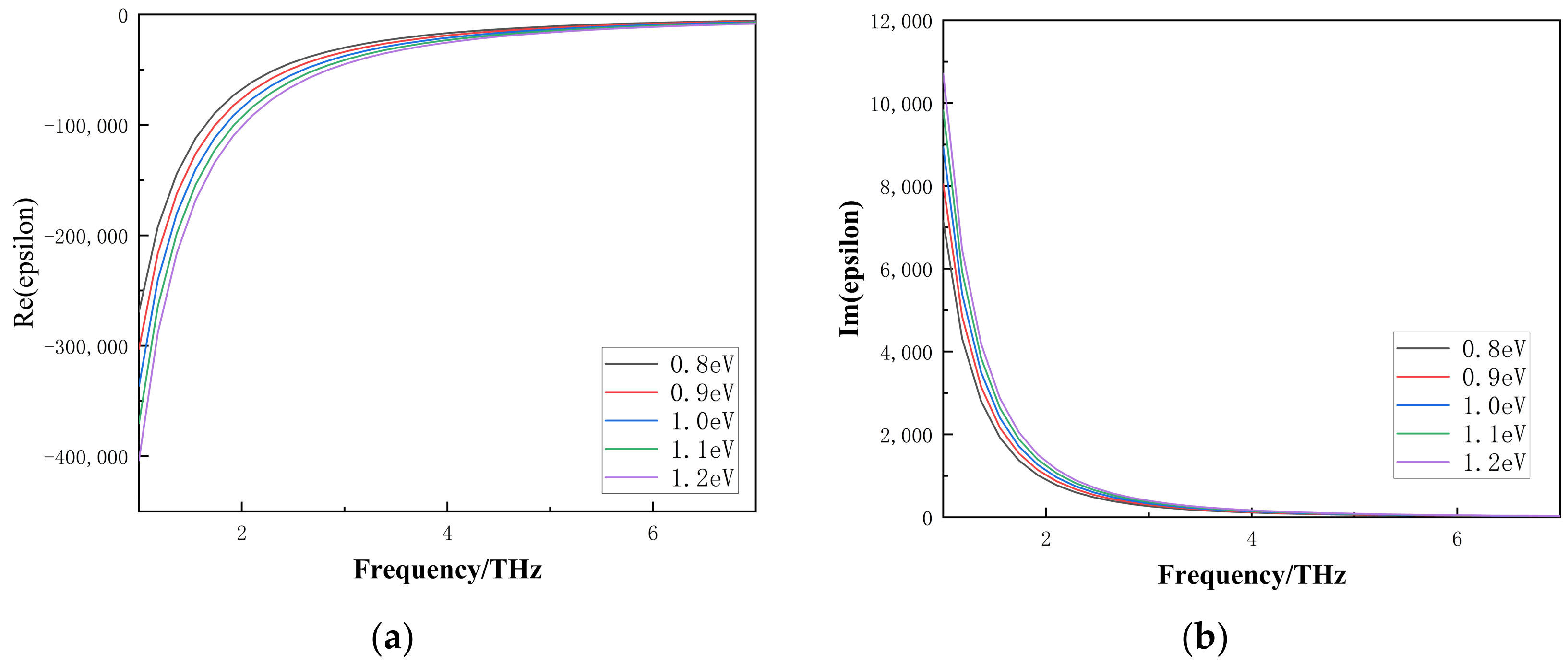
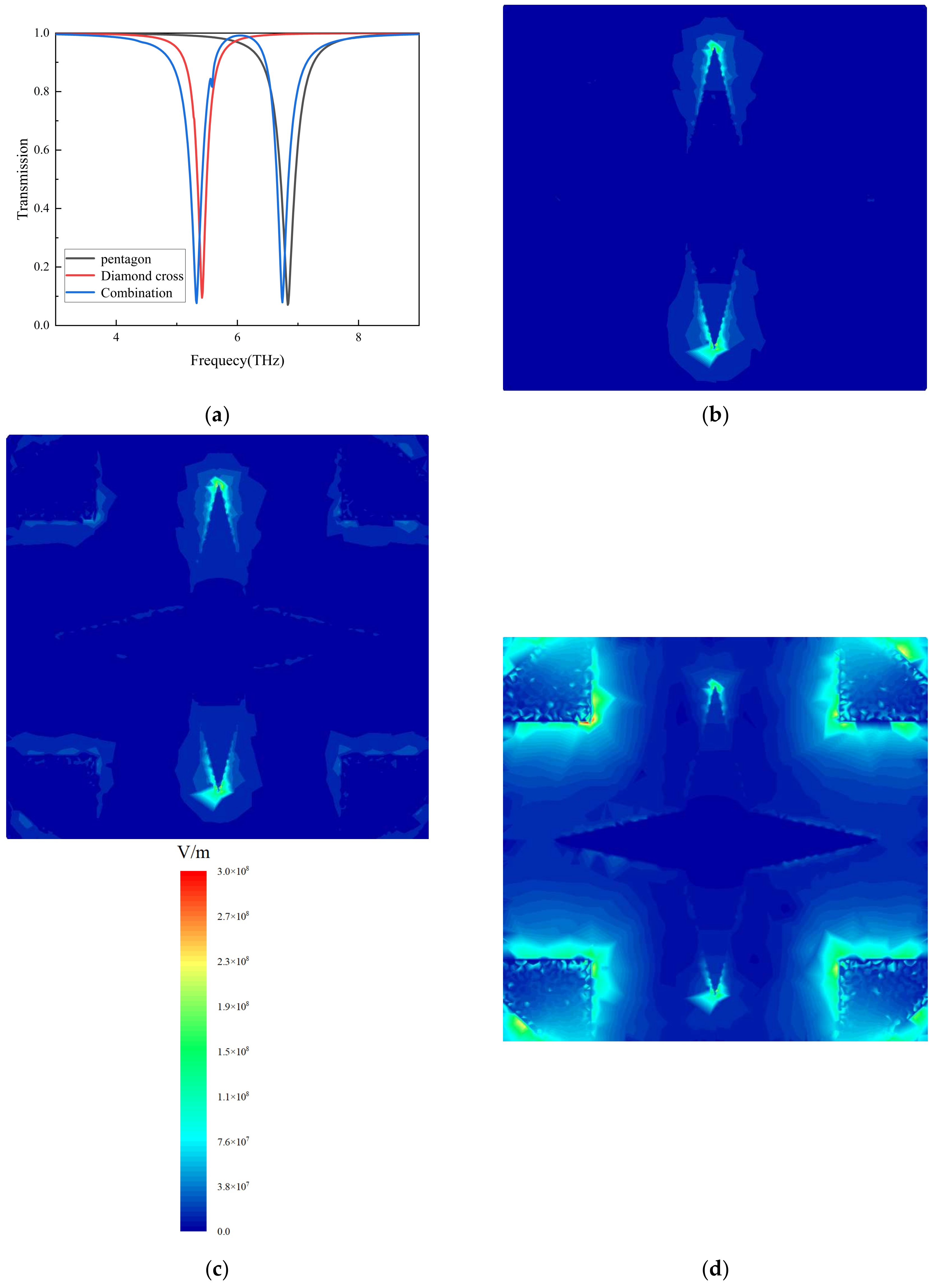
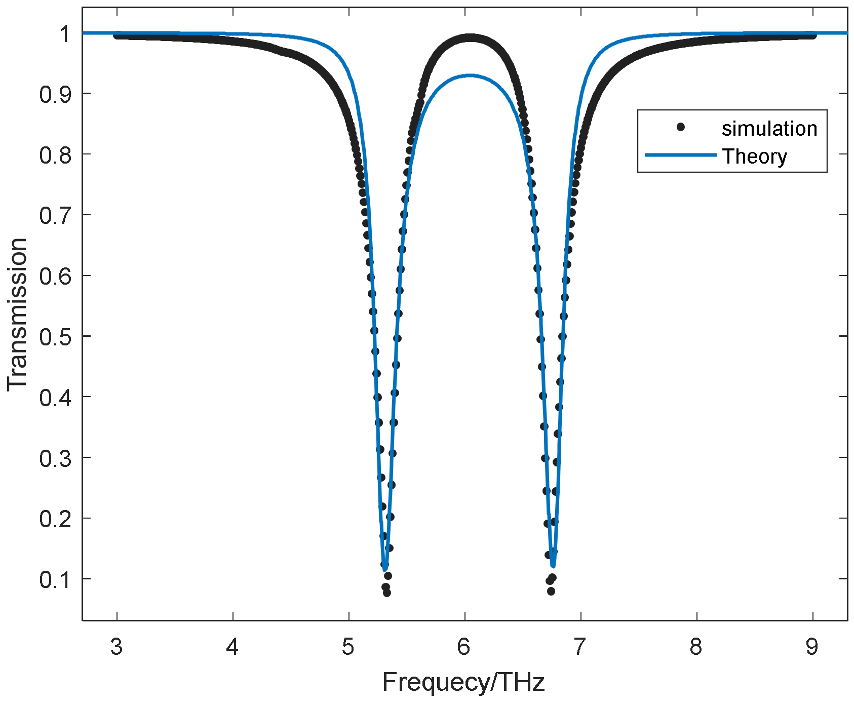
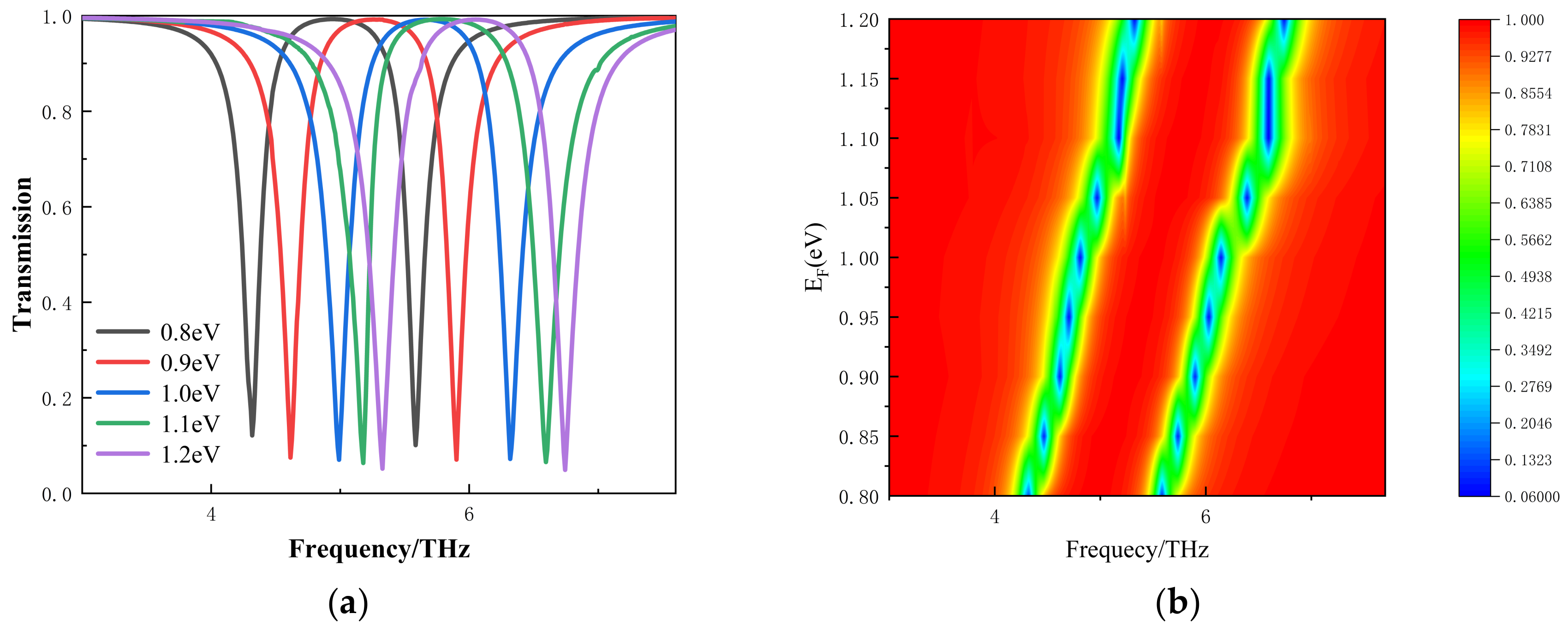
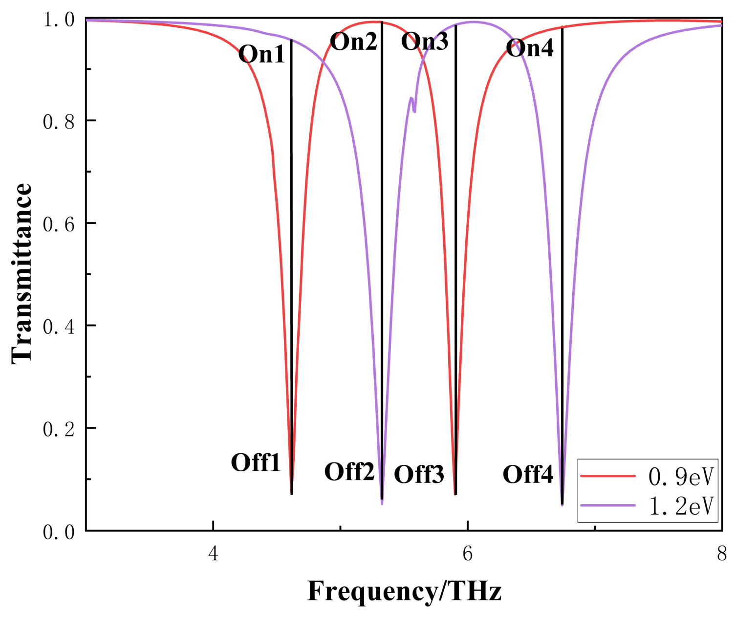
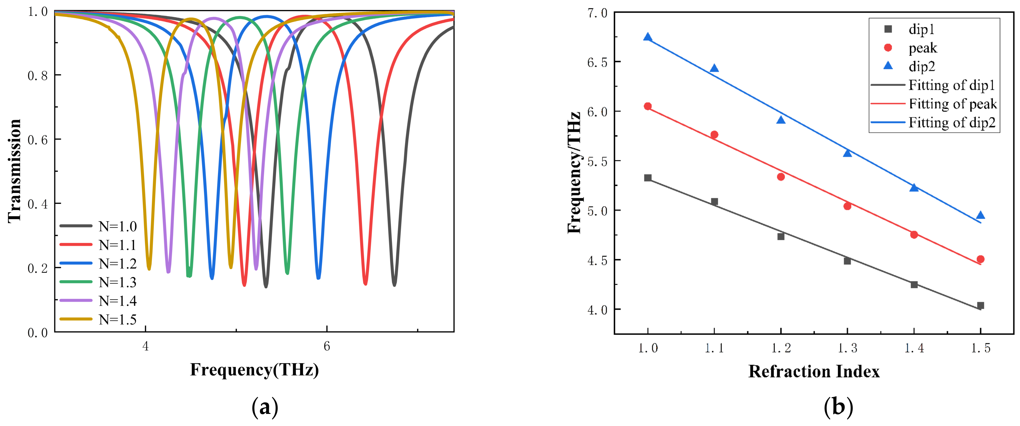
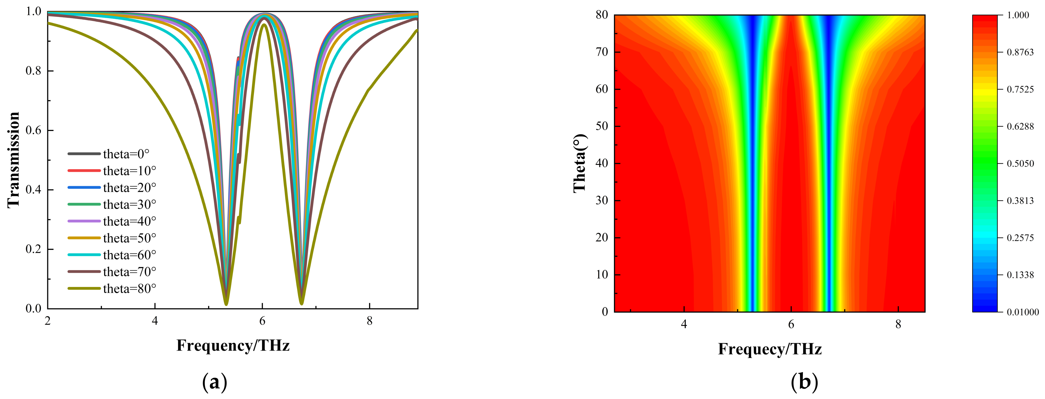
3. Results and Discussions

The transmission spectrum of the structure we designed is shown in Figure 3a. The figure also includes the spectra of a single diamond-shaped cross graphene resonator and pentagon graphene located at the edge, which were studied and compared. In our proposed graphene metasurface, we can observe a significant PIT phenomenon at 6 terahertz, indicated by the blue line in the figure. The black line represents a single transmission peak generated solely by the diamond-shaped cross graphene monomer structure, while the red line represents a single transport valley generated solely from pentagon graphene unit structure. The transmission valleys of the diamond-shaped cross and pentagon graphene resonators are located at 5.3 and 6.7 terahertz, respectively, as two bright modes. The electric field distribution at each resonance point is shown in Figure 3b–d. For structures consisting only of pentagon and diamond-shaped graphene, each resonant cavity directly interacts with the incident wave, appearing as two dipoles in Figure 3b,d. However, in composite structures, the electric field redistributes, and strong coupling occurs between the two resonant cavities, as shown in Figure 3c. As a result, the PIT transparent window is caused by the destructive interference of the two bright modes.
To provide a clearer understanding of the formation process of the PIT transparent window, we utilized the Lorentz oscillation coupling model to fit the parameters into the simulation results. In this coupling model, we represent the incident plane wave as E, the resonant cavity of mode 1 as M 1 ~ , and the resonant cavity of mode 2 as M 2 ~ . As per the definition, the Lorentz oscillation coupling model, when coupled in bright mode, can be expressed as follows [41]:
ω ω 1 + i γ 1 k ~ k ~ ω ω 2 + i γ 2 M 1 ~ M 2 ~ = g 1 E ~ g 2 E   ~
Due to the energy dissipation of metamaterial structures being primarily determined by the imaginary part of magnetic permeability, the transmittance of graphene metamaterial structures can be expressed simply as follows:
T ω = 1 M 1 ~ E ~ 2 = 1 g 1 ω ω 2 + i γ 2 g 2 k ~ E ~ ω ω 1 + i γ 1 ω ω 2 + i γ 2 k ~ 2 2
The numerical fitting results are illustrated by the blue line in Figure 4. The fitted parameters are as follows: E ~ = 0.5988, ω 1 = 5.329, ω 2 = 6.714, g 1 = 0.0061, g 2 = 1.2823, k = 0.186, γ 1 = 0.1073, and γ 2 = 0.1036. This figure demonstrates a strong correspondence between the Lorentz oscillation coupling model and the numerical simulation results. This finding further corroborates the reliability and accuracy of the simulated PIT curve.
Figure 5a,b analyze the tunable transmission spectra of our designed graphene metasurface at different Fermi levels. As the Fermi level increases from 0.8 to 1.2 eV, the entire transmission spectrum shifts towards the high-frequency region. This phenomenon is consistent with the relationship between frequency ( f ) and Fermi level ( E f ) f E f α 0   2 π 2 c L [30]. According to the formula α0 = e2/ℏ, where α0 is the structural constant of graphene, and L is the length of the graphene ribbon, the resonant frequency will increase with the increase of the Fermi level. This allows for the tunable function of the device using different Fermi levels. To adjust the Fermi level and carrier concentration of the entire graphene in the laboratory, a metal electrode will be installed in the graphene layer in order to excite different Fermi levels.
The relationship between the gate voltage Ev and its controlled graphene Fermi level μc could be expressed as shown in Equation (8) [42,43].
μ c = V F π ε 0 ε d E v e d 0
In the equation, ℏ, V F , ε 0 , ε d , e , d 0 are the reduced Planck constant, Fermi velocity of graphene, dielectric constant of vacuum, dielectric constant of substrate, electron charge, and substrate thickness, respectively. The Fermi velocity of graphene is 1.0 × 10⁶ m/s.
Our proposed graphene metasurface can achieve a four-frequency switching modulator. In this example, the lower limit of the Fermi level is set to EF = 0.9 eV, and the upper limit is set to EF = 1.2 eV, which serves as the reference. We assume a carrier mobility of graphene of 1.8 m2/vs. As shown in Figure 6, the frequencies of the four-frequency optical switch are set at 4.6 terahertz, 5.3 terahertz, 5.9 terahertz, and 6.7 terahertz, respectively. The state of the optical switch changes simultaneously with the Fermi level. Therefore, these four optical switches are synchronized. Modulation depth (MD = (Ton-Toff)/(Ton) × 100%), insertion loss (IL = −10log10(Ton)), and extinction ratio (ER = 10log10(Ton/Toff)) are three important parameters for evaluating the performance of switch modulators. The modulation depth (MD) values calculated for the four switches are 92.15%, 94.79%, 92.82%, and 95.04%, respectively. The corresponding insertion losses (IL) are 0.19 dB, 0.04 dB, 0.06 dB, and 0.08 dB, respectively. The corresponding extinction ratios (ER) are 11.05 dB, 12.83 dB, 11.44 dB, and 13.00 dB. Table 1 presents a performance comparison between our design and designs proposed in other recent literature. From Table 1, it is evident that our designed optical switch outperforms others in terms of modulation depth, insertion loss, and extinction ratio.
In addition, Figure 7 shows the sensing characteristics of the graphene metasurface proposed by us under different surrounding media. Figure 7a shows that as the refractive index (n) increases from 1.0 to 1.5, the PIT spectrum shifts towards the low-frequency region. This shift exhibits a good linear relationship with the refractive index. The performance of the metamaterial structure as a sensor is evaluated using sensitivity, defined as S = Δf/Δn, where Δ f represents the frequency shift of the transmission peak/dip, and Δn represents the shift of the refractive index. By calculating the slope in Figure 7b, we obtained sensitivity values of 2.63 THz/RIU and 3.70 THz/RIU for the two transmission dips, and 3.16 THz/RIU for the transmission peak. Another performance metric used to describe metamaterial sensors is the figure of merit (FOM), which can be determined using FOM = S/FWHM. The FWHM represents the full width at half maximum. After calculation, the designed sensor achieved an FOM of 22.397 RIU-1. Table 2 compares the performance of our designed sensor with other literature in recent years. From Table 2, it is evident that our designed sensor exhibits more sensitive sensing performance and a higher FOM.
We discussed the modulation of the PIT transparent window in Figure 8a,b with different structural parameters r1 and r2. For graphene, we chose the Fermi level EF = 1.2 eV and carrier mobility μ = 1.5 m2/vs. In Figure 8a, as r1 increases, dip1 redshifts and the PIT transparent window widens. In Figure 8b, as r2 increases, dip1 blue shifts and the PIT transparent window narrows. These phenomena indicate that the size of r1 and r2 will affect the resonant frequency of dip1. The LC resonance theory can explain these phenomena. The periodic graphene units in metasurfaces can be viewed as a combination of capacitive, inductive, and resistive elements. The resonant frequency of these graphene units with incident light is inversely proportional to the length of graphene and directly proportional to its width.
Moreover, we also discuss the influence of the incident angle on metasurfaces. In experiments, it is challenging to achieve a situation where the incident wave is completely perpendicular to the metasurface. The incident wave has a certain angle with the z-axis, which may affect the observed data to some extent. To investigate the effect of the incident angle on the properties of metasurfaces, we varied the incident angle to study the changing characteristics of metasurfaces. We analyzed the impact of oblique incidence on plasmon-induced transparency in Figure 9a,b. Let us denote the incident angle of the electromagnetic wave as α, representing the angle between the incident direction and the z-axis. When the incident angle is adjusted from 0° to 60°, the transmittance is minimally affected. However, when the incident angle exceeds 60°, the transmittance decreases at all frequencies within the range of 2–9 THz, while the position of the PIT window remains unchanged. This effect is attributed to the reduced coupling between these two bright modes as the incident angle increases. Therefore, our proposed graphene metasurface design demonstrates insensitivity to changes in the incident angle within the terahertz range. This characteristic allows for the application of our proposed metasurface in experimental environments with incident angle errors and provides greater adaptability.

4. Conclusions

In summary, we have designed a graphene metasurface that achieves a tunable PIT effect. This effect is caused by the coupling of bright modes in each graphene resonant cavity. Transparent windows can be accurately fitted using the Lorentz model. By varying the Fermi levels, carrier mobility, and oblique incidence angles, we can effectively generate tunable PIT effects. Additionally, we have discussed the impact of different Fermi levels on the transmission spectra of our proposed metasurface. Furthermore, our graphene metasurface can function as a four-frequency switch modulator and a high-sensitivity sensor in the terahertz band. In terms of optical switches, we have achieved a maximum MD of 95.04%, a minimum IL of 0.08 dB, and a maximum ER of 13 dB. As for sensing capabilities, we have achieved a maximum sensitivity of 3.70 THz/RIU and a maximum FOM of 22.40 RIU−1. These physical properties demonstrate that our metasurface not only exhibits excellent sensing performance, but also enables high-performance multi-frequency switching. Therefore, this study holds significant potential for the application of tunable metasurfaces. Furthermore, the research results may pave the way for the design and manufacture of ultra-sensitive sensors, tunable filters, and other related optoelectronic devices.

Author Contributions

Conceptualization, A.Z. and M.Z.; methodology, A.Z.; investigation, L.C.; writing—original draft, A.Z. and M.Z.; writing—review & editing, A.Z., M.Z. and C.H.; project administration, C.X.; Funding acquisition, W.H. All authors have read and agreed to the published version of the manuscript.

Funding

This work was supported in part by the National Natural Science Foundation of China (62461011), Guangxi Natural Science Foundation (2025GXNSFAA069299), Guangxi Key Laboratory of Automatic Detecting Technology and Instruments (YQ22110), Shanxi Province Science and Technology Major Program (202201030201009), the Open Project Program of Shanxi Key Laboratory of Advanced Semiconductor Optoelectronic Devices and Integrated Systems (2023SZKF04), and a grant from Guangxi Key Laboratory of Brain-inspired Computing and Intelligent Chips (BCIC-24-K1).

Institutional Review Board Statement

Not applicable.

Informed Consent Statement

Not applicable.

Data Availability Statement

The data supporting the findings of this study are available within the article.

Conflicts of Interest

The authors declare no conflicts of interest.

References

  1. Huang, P.; Yao, Y.; Zhong, W.; Gu, P.; Yan, Z.; Liu, F.; Yan, B.; Tang, C.; Chen, J.; Zhu, M. Optical sensing based on classical analogy of double Electromagnetically induced transparencies. Results Phys. 2022, 39, 105732. [Google Scholar] [CrossRef]
  2. Jamshidi, M.; Park, C.B.; Azhari, F. An EIT-based piezoresistive sensing skin with a lattice structure. Mater. Des. 2023, 233, 112227. [Google Scholar] [CrossRef]
  3. Li, J.-S.; Xue, Y.-Y.; Guo, F.-L. Triple frequency bands terahertz metasurface sensor based on EIT and BIC effects. Opt. Commun. 2023, 554, 130225. [Google Scholar] [CrossRef]
  4. Foong, L.K.; Shabani, M.; Sharghi, A.; Reihanisaransari, R.; Al-Bahrani, M.; Le, B.N.; Khalilian, A. Electromagnetically induced transparency for efficient optical modulation in a graphene-dielectric metasurface with surface roughness. Surfaces Interfaces 2022, 35, 102423. [Google Scholar] [CrossRef]
  5. Lu, Z.; Yuan, J.; Xu, G.; Luo, B.; Tan, J. Optically implemented deep terahertz switch based on perovskite film and electromagnetically induced transparency metasurface. Opt. Laser Technol. 2024, 183, 112303. [Google Scholar] [CrossRef]
  6. Chen, Y.; Duan, G.; Xu, C.; Qin, X.; Zhao, Q.; Zhou, H.; Wang, B.-X. Triple-band graphene-based tunable electromagnetically induced transparency terahertz metamaterial with multi-frequency optical switching. Diam. Relat. Mater. 2024, 143, 110939. [Google Scholar] [CrossRef]
  7. Wang, Z.; Yang, F.; Zhou, P.; Zhang, X.; Yang, Y.; Yan, X.; Gao, S.; Zong, M.; Wang, M.; Yao, H.; et al. Frequency-tunable hybrid metamaterial terahertz logic gate with liquid crystal based on electromagnetically induced transparency. Results Phys. 2023, 56, 107295. [Google Scholar] [CrossRef]
  8. Wang, Y.; He, Z.; Cui, W.; Ren, X.; Li, C.; Xue, W.; Cao, D.; Li, G.; Lei, W. Tunable plasmon induced transparency in the ellipse-shaped resonators coupled waveguide. Results Phys. 2020, 16, 102981. [Google Scholar] [CrossRef]
  9. Tassin, P.; Zhang, L.; Koschny, T.; Economou, E.N.; Soukoulis, C.M. Low-Loss Metamaterials Based on Classical Electromagnetically Induced Transparency. Phys. Rev. Lett. 2009, 102, 053901. [Google Scholar] [CrossRef]
  10. Liang, D.; Chen, T. Optical modulated graphene metamaterial based on plasmon-induced transparency in the terahertz band: Application for sensing. Diam. Relat. Mater. 2022, 131, 109613. [Google Scholar] [CrossRef]
  11. Guo, X.; Cong, J.; Li, C. Dynamic tunable multiple plasmon induced transparency sensor and optical switch in dual-polarization excitation in a terahertz graphene metamaterial. Opt. Commun. 2023, 551, 130058. [Google Scholar] [CrossRef]
  12. Xiang, J.; Chen, T. A triple plasmon-induced transparency terahertz sensor based on graphene metamaterials. Diam. Relat. Mater. 2024, 149, 111608. [Google Scholar] [CrossRef]
  13. Meng, Q.; Chen, F.; Xu, Y.; Cheng, S.; Yang, W.; Yao, D.; Yi, Z. Multi-frequency polarization and electro-optical modulator based on triple plasmon- induced transparency in monolayer graphene metamaterials. Diam. Relat. Mater. 2023, 138, 110216. [Google Scholar] [CrossRef]
  14. Dai, C.; Li, B.; Zeng, L.; Wang, Q.; Chen, Z.; Zeng, Y.; Zhang, X.; Deng, C. Graphene modulator and 2-bit encoder based on plasma induced transparency effect. Diam. Relat. Mater. 2024, 150, 111715. [Google Scholar] [CrossRef]
  15. Zhu, A.; Li, Z.; Hou, W.; Cheng, L.; Hu, C.; Zhao, T.; Xu, C.; Mahapatra, R. Double plasmon-induced transparency 3 bit graphene encoder. Diam. Relat. Mater. 2024, 142, 110800. [Google Scholar] [CrossRef]
  16. Zhu, A.; Li, Z.; Hou, W.; Yang, X.; Cheng, L.; Hu, C.; Qiao, F.; Mahapatra, R. A 2-bit graphene encoder based on the plasmon-induced transparency effect and its sensing characteristics. Results Phys. 2024, 59, 107608. [Google Scholar] [CrossRef]
  17. Yu, N.; Capasso, F. Flat optics with designer metasurfaces. Nat. Mater. 2014, 13, 139–150. [Google Scholar] [CrossRef]
  18. Chen, S.; Li, Z.; Liu, W.; Cheng, H.; Tian, J. From Single-Dimensional to Multidimensional Manipulation of Optical Waves with Metasurfaces. Adv. Mater. 2019, 31, 1802458. [Google Scholar] [CrossRef]
  19. Yu, N.; Genevet, P.; Kats, M.A.; Aieta, F.; Tetienne, J.-P.; Capasso, F.; Gaburro, Z. Light Propagation with Phase Discontinuities: Generalized Laws of Reflection and Refraction. Science 2011, 334, 333–337. [Google Scholar] [CrossRef]
  20. Zhong, F.; Li, J.; Liu, H.; Zhu, S. 12-Photon Entanglement and Scalable Scattershot Boson Sampling with Optimal Entangled-Photon Pairs from Parametric Down-Conversion. Phys. Rev. Lett. 2018, 120, 243901. [Google Scholar] [CrossRef]
  21. Su, Z.; Yang, Y.; Xiong, B.; Zhao, R.; Wang, Y.; Huang, L. Planar Chiral Metasurface Based on Coupling Quasi-Bound States in the Continuum. Adv. Opt. Mater. 2024, 12, 2303195. [Google Scholar] [CrossRef]
  22. Shao, Y.; Su, Z.; He, H.; Jing, X.; Liu, Y.; Geng, G.; Li, J.; Wang, Y.; Huang, L. Multispectral imaging through metasurface with quasi-bound states in the continuum. Opt. Express 2024, 32, 23268–23279. [Google Scholar] [CrossRef] [PubMed]
  23. Huang, L.; Chen, X.; Mühlenbernd, H.; Zhang, H.; Chen, S.; Bai, B.; Tan, Q.; Jin, G.; Cheah, K.-W.; Qiu, C.-W.; et al. Three-dimensional optical holography using a plasmonic metasurface. Nat. Commun. 2013, 4, 2808. [Google Scholar] [CrossRef]
  24. Pu, M.; Chen, P.; Wang, C.; Wang, Y.; Zhao, Z.; Hu, C.; Huang, C.; Luo, X. Broadband anomalous reflection based on gradient low-Q meta-surface. AIP Adv. 2013, 3, 052136. [Google Scholar] [CrossRef]
  25. Lopato, P.; Herbko, M.; Gora, P.; Mescheder, U.; Kovacs, A.; Filbert, A. Numerical Analysis of the Influence of Fabrication Process Uncertainty on Terahertz Metasurface Quality. Electronics 2023, 12, 2198. [Google Scholar] [CrossRef]
  26. Seong, J.; Jeon, Y.; Yang, Y.; Badloe, T.; Rho, J. Cost-Effective and Environmentally Friendly Mass Manufacturing of Optical Metasurfaces Towards Practical Applications and Commercialization. Int. J. Precis. Eng. Manuf. Technol. 2023, 11, 685–706. [Google Scholar] [CrossRef]
  27. Fan, Y.; Shen, N.; Zhang, F.; Zhao, Q.; Wu, H.; Fu, Q.; Wei, Z.; Li, H.; Soukoulis, C.M. Graphene Plasmonics: A Platform for 2D Optics. Adv. Opt. Mater. 2018, 7, 1800537. [Google Scholar] [CrossRef]
  28. Nan, J.; Zhang, Y.; Xie, Y.; Li, Z.; Yang, R.; Xu, J.; Fu, Q.; Zhang, F.; Fan, Y. Coupling Controlled Dual-Band Tunable Electromagnetic Extraordinary Transmission in Graphene Hybrid Metasurfaces. Adv. Electron. Mater. 2023, 9, 2300065. [Google Scholar] [CrossRef]
  29. Liu, Z.; Yang, G.; Luo, X.; Zhou, F.; Cheng, Z.; Yi, Z. Tunable quintuple plasmon-induced transparency and the effect of symmetry breaking based on monolayer graphene split rings metasurface. Diam. Relat. Mater. 2024, 142, 110786. [Google Scholar] [CrossRef]
  30. Xie, Q.; Guo, L.; Zhang, Z.; Gao, P.; Wang, M.; Xia, F.; Zhang, K.; Sun, P.; Dong, L.; Yun, M. Versatile terahertz graphene metasurface based on plasmon-induced transparency. Appl. Surf. Sci. 2022, 604, 154575. [Google Scholar] [CrossRef]
  31. Wang, Y.; Chang, B.; Xue, J.; Cao, X.; Xu, H.; He, H.; Cui, W.; He, Z. Sensing and slow light applications based on graphene metasurface in terahertz. Diam. Relat. Mater. 2022, 123, 108881. [Google Scholar] [CrossRef]
  32. Xu, Y.; Xu, H.; Jiang, X.; Yin, J. Versatile Functionalization of the Micropatterned Hydrogel of Hyperbranched Poly(ether amine) Based on “Thiol-yne” Chemistry. Adv. Funct. Mater. 2014, 24, 1679–1686. [Google Scholar] [CrossRef]
  33. Yang, R.; Zhang, L.; Wang, Y.; Shi, Z.; Shi, D.; Gao, H.; Wang, E.; Zhang, G. An Anisotropic Etching Effect in the Graphene Basal Plane. Adv. Mater. 2010, 22, 4014–4019. [Google Scholar] [CrossRef] [PubMed]
  34. Jia, W.; Ren, P.-W.; Tian, Y.-C.; Fan, C.-Z. Dynamically tunable optical properties in graphene-based plasmon-induced transparency metamaterials. Chin. Phys. B 2019, 28, 026102. [Google Scholar] [CrossRef]
  35. Chen, D.-C.; Li, H.-J.; Xia, S.-X.; Qin, M.; Zhai, X.; Wang, L.-L. Dynamically tunable electromagnetically-induced-transparency-like resonances in graphene nanoring and nanodisk hybrid metamaterials. EPL Europhys. Lett. 2017, 119, 47002. [Google Scholar] [CrossRef]
  36. Tian, Y.-C.; Jia, W.; Ren, P.-W.; Fan, C.-Z. Tunable plasmon-induced transparency based on asymmetric H-shaped graphene metamaterials. Chin. Phys. B 2018, 27, 124205. [Google Scholar] [CrossRef]
  37. Liu, T.; Wang, H.; Liu, Y.; Xiao, L.; Zhou, C.; Xu, C.; Xiao, S. Dynamically tunable electromagnetically induced transparency in a terahertz hybrid metamaterial. Phys. E Low-Dimens. Syst. Nanostruct. 2018, 104, 229–232. [Google Scholar] [CrossRef]
  38. Zhou, F.; Wang, Y.; Zhang, X.; Wang, J.; Liu, Z.; Luo, X.; Zhang, Z.; Gao, E. Dynamically adjustable plasmon-induced transparency and switching application based on bilayer graphene metamaterials. J. Phys. D Appl. Phys. 2020, 54, 054002. [Google Scholar] [CrossRef]
  39. Li, Y.; Xu, Y.; Jiang, J.; Ren, L.; Cheng, S.; Wang, B.; Zhou, X.; Wang, Z. Dual dynamically tunable plasmon-induced transparency and absorption in I-type-graphene-based slow-light metamaterial with rectangular defect. Optik 2021, 246, 167837. [Google Scholar] [CrossRef]
  40. Hu, F.; Fan, Y.; Zhang, X.; Jiang, W.; Chen, Y.; Li, P.; Yin, X.; Zhang, W. Intensity modulation of a terahertz bandpass filter: Utilizing image currents induced on MEMS reconfigurable metamaterials. Opt. Lett. 2018, 43, 17–20. [Google Scholar] [CrossRef]
  41. Tang, B.; Jia, Z.; Huang, L.; Su, J.; Jiang, C. Polarization-Controlled Dynamically Tunable Electromagnetically Induced Transparency-Like Effect Based on Graphene Metasurfaces. IEEE J. Sel. Top. Quantum Electron. 2020, 27, 4700406. [Google Scholar] [CrossRef]
  42. Chen, H.; Zhang, Z.; Yang, J.; Zhou, Z. Controlled and tunable plasmon-induced transparency based on graphene metasurfaces in atmospheric windows. Diam. Relat. Mater. 2022, 127, 109210. [Google Scholar] [CrossRef]
  43. Agravat, D.; Patel, S.K.; Almawgani, A.H.M.; Alsuwian, T.; Armghan, A.; Daher, M.G. Investigation of a Novel Graphene-Based Surface Plasmon Resonance Solar Absorber to Achieve High Absorption Efficiency Over a Wide Spectrum of Wavelengths, from Ultraviolet to Infrared. Plasmonics 2023, 19, 1071–1083. [Google Scholar] [CrossRef]
  44. Zhu, J.; Xiong, J. Tunable terahertz graphene metamaterial optical switches and sensors based on plasma-induced transparency. Measurement 2023, 220, 113302. [Google Scholar] [CrossRef]
  45. Qin, Y.; Zhou, F.; Liu, Z.; Zhang, X.; Zhuo, S.; Luo, X.; Ji, C.; Yang, G.; Zhou, Z.; Sun, L.; et al. Triple plasmon-induced transparency and dynamically tunable electro-optics switch based on a multilayer patterned graphene metamaterial. J. Opt. Soc. Am. A 2022, 39, 377–382. [Google Scholar] [CrossRef]
  46. Meng, Q.; Chen, F.; Xu, Y.; Cheng, S.; Yang, W.; Yao, D.; Yi, Z. Tunable terahertz double plasmon induced-transparency based on monolayer patterned graphene structure. Photonics Nanostruct. Fundam. Appl. 2023, 54, 101132. [Google Scholar] [CrossRef]
  47. Wu, Z.; An, P.; Ding, M.; Qi, Y.; Zhang, L.; Han, S.; Lian, D.; Chen, C.; Yang, X. Tunable Electromagnetically Induced Transparent Window of Terahertz Metamaterials and Its Sensing Performance. Appl. Sci. 2022, 12, 7057. [Google Scholar] [CrossRef]
  48. Li, J.; Weng, J.; Li, J.; Chen, S.; Guo, Z.; Xu, P.; Liu, W.; Wen, K.; Qin, Y. Dynamic manipulation of plasmon induced transparency with parallel-orthometric graphene strips structure. Results Phys. 2022, 40, 105816. [Google Scholar] [CrossRef]
  49. Li, G. Tunable Fano resonance for advanced sensing in graphene-based metasurface. Diam. Relat. Mater. 2024, 142, 110823. [Google Scholar] [CrossRef]
  50. Li, Z.; Yang, N.; Liu, Y.; Zhong, Z.; Song, C.; He, Z.; Cui, W.; Xue, W.; Li, L.; Li, C.; et al. Tunable plasmonic optical responses and the sensing application in graphene-based metasurface. Diam. Relat. Mater. 2022, 126, 109071. [Google Scholar] [CrossRef]
  51. He, Z.; Cui, W.; Ren, X.; Li, C.; Li, Z.; Xue, W.; Zhang, B.; Zhao, R. Ultra-high sensitivity sensing based on tunable plasmon-induced transparency in graphene metamaterials in terahertz. Opt. Mater. 2020, 108, 110221. [Google Scholar] [CrossRef]
  52. Wang, M.; Cui, W.; Wang, Y.; Li, M.; Qie, X. Tunable fano-like resonances in graphene metasurface for quad-frequency optoelectronic sensing. Phys. E Low-Dimens. Syst. Nanostruct. 2025, 168, 116191. [Google Scholar] [CrossRef]
  53. Tan, C.; Wang, S.; Li, S.; Liu, X.; Wei, J.; Zhang, G.; Ye, H. Cancer Diagnosis Using Terahertz-Graphene-Metasurface-Based Biosensor with Dual-Resonance Response. Nanomaterials 2022, 12, 3889. [Google Scholar] [CrossRef] [PubMed]
Figure 1. (a) schematic diagram of unit structure; (b) vertical view of cell structure.
Photonics 12 00218 g001
Figure 2. (a) the real parts of permittivity for graphene in different chemical potentials.; (b) the imaginary parts of permittivity for graphene in different chemical potentials.
Photonics 12 00218 g002
Figure 3. (a) transmission spectrum of graphene metasurface; (bd) the normalized electric field distribution at the frequency of 5.3 THz, 6.0 THz, and 6.7 THz.
Photonics 12 00218 g003
Figure 4. The transmission of our proposed graphene metasurface in THz region. The black dotted line indicates numerical simulation result and the blue solid line represents the Lorentz oscillation coupling model calculation result.
Photonics 12 00218 g004
Figure 5. (a,b) transmittance spectra with different Fermi energies in the THz region.
Photonics 12 00218 g005
Figure 6. Four-frequency switching modulator modulation of the transmittance spectra when EF is set as 0.9 eV and 1.2 eV.
Photonics 12 00218 g006
Figure 7. (a) transmission spectra with different refraction indices of the surrounding medium; (b) linear fit of resonant peak with different refractive indices.
Photonics 12 00218 g007
Figure 8. (a) transmission spectra with r1 from 2.1 μm to 2.7 μm; (b) transmission spectra with r2 from 0.6 μm to 1.0 μm.
Photonics 12 00218 g008
Figure 9. (a,b) transmission spectra with various incident angles.
Photonics 12 00218 g009
Table 1. Comparison of performance with other terahertz optical switch.
MD (%)IL (dB)ER (dB)Ref
95.60.315/[44]
94.3/12.43[45]
94.51.3607.77[46]
93.30.25011.75[47]
89.00.55/[48]
95.040.0813.00This work
Table 2. Comparison of sensing performance in our design with other graphene-based sensors.
Structure Sensitivity (THz/RIU) FOM (max) Ref
Graphene1.1/[49]
Graphene3.426921.92[50]
Graphene0.79288.12[31]
Graphene1.71346.998[51]
Graphene1.4017.30[10]
Graphene1.842444.27[52]
Graphene1.212.75[53]
Graphene3.7022.40This work
Disclaimer/Publisher’s Note: The statements, opinions and data contained in all publications are solely those of the individual author(s) and contributor(s) and not of MDPI and/or the editor(s). MDPI and/or the editor(s) disclaim responsibility for any injury to people or property resulting from any ideas, methods, instructions or products referred to in the content.

