Article

Flat Emission Silicon Nitride Grating Couplers for Lidar Optical Antennas

by
Thenia Prousalidi
1,*,
Georgios Syriopoulos
1,
Evrydiki Kyriazi
1,
Roel Botter
2,
Charalampos Zervos
1,
Giannis Poulopoulos
1 and
Dimitrios Apostolopoulos
1
1
School of Electrical and Computer Engineering, National Technical University of Athens, 15780 Zografou, Greece
2
Lionix BV International, Hengelosestraat 500, 7521 AN Enschede, The Netherlands
*
Author to whom correspondence should be addressed.
Photonics 2025, 12(3), 214; https://doi.org/10.3390/photonics12030214
Submission received: 31 January 2025 / Revised: 22 February 2025 / Accepted: 25 February 2025 / Published: 28 February 2025

Abstract

:
Light detection and ranging (Lidar) is a key enabling technology for autonomous vehicles and drones. Its emerging implementations are based on photonic integrated circuits (PICs) and optical phased arrays (OPAs). In this work, we introduce a novel approach to the design of OPA Lidar antennas based on Si3N4 grating couplers. The well-established TriPleX platform and the asymmetric double stripe waveguide geometry with full etching are employed, ensuring low complexity and simple fabrication combined with the low-loss advantages of the platform. The design study aims to optimize the performance of the grating coupler-based radiators as well as the OPA, thus enhancing the overall capabilities of Si3N4-based Lidar. Uniform and non-uniform grating structures are considered, achieving θ and φ angle divergences of 0.9° and 32° and 0.54° and 25.41°, respectively. Also, wavelength sensitivity of 7°/100 nm is achieved. Lastly, the fundamental OPA parameters are investigated, and 35 dBi of peak directivity is achieved for an eight-element OPA.

1. Introduction

Autonomous vehicles, terrestrial and airborne, have gained popularity in recent years, with automation use spreading across multiple sectors and industries. Their existing and foreseen applications range from the automotive and mobility industry, with self-driving cars and automated taxis, to aerospace (automated urban air mobility (UAM) scenarios) and drones [1], smart cities, logistics, manufacturing, industrial applications and healthcare [2]. Since autonomous vehicles operate in dynamic environments, they rely on the use of advanced sensorial technologies for mapping [3], like radio detection and ranging (Radar) and light detection and ranging (Lidar). Extensive research has taken place in recent years to advance the performance of and co-integrate Radar and Lidar sensors for autonomous vehicles [4,5].
Lidar is a three-dimensional (3D) imaging, mapping and remote sensing technique that relies on optical beam shaping and steering [6] and has emerged as a promising solution for autonomous vehicles and drones. High-performance Lidar systems compatible with such applications need to enable long-range power transmission with low-cost, low-power consumption and compact and robust implementations [7]. The high performance relies on an increased field of view (FOV), high angular resolution, small beam divergence and an increased scanning speed [8]. Traditionally, Lidar systems have been based on mechanical implementations with free-space optics and rotating parts [9] that, however, are not compatible with the compact size, low-cost and reliability requirements and have a limited scanning speed [10]. Micro-electromechanical system (MEMS) Lidar is a more compact alternative but with reduced FOV and a vulnerability to mechanical shocks. Solid-state Lidar has emerged in recent years as another technique that provides a scalable and reliable solution that does not include any moving mechanical parts [11]. It includes optical phased arrays (OPAs), where the beam is steered by waveguides instead of moving parts [12], or Flash Lidar, which works like a camera and captures the image by illuminating the whole FOV [11]. However, a tradeoff also exists for these methods, as they exhibit a limited steering angle and detection range, respectively.
In recent years, photonic integrated circuit (PIC)-based Lidar has been gaining momentum [13]. The typical choice for PIC-based Lidar is the silicon-on-insulator (SOI) platform [10,14,15], where the beam shaping and steering are performed by a silicon chip with the help of integrated phase shifters and OPAs based on grating elements. A schematic of an optical antenna in OPA configuration based on grating couplers is shown in Figure 1. This platform offers many advantages. Being compatible with standard mature complementary metal-oxide semiconductor (CMOS) fabrication processes, it enables the development of cost-efficient, low-power, reliable and robust Lidar systems, based on highly integrated OPAs [16]. Compact grating antennas based on one-dimensional (1D) OPAs can achieve two-dimensional (2D) beam steering by wavelength tuning along the longitudinal direction and by phase control along the lateral dimension [16,17]. The inherent ultra-high index contrast of the SOI platform allows for beam steering as high as 15° with 100 nm wavelength tuning [18]. However, silicon (Si) PICs require the precise control of their component dimensions for optimal performance and are therefore susceptible to fabrication process errors. Moreover, the SOI platform cannot support high input power levels due to the appearance of non-linear effects in Si, prohibiting its use in high power systems [19]. This limits the application of SOI PIC-based Lidar.
Capitalizing on the advances of SOI-based Lidar, the silicon nitride (Si3N4) platform can enhance and further improve the capabilities and performance of PIC-based Lidar. The Si3N4 platform showcases very low propagation losses and is compatible with high input optical power applications due to its low nonlinearities [20]. In combination with its low index contrast, this platform is robust to fabrication-induced phase variations. Moreover, it is transparent at wavelengths below 1150 nm [21] and showcases reduced emission strength for an increased emitter length and low divergence [22], making it an interesting alternative to SOI for the development of Lidar optical antennas [23]. The Lionix TriPleX waveguide technology is one of the most well-established Si3N4 platforms. Among the different waveguide geometries it offers [24], the asymmetric double stripe (ADS) combines the ultra-low loss advantages of the platform with the lowest minimum bend radii, requiring simpler fabrication processes and offering higher yields compared to other geometries [25]. Moreover, it is compatible with standard multi-project wafer (MPW) fabrication processes employing single etch depth and is highly suitable for applications that require coupling to external components such as active materials. This is especially important for Lidar applications, where the co-integration of the Si3N4 components with other photonic or electronic chips and components (e.g., indium phosphide for the realization of optical sources) can enable the development of complete Lidar and Radar systems.
However, Si3N4 has its own limitations. Adequate beam steering by wavelength tuning remains a challenge due to the limited material dispersion. Recent developments have shown that steering angles of up to 7° for a 100 nm tuning range can be achieved [22]. Moreover, Si3N4-based Lidar is not a mature technology. Although various studies have investigated Si3N4 optical antennas for Lidar [26,27], advances are still required to achieve the desired performance combining low divergence, uniform emission profiles and long length gratings with standard fabrication techniques. This is especially relevant for Si3N4 Lidar antennas employing the ADS waveguide geometry, which have not yet been explored in the literature. However, many applications can benefit from such implementations, thanks to their aforementioned advantages, making research into ADS-based Si3N4 optical radiators highly desirable and impactful.
This paper introduces a new approach to the design of grating couplers (GC) for Lidar optical antennas in the TriPleX Si3N4 platform employing ADS geometry. The effort focuses on achieving the high performance of OPA-based radiators for Lidar systems that can be employed in autonomous vehicles and drones, meeting the demanding requirements of such applications. More specifically, this design study targets a high OPA FOV, increased resolution and low receiver losses. The resolution depends on the beam divergence, and it can be improved by minimizing the beam divergence across the longitudinal and lateral directions (theta (θ) and phi (φ) angle divergences, respectively). The beam divergence is determined by the optical aperture of the antenna and also correlates with the radiation uniformity throughout the antenna length. In general, the θ angle divergence depends on the design of the individual grating elements, while the φ angle divergence depends on the aperture of the OPA. The receiver losses can be reduced by targeting a flat emission profile in the longitudinal direction, achieving gratings with long effective areas (long gratings) that can collect light with increased efficiency. At the same time, this work targets Si3N4 optical radiators that are compatible with simple fabrication processes and a single etch depth, fabricable through MPWs, without requiring access to more advanced techniques. Although this will signify limitations in the achieved performance, it ensures that the designs are low cost and easily fabricable, a requirement necessary in many applications. This is ensured with the use of the ADS geometry with a single full etch depth. The design process outlined in this paper consists of two parts. The first concerns the design and optimization of the single grating element to achieve uniform emissions across the long length and reduce the angle divergence. The second step targets the optimization of the OPA structure.

2. Layerstack and Antenna Design Considerations

The platform for the development of the optical radiators is the Lionix Si3N4 TriPleX platform [24,25] with ADS waveguide geometry. The multiple layers of Si3N4 and silicon dioxide (SiO2) allow low index contrast waveguides to be made, which is beneficial for the reduced sensitivity of the waveguided modes effective refractive index (neff) to the waveguide geometry variation [23]. This results in reduced emission strength and allows long gratings to be achieved. A cross section of the ADS layerstack is shown in Figure 2b. The bottom and top Si3N4 layer thickness is 75 nm and 175 nm, respectively, while the distance between the two layers is 100 nm. The refractive index of the materials is nSiO2 = 1.44537 and nSi3N4 = 1.98350 at 1550 nm. To realize the grating teeth, full etching is employed (removal of both layers of the Si3N4 ADS layerstack), a limitation imposed by the available fabrication process. Adhering to this limitation ensures that the proposed design is fabricable with standard fabrication processes and minimal fabrication risks. As a result, a fixed etching depth is considered. The nominal waveguide width (w) is 1.1 μm; however, this value has been varied in the designed components. The design study was carried out in the spectral range of 1500 nm–1600 nm, centered around 1550 nm.
The proposed GCs serve as the single radiator elements (building blocks) of the optical antenna and act as the light emitters and receivers of the Lidar. They are arranged linearly in series, one next to the other with distance d, in a linear 1D OPA configuration, as shown in Figure 1. Figure 1 illustrates the θ and φ angles along the longitudinal and lateral direction of the OPA, respectively. The 1D OPA can realize beam steering in both directions by tuning the wavelength in the longitudinal direction (θ) and by introducing a phase shift across the grating antenna along the lateral direction (φ). The advantage of this configuration is that 2D beam steering is ensured with a 1D structure, resulting in a significantly reduced footprint (orders of magnitude less) on the chip compared to an equivalent 2D structure, considering that for a given aperture size, 2D OPA requires N2 elements instead of N elements for the 1D OPA. Moreover, in 2D OPAs, the on-chip real estate is increased due to the overhead of the phase shifters required for beam steering in both directions.

3. Design of the Single Radiator Element

The building block of the proposed OPA Lidar optical antenna is the GC. The first part of this study focuses on the design and optimization of the GC-based emitter using the Ansys Lumerical 2023 R2.3 finite-difference eigenmode (FDE) and finite-difference time-domain (FDTD) solvers. Various configurations have been explored, including uniform and non-uniform geometries, to optimize the performance of the single radiator element.

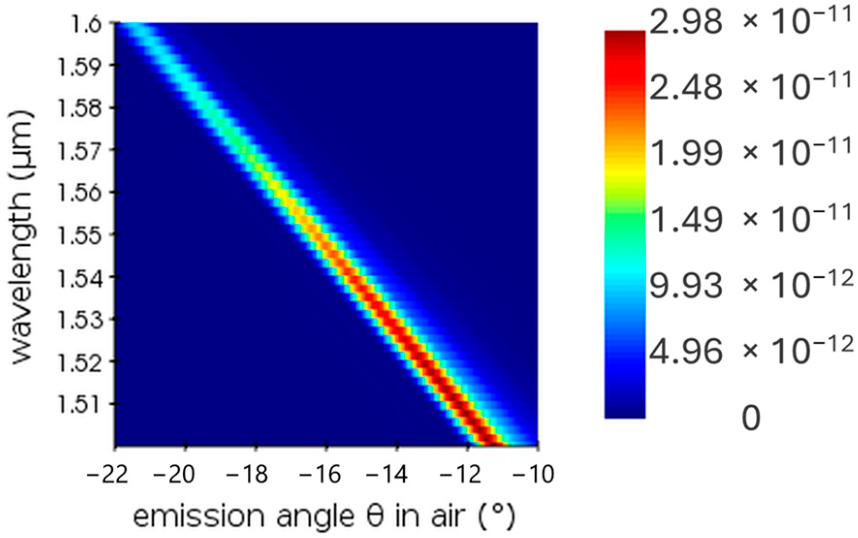
3.1. Principle of Operation

Among the grating parameters, the most relevant for this design study that will be used in the design process are the effective refractive index of the grating period (neff−grating), the emission angle (θ) and the coupling constant (k).
In a grating structure, the effective index of a grating period that consists of an unetched part with effective refractive index of the supported mode n1 and an etched part with effective refractive index of the supported mode n0, with filling factor FF, as shown in Figure 2c, is given by (1):
n e f f g r a t i n g = F F × n 1 + 1 F F × n 0 .
For our structure, since the etched part consists only of SiO2 due to full etching, we assume the effective refractive index in the etched part to be equal to the refractive index of SiO2 (n0 = nSiO2).
The emission angle θ of a grating is related to pitch Λ, the operating wavelength λ and the neff−grating, according to the Bragg condition expressed in (2) [28]:
sin θ = n e f f g r a t i n g λ Λ n S i O 2 .
The coupling constant k expresses the effective refractive index contrast between the high and low index sections of a grating period [27] and is given by (3):
k = n 1 n 0 n e f f g r a t i n g × Λ .
k relates to how fast (over how many periods) the power will be scattered outside the GC. For low-loss waveguide platforms, having low k can help realize GCs with long effective lengths. One way to achieve low k is by varying the waveguide width along the GC length [29]. In applications that target uniform emission profiles, apodization of k along the length is desirable for engineering the emission profile.

3.2. Uniform Design

The simplest GC configuration in terms of design and fabrication complexity is a uniform GC where the geometrical parameters (filling factor (FF), width, pitch (Λ)), chosen for optimal performance, remain constant throughout the GC length. The effective index of the grating (neff−grating), given by (1), is also constant across a uniform design. Uniform GC configurations were investigated and simulated in this study. A top view of the uniform grating is shown in Figure 3.
For the design proposed in this paper, an FF equal to 0.5 was chosen. The next parameter that was investigated was the width. The nominal width in this platform is 1.1 μm, and its minimum value for the proper confinement of the mode in the waveguide is 700 nm. Hence, width values greater than 1 μm were investigated. The waveguide width affects the light confinement within the waveguide in the lateral dimension. At the same time, large width values increase the required distance (d) between adjacent GCs (shown in Figure 1) in the OPA to avoid evanescent-field coupling and crosstalk between the OPA channels. Lastly, as the width increases, we enter the multimode regime, which should be avoided. Therefore, a study of the width impact on the OPA performance (angle divergence) is necessary to optimize its value. To this end, 3D-FDTD simulations were performed, varying the waveguide width between 1 μm and 4 μm with a step of 0.5 μm while keeping the other parameters constant (length = 92.6 μm, FF = 0.5). The simulated θ and φ angle 3 dB divergences are shown in Figure 4a. These results indicate that as the width increases, the φ divergence decreases (10.4% decrease for a width variation between 1 and 4 μm), while θ divergence is monotonically affected (9% increase for a width variation between 1 and 4 μm). Since the θ divergence is close to 1°, this translates to 0.1° of change, which is considered small in terms of absolute value for the application. Taking into account the aforementioned limitations and to ensure that the spacing requirements in the OPA structure remain reasonable, a width of up to 2 μm should be chosen.
As a second step, the effect of the GC length variation is studied to optimize its value. Three-dimensional FDTD was performed, this time varying the GC length between 25 μm and 200 μm while keeping the width constant at 2 μm and the FF at 0.5. The resulting simulated θ and φ angle 3 dB divergences are shown in Figure 4b. We observe that both the θ and φ divergences are reduced as the length increases. For a length of 92.6 μm, the θ divergence is 0.94°, while the φ divergence is 33.92°. For lengths longer than 160 μm, the divergence values start to converge. For a length of 208 μm, values for the θ and φ divergences as low as 0.63° and 28° can be achieved. This signifies a θ and φ divergence reduction of 81% and 55.5%, respectively, for the investigated length increase from 25 μm to 200 μm.
Lastly, the pitch is freely chosen according to (2) to achieve the desired emission angle. For an emission angle of around −10°, which is a typical value for radiators, the pitch is set to 926 nm. These values result in the optimal performance of the uniform grating while minimizing the θ and φ angle divergences. A 3D-FDTD simulation was repeated with the selected geometrical parameters. The top view and sideview of the simulated emission profile of the grating are shown in Figure 5. The extracted θ and φ angle divergences are 0.9° and 32°, respectively. It is worth noting that the φ divergence is large because these simulations do not take into account the complete OPA structure but only the single radiator element.
Figure 6 illustrates the θ angle wavelength sensitivity as extracted from the far-field data. With the uniform design, 7° of θ angle wavelength steering is achieved, with 100 nm of wavelength shift, from 1500 nm to 1600 nm. However, it is evident from Figure 5 that this component has an exponential emission profile and cannot meet the design target of uniform emission and a long effective length. This is expected because the uniform design has a constant k, and given that every period receives less input light than the previous period due to the light that is emitted upward, the resulting emission profile will exhibit an exponential decay. Therefore, to achieve more uniform emission profiles, non-uniform grating profiles were investigated, as described in the next paragraph.

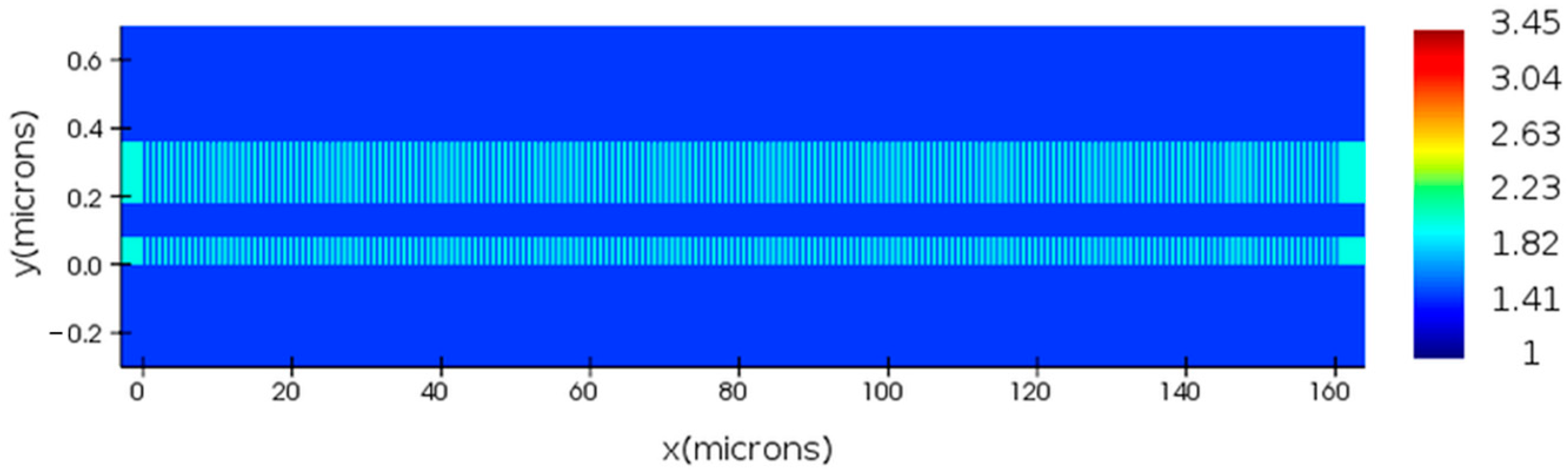
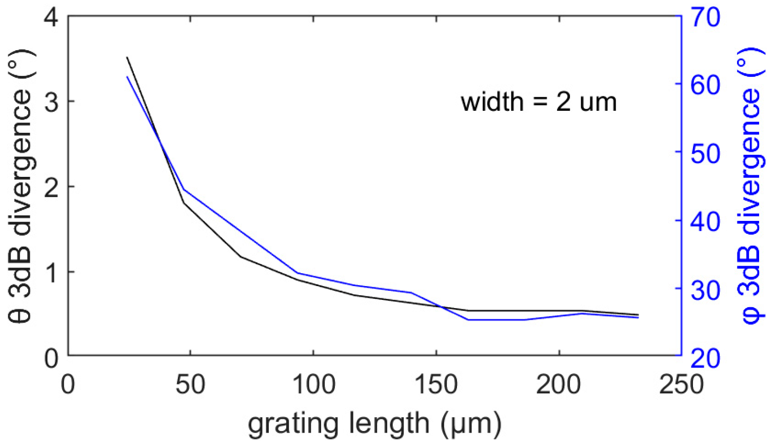
3.3. Non-Uniform Design

Due to the performance limitations of the uniform design, non-uniform configurations were also investigated to achieve more uniform emission profiles. The non-uniformity concerns the geometrical parameters of the design and suggests that along the grating length, some of the design parameters are being varied. Taking into account the fabrication process limitations and to ensure compatibility with Lionix TriPleX platform fabrication processes that enable only full etching, the parameters that can be varied are the waveguide width, the filling factor and the pitch.
The geometry variation of the non-uniform grating is designed to ensure a constant emission angle θ across the grating length for low θ angle divergence and increased resolution in the longitudinal axis. According to (1) and (2), to ensure a constant emission angle, the induced geometry variation needs to be designed carefully. In this study we varied the width and FF, keeping the pitch value constant and considering only fully etched waveguides. A top view and a sideview of the non-uniform design are shown in Figure 7 left and right, respectively. Moreover, the geometry variation targets uniform emission distributions. To achieve this, the k of every period should gradually increase across the grating length. Increasing k is achieved by decreasing the FF (approaching an FF of 0.5 that results in stronger emission) and increasing the width across the grating length, which leads to an increasing emission rate [27].
The design process started with FDE simulations using the Ansys Lumerical 2023 R2.3 MODE solver. First, the effective index of the fundamental TE mode of a waveguide cross section (n1), varying its width, is calculated given the ADS TriPleX layerstack. The results are shown in Figure 8. In the ADS TriPleX platform, to create the grating teeth, the Si3N4 is fully etched, removing both layers of the Si3N4 layerstack that are illustrated in Figure 2b. Therefore, the etched part of the grating geometry consists of SiO2. Since there is no waveguiding material in the etched part and the FDE solver cannot calculate any supported modes, we assumed the value of the effective refractive index of the etched part (n0) to be equal to the value of the refractive index of SiO2 (nSiO2). Using (1) and the calculated n1 values, it is then possible to compute the neff−grating for the different width and FF combinations. This is shown in Figure 9.
From the results shown in Figure 9, it is evident that for specific pairs of waveguide width and FF, the neff−grating remains constant. These contour lines, shown with black lines in Figure 9, are the desired regions from which the width–FF pairs can be extracted. The design methodology includes partitioning the available width range in N values to produce the width–FF pairs, as will be described shortly. Thus, it is ensured that the emission angle θ is also constant. Moreover, the emission profile of the grating is no longer exponential but becomes more uniform. This is achieved because across the grating length, the FF decreases toward 0.5, while the width increases, leading to an increasing k. For a given contour line, the corresponding coupling constant k has been calculated according to (3). Figure 10 illustrates k for three of the contour lines of Figure 9. It can be observed that for all the contour lines, k is similar, and it gradually increases as the width increases, according to the design target.
It is noted that there are multiple contour lines one can work with. A choice between the available options must therefore be made targeting optimal performance. In terms of keeping the emission angle constant, all the contour lines are equivalent. However, there are two more criteria that can help make the best choice.
The first one concerns the compatibility of the design with the fabrication process capabilities. The FF should remain below 0.9 for compatibility, with an acceptable minimum feature size of approximately 100 nm (for a pitch of around 1 μm, FF should be between 0.1 and 0.9). Moreover, the FF step should be as large as possible, leading to large steps in the grating tooth length and compatibility with the minimum step size. This is satisfied when choosing a contour line with a large slope in the whole width range. The same is true in the lateral direction, where large width steps are desirable for compatibility with a minimum step size. For a given GC length (fixed amount of GC periods and partitioning steps N), increasing the utilized width range will increase the width step. Note that we chose to work with a width larger than 1 μm for the proper confinement of the fundamental mode within the waveguide. Moreover, widths larger than 2 μm are not desirable since they impose limitations in the spacing between the array elements and full OPA size and also signify operation in the multimode regime.
A second criterion for choosing the contour line is the k value. Although between the different contour lines, the k values are similar, we see from Figure 10 that k shows a larger variation in the 1–1.5 μm width range, compared to the 1.5–2 width range. Therefore, there is a tradeoff between having a larger k variation and an acceptable width size. All things considered, the contour line that best fits all the criteria is marked with pink stars in Figure 9 and has neff−grating = 1.495.
After choosing the contour line, a polynomial fit is performed to extract the function that can then be used to calculate the width–FF pairs that will constitute the geometrical parameters of the design. To do this, the desired number of grating periods N is chosen. Then, N width values are sampled in the available width range, and according to the polynomial function, the corresponding FF values are computed. During this design study, we investigated multiple approaches with 1–1.5 μm and 1–2 μm width ranges and selected multiple contour line plots, both in the width range of 1–1.5 μm and in the width range of 1–2 μm, for comparison. The simulation results indicate that they all exhibit similar performance, and different designs were considered for fabrication to allow the experimental validation of their performance. In the rest of the paper, we show the results of a design with neff−grating = 1.495 and a width range of 1–2 μm.
Having defined the width–FF pairs, the rest of the geometrical parameters, namely, the pitch and the length (or, equivalently, the number of grating periods N) also need to be set. As with the uniform design, the pitch can be freely chosen according to the desired emission angle. It must be noted that at higher emission angles, the θ wavelength sensitivity is increased. This is due to Snell’s law at the air/SiO2 cladding interface. This was verified with simulations that showed a steering angle wavelength sensitivity of around 6°/100 nm for θ~0° and 11°/100 nm for θ~−40°. However, such large emission angles render the emitters difficult to operate on a system level, imposing strict requirements in terms of packaging. This results in a tradeoff between steering angle wavelength sensitivity and the complexity of packaging and system operation, and, depending on the application, the appropriate choice should be made. In this case, for an emission angle of −10°, a 926 nm pitch was calculated according to (2).
Concerning the number of grating periods N, this can also be freely chosen. Given the pitch, N will define the complete length of the grating (L), as L = pitch × N. However, a tradeoff also exists between the two parameters. On the one hand, gratings with a long length are needed for increased efficiency, long effective areas and small θ angle divergence. On the other hand, increasing the length (and therefore N) results in reducing the step size, both in the width and length dimensions. This happens because the width and FF pairs are limited both by the contour lines and the limited ranges—[1 μm–2 μm] and [0.1–0.9], respectively, as explained before. As a result, to have more periods, these ranges need to be partitioned into more parts, resulting in smaller step sizes. This threatens the GC fabricability with standard fabrication processes and might lead to misfabrications and degraded performance. To verify the effect of length variation on the performance of the grating, multiple 3D-FDTD simulations were performed keeping the rest of the parameters constant. The results are shown in Figure 11. We observe that, as the length increases, the θ and φ divergences decrease. For L = 93.52 μm (N = 100), the θ 3 dB divergence is 0.9°, and φ is 32.25°. For L = 186.13 μm (N = 200), the θ 3 dB divergence is 0.54°, and φ is 25.41°. For larger widths, the θ and φ divergences converge. This translates to a θ and φ divergence reduction of 87% and 57.4%, respectively, for the investigated length increase from 25 μm to 235 μm. The rest of the simulation results are produced for N = 200.
Having defined all the geometrical parameters of the GC, a 3D-FDTD simulation of the selected configuration was performed with the Ansys Lumerical 2023 R2.3 FDTD solver. Figure 12 illustrates the emission profile of the proposed non-uniform grating. It is observed that the emission profile is more uniform than the uniform design. Figure 13 shows the θ angle wavelength sensitivity for a pitch of 926 nm, revealing a steering angle of 7°/100 nm.

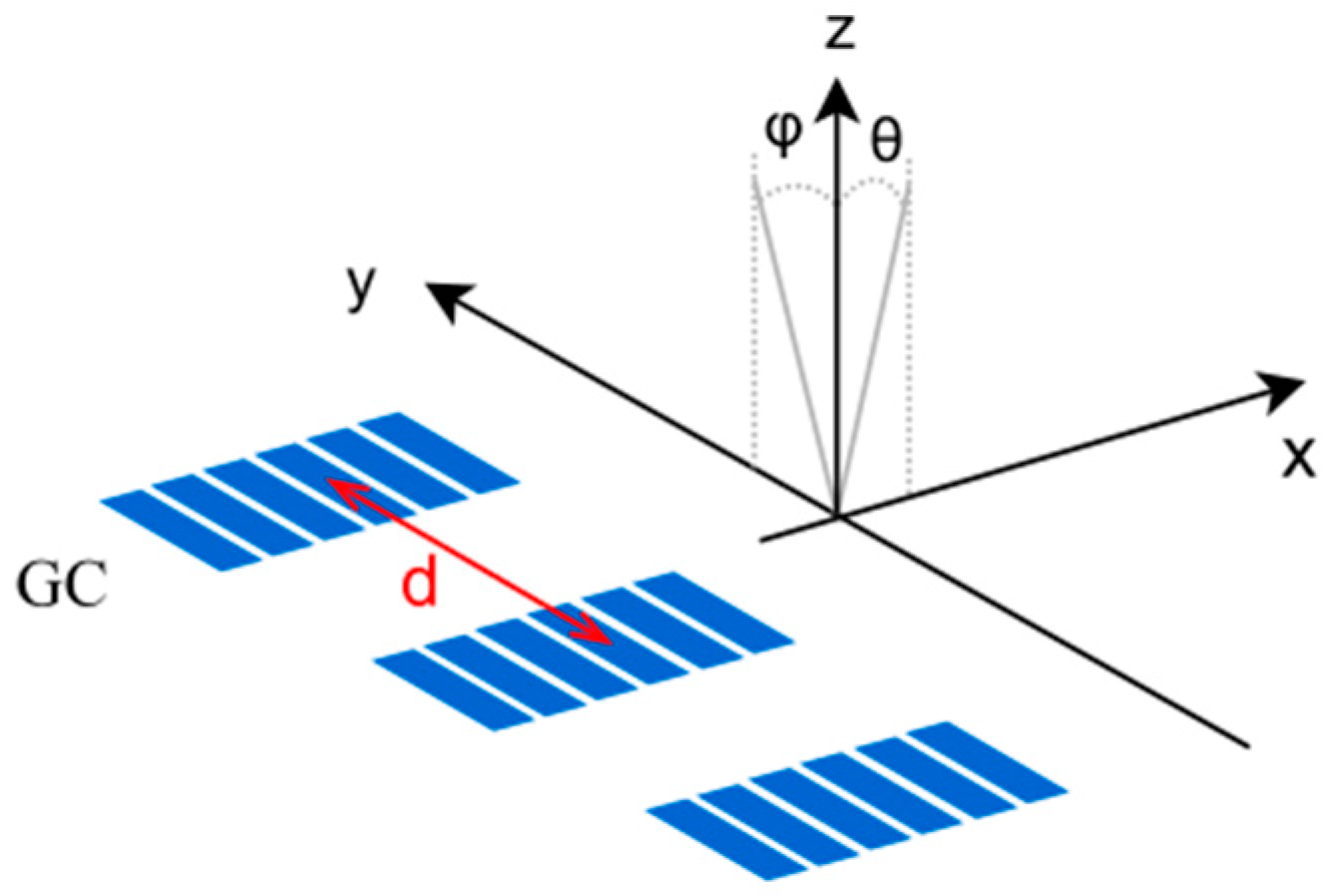
4. Design of the OPA Structure

After the design of the single radiator element was performed, we simulated the OPA structure and optimized its parameters, the number of elements in the antenna (NA) and their distance (d), defined as the center-to-center distance between two adjacent elements. This simulation was performed with the Sensor Array Analyzer toolbox by MATLAB R2024a, a toolbox that allows OPA structures and antennas to be created and simulated, extracting the radiation patterns and the θ and φ angle divergences.
More specifically, we varied NA between 2 and 8 and d between 1 and 2λ, where λ is the center wavelength and equals 1.55 μm. We investigated the variation profile of the values of directivity, the θ and φ angle divergences, while scaling the NA value.
We chose to work with NA up to 8; however, the design process is applicable to much higher NA values (e.g., 1024), only restricted by chip real-estate and packaging considerations. The resulting radiation plots are shown in Figure 14, given the radiation pattern of the selected non-uniform design of Figure 12. We can extract the θ angle divergence by examining the elevation cut of the directivity plots for an azimuthal angle equal to 0°. Such elevation cuts are shown in Figure 15 for two different OPA configurations. For the different antenna configurations of Figure 14, the θ 3 dB divergence is approximately 0.58°. This is illustrated in Figure 15, where the 3 dB region around the peak directivity value is marked with pink vertical arrows and the corresponding θ divergence is marked with horizontal red lines and equals 0.58°. This is in agreement with the results from the 3D-FDTD simulations, and it confirms that θ is not affected by ΝA, d, but rather depends on the design of the individual grating elements.
It is evident that a tradeoff exists between the number of side lobes, their peak directivities and the width of the main lobe, corresponding to the φ divergence. Depending on the application and whether emphasis needs to be given to either minimize the φ divergence or the number and size of the side lobes, an appropriate design choice can be made for NA and d.
Is it worth noting that there is another limiting factor for the distance d. This is the crosstalk between adjacent grating elements, which is affected by both the waveguide widths and their distance. If d is too small and the grating length is adequate for the power to couple from one grating to the other, there will be interference that will degrade the performance. To estimate this effect, FDE simulations were performed in which two waveguides were placed next to each other and the L10, which is the length required for 10% of the power to couple from waveguide 1 to waveguide 2, was calculated. This simulation was performed for different values of d and across the entire range of the investigated grating widths. The results are shown in Figure 16. To interpret the results, two things have to be considered that act simultaneously and affect the value of L10. On the one hand, for smaller widths, the same d (x-axis in Figure 16) means a bigger distance between the waveguides. At the same time, bigger widths mean better confinement of the mode in the waveguide, and therefore, smaller interactions between the adjacent waveguides. These two factors have opposite effects on the value of L10.
Overall, Table 1 summarizes the results extracted from Figure 16. The results indicate that for a distance d bigger than 2λ (3.1 μm), the L10 is larger than 200 μm; therefore, for shorter lengths, no crosstalk is expected. For spacing of 2.5λ (~3.8 μm), L10 is very large, so no crosstalk will appear in this case. For the proposed GC, which has lengths shorter than 200 μm, 2 and 2.5λ distances can be chosen. However, if the distance is only 1.5λ, then L10 is very low and below 50 μm. For OPAs with this d, some crosstalk between adjacent waveguides is expected. Therefore, although having a small d spacing between gratings, which minimizes unwanted sidelobes, might be preferred in some applications, 1 or 1.5λ spacing might not be feasible since it will lead to inevitable crosstalk between the adjacent waveguides, degrading the signal. This aspect must be taken into account when choosing the antenna parameters, depending always on the needs of every application.

5. Conclusions

In this study, we proposed a methodology that can be exploited for the design of flat emission PIC-based optical antennas. We applied this methodology to designing and optimizing a Si3N4 optical antenna based on ADS geometry, employing only full etching. The study focused first on optimizing the single radiator element, targeting a constant emission angle, low θ and φ angle divergences and a uniform emission profile. Both uniform and non-uniform geometries were investigated, showcasing θ and φ angle divergences of 0.9° and 32° and 0.54° and 25.41°, respectively. Also, a wavelength sensitivity of 7°/100 nm was achieved. Lastly, the OPA structure was optimized, and the effect of the NA and d parameters was investigated. For eight elements in the OPA, we achieved 35 dBi of peak directivity.

Author Contributions

Conceptualization, T.P., G.P., G.S. and C.Z.; methodology, T.P., G.P., R.B. and C.Z.; software, T.P. and G.P.; investigation, T.P. and G.P.; resources, T.P., G.P. and D.A.; data curation, T.P., G.P. and C.Z.; writing—original draft preparation, T.P.; writing—review and editing, T.P., G.P., G.S., E.K., C.Z. and D.A.; visualization, T.P.; supervision, D.A. All authors have read and agreed to the published version of the manuscript.

Funding

This work has received funding from the European Union’s Horizon Europe initiative, programme HORIZON-CL4-2022-DIGITAL-EMERGING-01-03, under grant agreement No. 101093013 (PARALIA).

Institutional Review Board Statement

Not applicable.

Informed Consent Statement

Not applicable.

Data Availability Statement

The original contributions presented in this study are included in the article. Further inquiries can be directed to the corresponding author(s).

Conflicts of Interest

The authors declare no conflict of interest.

Abbreviations

The following abbreviations are used in this manuscript:
LidarLight detection and ranging
PICPhotonic integrated circuit
OPAOptical phased array
UAMAutomated urban air mobility
RadarRadio detection and ranging
3DThree-dimensional
FOVField of view
MEMSMicro-electromechanical system
SOISilicon on insulator
CMOSComplementary metal-oxide semiconductor
1DOne-dimensional
2DTwo-dimensional
Si3N4Silicon nitride
ADSAsymmetric double stripe
MPWMulti-project wafer
GCGrating coupler
SiO2Silicon dioxide
neffEffective refractive index
FDEFinite-difference eigenmode
FDTDFinite-difference time domain
FFFilling factor

References

  1. Ahmed, F.; Mohanta, J.C.; Keshari, A.; Yadav, P.S. Recent Advances in Unmanned Aerial Vehicles: A Review. Arab. J. Sci. Eng. 2022, 47, 7963–7984. [Google Scholar] [CrossRef]
  2. Bathla, G.; Bhadane, K.; Singh, R.K.; Kumar, R.; Aluvalu, R.; Krishnamurthi, R.; Kumar, A.; Thakur, R.N.; Basheer, S. Autonomous Vehicles and Intelligent Automation: Applications, Challenges, and Opportunities. Mob. Inf. Syst. 2022, 2022, 7632892. [Google Scholar] [CrossRef]
  3. Ayala, R.; Mohd, T.K. Sensors in Autonomous Vehicles: A Survey. J. Auton. Veh. Syst. 2021, 1, 031003. [Google Scholar] [CrossRef]
  4. Falconi, F.; Melo, S.; Scotti, F.; Malik, M.N.; Scaffardi, M.; Porzi, C.; Ansalone, L.; Ghelfi, P.; Bogoni, A. A Combined Radar & Lidar System Based on Integrated Photonics in Silicon-on-Insulator. J. Light. Technol. 2021, 39, 17–23. [Google Scholar] [CrossRef]
  5. Xu, Z.; Zhao, J.; Zhang, F.; Zhang, L.; Yang, T.; Li, Q.; Pan, S. Photonics-Based Radar-Lidar Integrated System for Multi-Sensor Fusion Applications. IEEE Sens. J. 2020, 20, 15068–15074. [Google Scholar] [CrossRef]
  6. Li, Y.; Ibanez-Guzman, J. Lidar for Autonomous Driving: The Principles, Challenges, and Trends for Automotive Lidar and Perception Systems. IEEE Signal Process. Mag. 2020, 37, 50–61. [Google Scholar] [CrossRef]
  7. Royo, S.; Ballesta-Garcia, M. An Overview of Lidar Imaging Systems for Autonomous Vehicles. Appl. Sci. 2019, 9, 4093. [Google Scholar] [CrossRef]
  8. Holzhüter, H.; Bödewadt, J.; Bayesteh, S.; Aschinger, A.; Blume, H. Technical concepts of automotive LiDAR sensors: A review. Opt. Eng. 2023, 62, 031213. [Google Scholar] [CrossRef]
  9. Raj, T.; Hashim, F.H.; Huddin, A.B.; Ibrahim, M.F.; Hussain, A. A Survey on LiDAR Scanning Mechanisms. Electronics 2020, 9, 741. [Google Scholar] [CrossRef]
  10. Hu, M.; Pang, Y.; Gao, L. Advances in Silicon-Based Integrated Lidar. Sensors 2023, 23, 5920. [Google Scholar] [CrossRef]
  11. Li, N.; Ho, C.P.; Xue, J.; Lim, L.W.; Chen, G.; Fu, Y.H.; Lee, L.Y.T. A Progress Review on Solid-State LiDAR and Nanophotonics-Based LiDAR Sensors. Laser Photonics Rev. 2022, 16, 2100511. [Google Scholar] [CrossRef]
  12. Poulton, C.V.; Byrd, M.J.; Russo, P.; Timurdogan, E.; Khandaker, M.; Vermeulen, D.; Watts, M.R. Long-Range LiDAR and Free-Space Data Communication with High-Performance Optical Phased Arrays. IEEE J. Sel. Top. Quantum Electron. 2019, 25, 7700108. [Google Scholar] [CrossRef]
  13. Hashemi, H. A Review of Silicon Photonics LiDAR. In Proceedings of the 2022 IEEE Custom Integrated Circuits Conference (CICC), Newport Beach, CA, USA, 24–27 April 2022; pp. 1–8. [Google Scholar]
  14. Yoon, J.; Yoon, H.; Kim, J.-Y.; Kim, J.; Kang, G.; Kwon, N.-H.; Kurt, H.; Park, H.-H. Demonstration of high-accuracy 3D imaging using a Si optical phased array with a tunable radiator. Opt. Express 2023, 31, 9935. [Google Scholar] [CrossRef] [PubMed]
  15. Ren, W.; Liang, Q.; Feng, J.; Liu, H.; Hu, J.; Yuan, S.; Xia, X.; Jiang, W.; Zhan, Q.; Zeng, H. Free-space beam shaping and steering based on a silicon optical phased array. Photonics Res. 2023, 11, 2093. [Google Scholar] [CrossRef]
  16. Heck, M.J.R. Highly integrated optical phased arrays: Photonic integrated circuits for optical beam shaping and beam steering. Nanophotonics 2017, 6, 93–107. [Google Scholar] [CrossRef]
  17. Han, X.; Wang, Q.; Wang, Z.; Fang, Y.; He, Y.; Geng, W.; Pan, Z.; Yue, Y. Solid-State Photonics-Based Lidar with Large Beam-Steering Angle by Seamlessly Merging Two Orthogonally Polarized Beams. IEEE J. Sel. Top. Quantum Electron. 2021, 27, 8300608. [Google Scholar] [CrossRef]
  18. Van Acoleyen, K.; Bogaerts, W.; Baets, R. Two-Dimensional Dispersive Off-Chip Beam Scanner Fabricated on Silicon-On-Insulator. IEEE Photonics Technol. Lett. 2011, 23, 1270–1272. [Google Scholar] [CrossRef]
  19. Im, C.-S.; Bhandari, B.; Lee, K.-P.; Kim, S.-M.; Oh, M.-C.; Lee, S.-S. Silicon nitride optical phased array based on a grating antenna enabling wavelength-tuned beam steering. Opt. Express 2020, 28, 3270. [Google Scholar] [CrossRef]
  20. Xu, W.; Guo, Y.; Li, X.; Liu, C.; Lu, L.; Chen, J.; Zhou, L. Fully Integrated Solid-State LiDAR Transmitter on a Multi-Layer Silicon-Nitride-on-Silicon Photonic Platform. J. Light. Technol. 2023, 41, 832–840. [Google Scholar] [CrossRef]
  21. Malhouitre, S.; Fowler, D.; Garcia, S.; Lemonnier, O.; Tyler, N.; Rabaud, W. Silicon Nitride Photonic Platform for LIDAR Applications. In Proceedings of the 2018 IEEE 15th International Conference on Group IV Photonics (GFP), Cancun, Mexico, 29–31 August 2018; pp. 1–2. [Google Scholar]
  22. Wang, Q.; Wang, S.; Jia, L.; Cai, Y.; Yue, W.; Yu, M. Silicon nitride assisted 1×64 optical phased array based on a SOI platform. Opt. Express 2021, 29, 10509. [Google Scholar] [CrossRef]
  23. Poulton, C.V.; Byrd, M.J.; Raval, M.; Su, Z.; Li, N.; Timurdogan, E.; Coolbaugh, D.; Vermeulen, D.; Watts, M.R. Large-scale silicon nitride nanophotonic phased arrays at infrared and visible wavelengths. Opt. Lett. 2017, 42, 21. [Google Scholar] [CrossRef]
  24. Wörhoff, K.; Heideman, R.G.; Leinse, A.; Hoekman, M. TriPleX: A versatile dielectric photonic platform. Adv. Opt. Technol. 2015, 4, 189–207. [Google Scholar] [CrossRef]
  25. Roeloffzen, C.G.H.; Hoekman, M.; Klein, E.J.; Wevers, L.S.; Timens, R.B.; Marchenko, D.; Geskus, D.; Dekker, R.; Alippi, A.; Grootjans, R.; et al. Low-Loss Si3N4 TriPleX Optical Waveguides: Technology and Applications Overview. IEEE J. Sel. Top. Quantum Electron. 2018, 24, 4400321. [Google Scholar] [CrossRef]
  26. Raval, M.; Poulton, C.V.; Watts, M.R. Unidirectional waveguide grating antennas with uniform emission for optical phased arrays. Opt. Lett. 2017, 42, 2563. [Google Scholar] [CrossRef]
  27. Shang, K.; Qin, C.; Zhang, Y.; Liu, G.; Xiao, X.; Feng, S.; Yoo, S.J.B. Uniform emission, constant wavevector silicon grating surface emitter for beam steering with ultra-sharp instantaneous field-of-view. Opt. Express 2017, 25, 19655. [Google Scholar] [CrossRef] [PubMed]
  28. Yepez, P.A.K.; Scholz, U.; Zimmermann, A. Temperature Dependence of the Steering Angles of a Silicon Photonic Optical Phased Array. IEEE Photonics J. 2020, 12, 6800813. [Google Scholar] [CrossRef]
  29. Spencer, D.T.; Davenport, M.; Srinivasan, S.; Khurgin, J.; Morton, P.A.; Bowers, J.E. Low kappa, narrow bandwidth Si_3N_4 Bragg gratings. Opt. Express 2015, 23, 30329. [Google Scholar] [CrossRef] [PubMed]
Figure 1. Schematic of an optical antenna in OPA configuration based on grating couplers. The θ and φ angles and the distance d between adjacent GC elements are noted.
Photonics 12 00214 g001
Figure 2. (a) The OPA schematic to indicate the cross-sectional planes. (b) Schematic of the yz-plane cross section of the standard TriPleX ADS waveguide. The different regions (Si3N4 waveguide, SiO2 top oxide layer (TOX) and bottom oxide layer (BOX) and air top cladding) are marked with different colors. (c) Schematic of the sideview (xz-plane cross section) of a periodic grating structure. The grating pitch is denoted with Λ and the filling factor with FF. The effective index of the etched part is n0 and of the unetched part is n1.
Photonics 12 00214 g002
Figure 3. Sideview of the uniform GC, showing the constant pitch, FF and width across the direction of propagation.
Photonics 12 00214 g003
Figure 4. Simulated θ and φ angle divergences, (a) varying the grating width for a fixed length of 50 μm and (b) varying the grating length for a fixed width of 2 μm.
Photonics 12 00214 g004
Figure 5. (Left): Top view of the emission profile of the uniform grating for a width of 2 μm and a length of 100 μm. The Ez component field distribution is shown with a color scale. (Right): A 1D plot of the emission profile along the dashed line of the left figure.
Photonics 12 00214 g005
Figure 6. Calculated emission angle θ of the far-field profile, varying the wavelength in the range of 1.5–1.6 μm for a uniform tooth profile and a pitch of 926 nm. The electric field intensity is shown with a color scale.
Photonics 12 00214 g006
Figure 7. (Left) Top view and (Right) sideview of the investigated non-uniform grating design with a varying width and FF.
Photonics 12 00214 g007
Figure 8. Calculated effective refractive index of the TE0 mode varying the waveguide width.
Photonics 12 00214 g008
Figure 9. neff−grating of the fundamental supported mode calculated via FDE simulations, varying the waveguide width and FF. The black lines are the contour lines of the plots along which the neff−grating has a constant value. The selected contour line is marked with pink stars.
Photonics 12 00214 g009
Figure 10. The calculated coupling constant k for the different width values across the grating for three of the contour lines.
Photonics 12 00214 g010
Figure 11. Simulated θ and φ angle divergences varying the grating length for width–FF pairs calculated from the same contour line.
Photonics 12 00214 g011
Figure 12. (Left): Top view of the emission profile of the non-uniform grating for the selected geometrical parameters. The Ez component field distribution is shown with a color scale. (Right): A 1D plot of the emission profile along the dashed line of the left figure.
Photonics 12 00214 g012
Figure 13. Calculated emission angle θ of the far-field profile, varying the wavelength in the range of 1.5–1.6 μm, for the non-uniform tooth profile and a pitch of 926 nm. The electric field intensity is shown with a color scale.
Photonics 12 00214 g013
Figure 14. 3D directivity plots (in dBi) produced with the Sensor Array Analyzer app, varying the number (NA) of grating elements and the distance (d) between them. The axis information is mentioned in the first subplot and is the same for all the subplots. The colorbar shows the directivity in dBi.
Photonics 12 00214 g014
Figure 15. Elevation cut for azimuth angle = 0° for two of the directivity plots of Figure 14. On the other hand, the divergence of the φ angle is affected by the OPA topology, both by the number of elements NA and by their distance d. Increasing the NA reduces the φ divergence of the main lobe. Also, increasing the distance between adjacent elements reduces the main lobe φ divergence. It can also be seen in Figure 14 that increasing the number of elements (for a fixed distance) will result in the appearance of more side lobes with lower peak directivities, while the width of the main lobe is reduced. A similar effect is observed when the number of elements is kept constant and their distance is increased. In this case, more side lobes appear, and their peak directivity is also increased. Lastly, from the directivity plots, the peak directivity value can be extracted. This is 34.8 dBi for NA = 4 and d = 1.5λ and 35 dBi for NA = 8 and d = 1.5λ.
Photonics 12 00214 g015
Figure 16. Calculated L10 varying the distance d between two adjacent waveguides, with widths of 1 μm, 1.5 μm and 2 μm.
Photonics 12 00214 g016
Table 1. Calculated L10 for the different width and distance combinations, as extracted from Figure 16.
d1.5λ2λ2.5λ
Width
1 μm45 μm250 μm1400 μm
1.5 μm40 μm300 μm2280 μm
2 μm20 μm185 μm1600 μm
Disclaimer/Publisher’s Note: The statements, opinions and data contained in all publications are solely those of the individual author(s) and contributor(s) and not of MDPI and/or the editor(s). MDPI and/or the editor(s) disclaim responsibility for any injury to people or property resulting from any ideas, methods, instructions or products referred to in the content.

