Article

Structure-Optimized Photonic Phase-Change Memory Achieving High Storage Density and Endurance Towards Reconfigurable Telecommunication Systems

by
Chen Gao
1,2,*,†,
Zhou Han
1,2,†,
Gaofei Wang
1,2 and
Wentao Huang
1,2
1
College of Integrated Circuits & Micro-Nano Electronics, Fudan University, Shanghai 200433, China
2
Shaoxin Laboratory, Shaoxing 312000, China
*
Author to whom correspondence should be addressed.
These authors contributed equally to this work.
Photonics 2025, 12(11), 1130; https://doi.org/10.3390/photonics12111130 (registering DOI)
Submission received: 21 October 2025 / Revised: 1 November 2025 / Accepted: 14 November 2025 / Published: 15 November 2025

Abstract

Next-generation photonic memory, leveraging broad spectral operability and electromagnetic immunity, enables ultrafast data storage with high density, overcoming the physical limitations of silicon-based electronic memory in the post-Moore era. Phase-change materials (PCMs) are particularly promising for photonic memory due to their exceptional optical contrast between amorphous and crystalline states. Furthermore, photonic phase-change memory can be deployed as tunable components (such as optical attenuators and delay lines) within reconfigurable integrated photonic systems for telecommunications and computing. Here, we optimize the thickness of PCM cells to maximize crystalline-state light absorption and enhance transmission contrast. The resulting photonic memory achieves outstanding performance: ultralow-energy programming (0.96 pJ/operation), 9 fJ detection sensitivity, >105 s retention, 6000-cycle endurance, and multi-level storage capacity (209 distinct states). Furthermore, by structuring the PCM into a micro-cylinder array atop a PCM film, we achieve stable transmission contrast through 2 × 10⁶ cycles—far exceeding the durability of single-cell structures—and an 8.69 dB improvement in contrast over film-free micro-cylinder arrays. These advances highlight the critical role of microstructural optimization in enabling high-performance, on-chip photonic memory for future integrated photonic telecommunication and computing systems.

1. Introduction

Driven by exponential data growth and rapid artificial intelligence (AI) advancement, next-generation memory demands higher speed [1,2], lower energy consumption [3,4], extended retention [5], and improved endurance [5,6]. State-of-the-art electronic memory, however, faces fundamental barriers, including quantum tunneling [7], dielectric leakage currents [8,9], and thermal runaway in 3D integration—ultimately limiting further scaling and performance gains. Optical memory emerges as a promising solution, leveraging its broad spectral range and inherent wavelength-division multiplexing (WDM) to enable massively parallel architectures, ultrahigh bandwidth, ultralow latency, and intrinsic electromagnetic interference immunity [10,11]. This positions optical memory as a critical alternative to silicon-based electronic memory in the post-Moore era.
Phase-change materials (PCMs) enable direct optical modulation through pronounced refractive index n [12,13] and extinction coefficient k [14] contrasts between different states, permitting dynamic control of light’s intensity and phase. This inherent optoelectronic switching capability positions photonic phase-change memory as a leading contender for non-volatile optical storage. Despite both electronic and photonic phase-change memory operating on the same fundamental principle of material phase transition, they exhibit significant performance differences, particularly in scalability, switching energy, and integration potential. Electronic phase-change memory faces considerable challenges in scaling. High current densities and Joule heating effects exacerbate electromigration and thermal crosstalk issues at advanced technology nodes. Moreover, its switching energy efficiency is inherently limited by the electro-thermal conversion process. In contrast, photonic phase-change memory offers inherent scalability, as its operation relies on optical field confinement rather than current injection, thereby bypassing the limitations of metal interconnects. It enables direct phase transition via optical pulses, eliminating energy losses from contact resistance and unwanted Joule heating in non-target regions, which significantly reduces switching energy. The combination of wavelength-division multiplexing (WDM) technology and the high bandwidth characteristic of photonic phase-change memory supports massively parallel multi-channel data processing and access. Furthermore, its native compatibility with mature photonic integration platforms such as silicon photonics provides a clear pathway for wafer-scale high-density integration with conventional electronic components.
Based on the physical mechanisms, PCMs for photonic memory can be classified into two categories: intensity-modulation PCMs and phase-modulation PCMs. Intensity-modulation PCMs exhibit a significant difference in extinction coefficient (Δk) between their different phases, and phase transition is induced by optical pulses or electrical heaters. The most typical examples are PCMs with Ge-Sb-Te compounds. The seminal 2015 demonstration of on-chip photonic phase-change memory used waveguide-integrated Ge2Sb2Te5 (GST) cells [15]. Recent advances in novel PCMs have since achieved orders-of-magnitude improvements in critical metrics for photonic memory: read/write speeds [16,17] and endurance [18]. Among these, Sb-based fast-acting PCMs offer higher switching speeds and lower energy consumption. Sb-based photonic memory achieves optical switching with 800 fs pulses [16] and sub 100 pJ programming energy (as low as 59 pJ) [16]. In contrast, phase-modulation PCMs are typically low-loss materials with a large refractive index contrast (Δn) between phases, such as Sb2Se3 and Sb2S3. They are generally switched using electrical heaters and exhibit superior endurance. For example, a Mach-Zehnder interferometer (MZI) integrated with a single Sb2Se3 patch can endure at least 3000 switching cycles [18]. Furthermore, both the geometric design of the electrical heater [19] and the array configuration of PCMs [20] can contribute to effective thermal budget optimization. The monolithic back-end-of-line integration of PCMs into foundry-manufactured silicon photonics [21] demonstrates the potential for further compatibility with CMOS technology. Notably, structural optimization of PCM cells provides a critical pathway for performance enhancement. Nanodisk-transformed GST arrays on ring resonators boost transmission contrast from 5 dB to 21.3 dB [22]. Tapered GST island arrays enable 64-level optical mode conversion through graded width modulation [23]. For Sb2Se3 sub-cell arrays on MZI arms, 105 operational cycles are achieved while maintaining substantial amorphous-crystalline contrast—tripling the endurance of single-cell configurations [18]. These geometric innovations enhance transmission metrics while promoting uniform thermal distribution for reliability [20].
Furthermore, due to the non-volatile programmability of photonic phase-change memory, its applications can be extended to reconfigurable tunable photonic components. The significant optical contrast between different states of photonic phase-change memory enables effective modulation of optical signals, making it suitable for components such as optical attenuators [24], optical switches [25], and optical delay lines [26]. Additionally, the nanoscale patterning of PCMs can achieve complex functions like mode conversion [23,27] and signal routing [28]. Therefore, optimizing the performance of photonic phase-change memory contributes to the enhanced reconfigurability and comprehensive advancement of integrated photonic telecommunication and computing systems in the fields of data storage, dynamic data processing, and signal routing.
Here, we pioneer vertical height (thickness) and nanopattern array engineering in photonic PCM cells, achieving simultaneous enhancement of storage density and cycling stability—addressing critical scaling challenges in phase-change photonics. Vertical height optimization maximizes resonant absorption in crystalline states while enabling maximum transmission contrast for photonic memory. Experimentally, this yields ultralow programming energy (0.96 pJ), high endurance (>6000 cycles), and multilevel capacity (209 distinguishable states), with superior retention and fJ read energy. On the other hand, micro-cylinder arrays engineered on PCM films achieve >2 × 10⁶ cycle endurance—outperforming single cells—while optimally balancing transmission contrast and stability. This structural design strategy resolves the endurance-contrast trade-off, enabling high-performance photonic memory for scalable photonic integrated circuits.

2. Materials and Methods

Photonic memory device fabrication. Photonic memory devices were fabricated on a Si3N4 platform comprising a 340 nm Si3N4 layer and a 2 μm silicon dioxide (SiO2) film on a silicon wafer. Electron beam lithography (JEOL 8100, JEOL Ltd., Akishima, Tokyo, Japan) was employed to define the photonic waveguide structures, with a 450 nm layer of ZEP520-A (ZEON CORPORATION, Tokyo, Japan) positive resist spin-coated on the wafer. The patterning was followed by etching 160 nm of Si3N4 using an inductively coupled plasma etcher (PlasmaPro 100, Oxford Instruments, High Wycombe, UK) with a CHF3/O2 gas mixture. After that, an atomic layer deposition (ALD) process (MNT-S, MNT, Wuxi, China) at 250 °C was used to deposit a 10 nm Al2O3 layer as an etch-stop layer. A second lithographic step, using a poly(methyl methacrylate) (PMMA, Allresist, Strausberg, Germany) resist, defined the germanium-antimony-telluride (GST) pattern. GST (50 nm) was subsequently deposited using physical vapor deposition (PVD 75, kurt J Lesker, Jefferson Hills, PA, USA). A third electron beam lithography (EBL) step defined the nano-structured array on the waveguide, followed by a 40 nm etch in a reactive ion etcher (Si 591, Sentech, Krailling, Germany). The GST structures were then encapsulated by a 50 nm Al2O3 layer, deposited via ALD at 150 °C.
Optical simulation. Optical simulations were performed using the finite-difference time-domain (FDTD) method with Lumerical FDTD Solutions (Ansys Lumerical 2024 R2). The refractive index of GST was measured using an ellipsometer (UVISEL Plus, Horiba, Sunnyvale, CA, USA). A 1550 nm laser operating in the fundamental TE mode is used to analyze the optical field distribution. The optical input power is set at 0.5 mW. The mode source exhibits a TE polarization fraction of 99.08%, while the waveguide TE/TM fraction is 91.74%/84.37%. All boundaries of the simulation domain are configured as Perfectly Matched Layers (PML).
Optical transmission measurement. To monitor the switching of the photonic memory device in situ, optical transmission was measured using pump and probe signals of different wavelengths. The optical transmission measurement system is shown in Figure S1 of the Supplementary Materials. The probe signal was provided by a continuous-wave (CW) diode laser (TSL-570, Santec, Komaki City, Japan) with a power of 0.5 mW, and its transmission through the photonic memory device was recorded by a photodetector (2011-FC-M, Newport, San Jose, CA, USA). The high-power pump signal was generated by another diode laser (N7714A, Keysight, Santa Rosa, CA, USA), modulated by an electro-optic modulator (EOM, Lucent, Murray Hill, NJ, USA), and controlled by an arbitrary waveform generator (31102A/81160A, Tektronix, Los Angeles, CA, USA/Keysight). The pump signal was amplified using an optical fiber amplifier (AEDFA-C-EX-DWDM-27, Amonics, Hong Kong, China). To suppress interference between the pump and probe signals, an optical bandpass filter (OTF930, Santec, Komaki City, Japan) was placed in the optical path before the pump/probe route.

3. Thickness Design of Photonic Phase-Change Memory

We fabricated photonic phase-change memory cells with varying GST thicknesses (H), where devices comprise 3-μm-thick SiO2 substrates supporting 340 nm Si3N4 ridge waveguides (total height: 0.34 μm, ridge size: 0.16 μm height × 1.3 μm width), with GST cells positioned above the waveguides along a 3-μm optical propagation path and encapsulated with a 100 nm SiO2 cladding layer, as shown in Figure 1a,b. To validate GST’s phase transformation capability, 50 nm GST was deposited on silicon substrates by magnetron sputtering at a power of 30 W. This was immediately followed by a protective 20 nm ITO layer deposited under identical sputtering conditions (30 W). Figure 1c presents XRD patterns of air-annealed GST films, where as-deposited samples and samples annealed at 100 °C exhibit amorphous characteristics. Annealing at 150 °C induces a prominent F(200) peak, confirming transition to a metastable cubic crystalline phase. At elevated temperatures (200–300 °C), peak shifting occurs with the emergence of the H(013) plane diffraction, verifying full transformation to the thermodynamically stable hexagonal phase. Spectroscopic ellipsometry measurements (Figure 1d) quantify the optical contrast between as-deposited amorphous GST (aGST) and annealed hexagonal-phase crystalline GST (cGST). At 1550 nm wavelength, cGST exhibits significantly enhanced optical constants (n = 5.59, k = 0.71) versus aGST (n = 4.38, k = 0.09), confirming substantial refractive index elevation (Δn = 1.21) and absorption increase (8-fold k increase) upon crystallization.
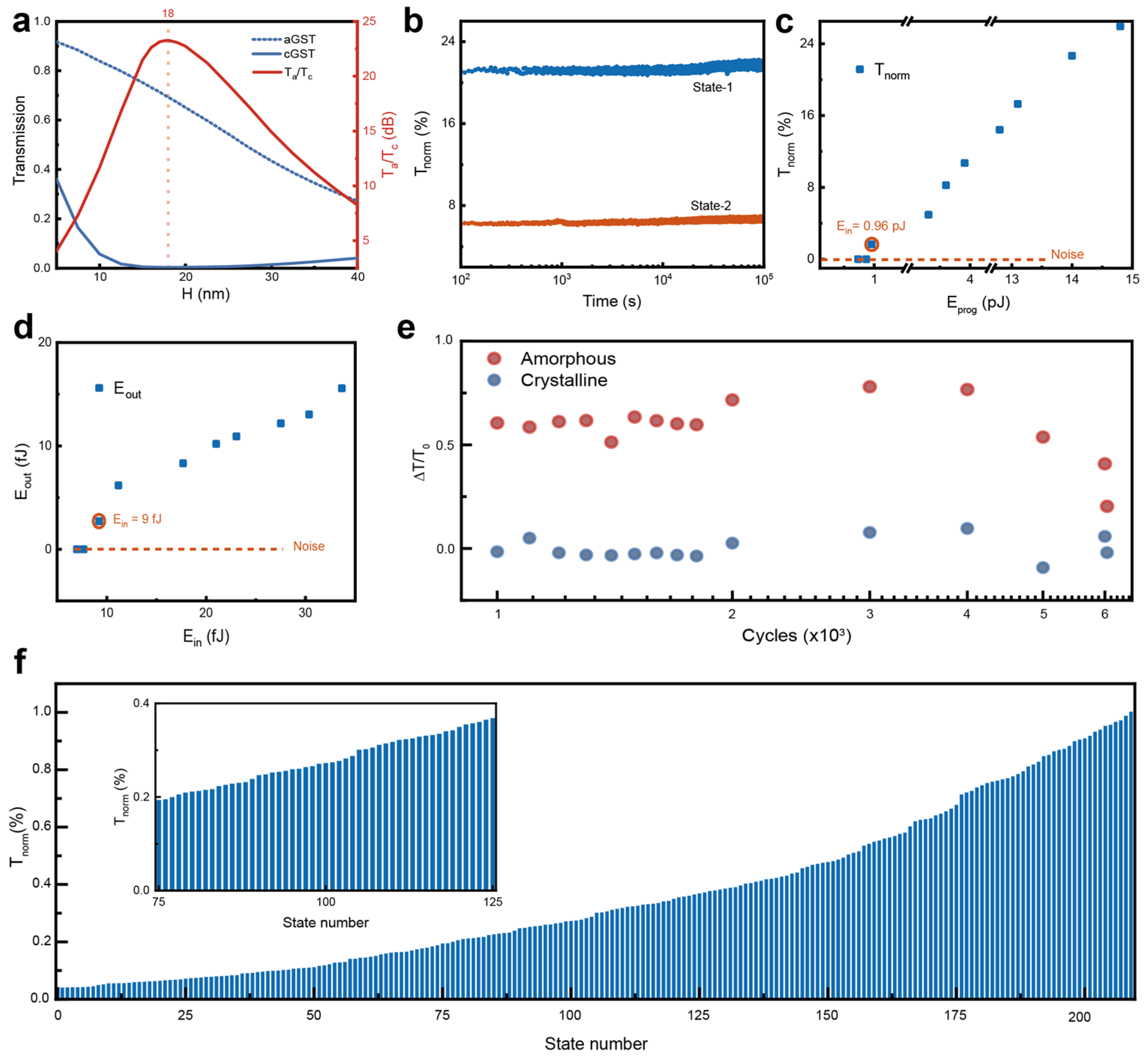
To maximize storage density, we systematically investigated transmission contrast in photonic phase-change memory cells by varying the critical dimension H using finite-difference time-domain (FDTD) simulations (Lumerical DEVICE Suite, Ansys Lumerical 2024 R2). Both read and write operations were modeled using 1550 nm fundamental TE-mode optical pulses to induce a probe phase transition. Figure 2a reveals distinct transmission trends versus critical dimension H: aGST cells exhibit monotonically decreasing transmission (Ta), while cGST cells show non-monotonic transmission behavior (Tc) with an initial reduction followed by recovery. The maximum transmission ratio Ta/Tc = 23.28 dB occurs at H = 18 nm. The optical mode profiles of the photonic phase-change memory at H = 18 nm in both crystalline and amorphous states are shown in Figure S2 of the Supplementary Materials. As demonstrated, no mode leakage is observed in either state, and the optical field strongly interacts with the PCM. This confirms the excellent optical confinement and efficient light-matter interaction in our device. This optimum geometry was consequently selected for experimental validation of photonic phase-change memory performance. Optical programming in Figure 2b demonstrates non-volatile switching between two bistable states: State-1 (high-transmission) and State-2 (low-transmission). Both states exhibit exceptional stability with transmittance retention exceeding 105 s, confirming robust non-volatile capability. To further verify the device performance after the retention characteristics test, the switching stability before and after the retention test under identical programming pulse cycling conditions was tested in Figure S3 of the Supplementary Materials. The device exhibited highly consistent transmission profiles, demonstrating three stable switching cycles between low- and high-transmission states with only minor transmission fluctuations in both states. These results confirm that the device performance remains unchanged after the retention characteristics test. Figure 2c shows ultralow-power switching characteristics, where a 0.96 pJ programming pulse triggers a discernible increase in the transmission level. To strengthen the credibility of the ultralow programming energy of 0.96 pJ, the transmission modulation characteristics of four additional devices were tested in Figure S4 of the Supplementary Materials. All tested devices exhibited minimum programming energies below 0.96 pJ, conclusively verifying the ultralow energy operation of the photonic phase-change memory. This exceptional energy efficiency originates from the geometry-optimized GST cell operating at maximum crystallization/amorphous contrast, leveraging enhanced optical absorption of cGST. The achieved programming energy represents a record-low value for photonic phase-change memories, demonstrating critical progress toward practical photonic computing systems. Detection sensitivity characterization in Figure 2d reveals sub-10 fJ optical read capability, where 9 fJ probe pulses generate measurable output signals in the minimum transmission state. While geometry optimization theoretically increases insertion loss, the experimentally achieved minimum transmission state exhibits incomplete crystallization, reducing actual losses significantly lower than simulations. This unanticipated partial crystallinity enables sufficient detection sensitivity despite theoretical constraints. The cycling endurance was tested in Figure 2e. Between 1000 and 2000 cycles, the average crystalline transmission (T0) and amorphous transmission (T1) were acquired and calculated every 100 cycles from 20 consecutive switching cycles, and the relative transmission contrast ∆T/T0 = (T1T0)/T0 was derived. Beyond 2000 cycles up to 6000 cycles, the same averaging procedure was performed every 1000 cycles. The cycling endurance test confirms robust bistable operation through 6000 reversible phase transitions at the maximum transmission contrast, with both crystalline and amorphous states maintaining distinct transmission bands and no observable overlap. Both crystalline and amorphous transmission exhibited only minor fluctuations during the 1000–2000 and 2000–4000 cycle intervals, demonstrating excellent cycling stability of the photonic phase-change memory. And the sudden change in transmission contrast around 2000 cycles is likely attributable to a slight system offset introduced by the adjustment in the measurement method. The thickness-optimized structure sustains good endurance, although the amorphous state exhibits observable transmission degradation after 4000 cycles. Figure 2f showcases continuous multilevel programmability through progressive pulse-energy modulation, achieving 209 distinguishable states that establish a record capacity density (>7.6 bits) for integrated nonvolatile photonic memories. The inset of Figure 2f provides a more intuitive and clear demonstration of the complete absence of transmission overlap between all adjacent states, thereby confirming the distinguishable characteristics of each programmed state in the photonic phase-change memory. The excellent multi-level storage capability enhances data throughput and reduces the device footprint, thereby enabling large-scale high-precision optical computing and signal processing. Improvement in multi-level storage capability supports advanced applications such as high-dimensional data encoding and synaptic weight simulation. This breakthrough analog control exploits the engineered transmission contrast enabled by height-optimized resonance enhancement.

4. Photonic Phase-Change Memory Based on Nanopattern Array

To enhance device endurance and local optical field confinement, we engineered periodic nanopatterned GST arrays (Figure 3) as a dual-function alternative to conventional uniform PCM films. These subwavelength geometries provide physical reinforcement against interfacial delamination and thermomechanical fatigue through stress distribution across unit cells, thereby extending cycling lifetimes > 300× versus planar counterparts. Concurrently, the nanostructuring enables diffraction-limited optical modulation via resonant near-field enhancement, achieving spatially localized phase transitions critical for massively scalable, dynamically reconfigurable photonic circuits. Figure 3 presents a comprehensive 3D FDTD analysis of micro-cylinder GST arrays integrated on Si3N4 waveguides, with Figure 3a detailing the hybrid geometry where phase-change nanostructures enable resonant field manipulation. Edge-coupled optical pumping drives reversible GST transitions between amorphous and crystalline states, while simulations quantify three representative configurations of GST.
(1)
Uniform GST film (Figure 3b): A uniform 20 nm thick GST film (2 μm long) is deposited on the waveguide. In the amorphous state (top panel), its low refractive index minimally disrupts the guided TE mode, yielding a symmetric, low-loss field profile. Upon crystallization, the film’s high absorption suppresses the E-field dramatically, enabling strong modulation depth (10.85 dB; see Table 1) but introducing high insertion loss and limited spatial control due to its continuous geometry.
(2)
Hybrid nanodisc design (Figure 3c): This configuration combines a 10 nm GST underlayer with a nanodisc array (100 nm diameter, 50 nm height, 200 nm pitch). In the amorphous phase, the disks weakly perturb the mode, maintaining low loss. When crystallized, the high index contrast confines the E-field to the disks and air gaps, forming a standing wave. This design achieves comparable modulation depth (9.925 dB, Table 1) to the uniform film but reduces propagation loss, offering a superior trade-off for scalable integration.
(3)
Full metasurface (Figure 3d): Here, GST nanodiscs are fully etched into the waveguide (no underlayer). The amorphous state supports a Bloch-like mode with high transmission, while crystallization induces localized field enhancement in the disks. Without a continuous absorbing layer, losses remain low, but the modulation depth (1.233 dB, Table 1) drops compared to the hybrid design (Figure 3c), making it better suited for low-loss phase modulation.
Through comparative simulations, we demonstrate that the hybrid GST configuration (Figure 3c)—combining a 10 nm underlayer with micro-cylinder arrays—achieves the optimal trade-off between E-field confinement, modulation depth, and insertion loss. Crucially, this design also offers excellent thermal isolation and mechanical stability, which is essential for enhancing cycling endurance.
To enable stable non-volatile photonic memory at the nanoscale, we designed and fabricated programmable waveguide-integrated GST nanopillar arrays (100 nm diameter, 200 nm pitch) that leverage strong refractive-index contrast and reversible phase transitions for localized optical modulation (Figure 4a). High-resolution SEM imaging (Figure 4b) confirms uniform nanopillar periodicity with minimal edge roughness, ensuring consistent phase response and scalable fabrication. The fabrication process (Figure 4c) begins with a deposited Si3N4 layer on a SiO2 substrate, patterned into 1.3 µm-wide, 160 nm-high waveguides through lithography and etching. A 10 nm Al2O3 etch-stop layer is then deposited by atomic layer deposition (ALD) at 300 °C to enhance GST adhesion and thermal stability. Next, 50 nm GST is deposited via physical vapor deposition (PVD) and patterned into nanopillars through lithography and dry etching. Finally, another 50 nm Al2O3 cladding layer is deposited by low-temperature ALD at 150 °C to complete the structure. We evaluated the devices’ switching endurance and optical contrast by cycling between amorphization and crystalline states using optical pulses, with the corresponding changes in transmission monitored (Figure 4d). The reversible modulation of transmission (ΔT/T0) remained stable over 2 × 10⁶ cycles at the maximum transmission contrast, with only minor transmission drift, confirming robust phase-change operation in waveguided-integrated GST nanopillars. The excellent cycling stability primarily stems from the synergistic effect of two factors: (1) The nanodisc array significantly increases the contact area and interfacial adhesion between the PCM and the Al2O3 protective layer. This effectively confines the substantial stress generated by the volume change in the PCM during phase transition, preventing its flow and migration in the molten state, thereby ensuring the structural integrity of the device. (2) The nanodisc array increases the surface area and improves strain distribution, which enhances heat dissipation efficiency and thus avoids material degradation caused by localized overheating. As shown in Table 1, although the hybrid nanodisc structure exhibits lower transmission contrast than the uniform film structure, it achieves higher transmission in both crystalline and amorphous states, corresponding to reduced insertion loss. Consequently, the hybrid nanodisc structure is suitable for integrated photonic applications requiring high endurance and low insertion loss. This combination of endurance and nanoscale phase control establishes a viable platform for non-volatile photonic memory, programmable circuits, and neuromorphic computing with silicon photonics.

5. Discussion

Table 2 summarizes the performance metrics of previously reported photonic non-volatile phase-change devices to enable a direct comparison with our work. Compared to typical GST-based phase-change devices, our device exhibits significant advantages in modulation speed, energy consumption per operation, and cycling stability, while achieving a storage density comparable to the best reported values (≈7.7 bits). The performance benefits of our device originate from the strong optical absorption in the height-optimized structure, which substantially reduces both the required pulse energy for phase transition and the material damage induced by thermal effects. Furthermore, the effective protection provided by ALD Al2O3 suppresses material damage caused by volume changes during phase transitions, thereby significantly enhancing the cycling stability of nanodisc arrays. In comparison with devices based on fast-acting PCMs (e.g., Sb), although our device does not match the ultrafast modulation speed of Sb-based devices (800 fs), it achieves notable improvements in energy efficiency, storage density, and cycling stability. Since both Sb-based devices and our device rely on photothermal effects for non-volatile phase switching, our structural optimization strategy could also be applied to fast-acting PCMs to enhance their overall performance. When compared to devices utilizing low-loss PCMs (e.g., Sb2Se3 and Sb2S3), our device demonstrates orders-of-magnitude improvements in modulation speed and energy consumption. This performance gap arises mainly because low-loss PCMs exhibit very low extinction coefficients k and often rely on electrical heaters for phase transitions—a process that introduces additional latency and energy loss.
In summary, our structural optimization strategy is applicable to PCMs with relatively high extinction coefficients k that enable multilevel optical intensity modulation via photothermal effects. This approach can simultaneously enhance modulation speed and storage density, reduce operating energy, and improve cycling stability. In future integrated telecommunication and computing systems, height-optimized phase-change devices can function as tunable optical attenuators to enable functionalities such as channel equalization and optical power protection. Furthermore, they can serve as synaptic weight elements in neuromorphic computing, thereby enhancing computational accuracy, computational density, and energy efficiency in photonic neuromorphic computing systems. Owing to their low insertion loss and stable endurance, phase-change devices based on nanodisc arrays are suitable for application as tunable optical delay lines, which facilitate signal sequencing and dynamic temporal compensation in integrated photonic systems. Additionally, through integration with directional couplers and microring resonators, such devices can enable tunable signal routing and wavelength selection, thereby supporting dynamic signal allocation and multi-channel parallel processing in integrated photonic telecommunication and computing systems.

6. Conclusions

In conclusion, we demonstrate reliable optimization schemes for photonic phase-change memory, enhancing storage capacity and cycling stability through thickness design and micro-cylinder arrays. At the optimal thickness, where PCM cells exhibit peak light absorption, amorphization is achieved with ultralow-energy pulses (0.96 pJ), enabling 6000 switching cycles while supporting 209 distinct transmission levels—the highest storage capacity reported. The detection further achieves 9 fJ detection sensitivity and >105 s retention, meeting practical application requirements. Furthermore, our micro-cylinder array structure atop PCM film enables finer phase control than single cells, delivering superior optical contrast compared to full metasurface structures and extending endurance to 2 × 10⁶ cycles. These advances provide universal building blocks for non-volatile photonic memory and programmable integrated circuits in next-generation silicon photonics. Future research on phase-change devices for optical interconnects should prioritize achieving broader operational bandwidth and reduced insertion losses to facilitate long-distance and high-capacity on-chip and chip-to-chip interconnects. In programmable photonic networks, phase-change elements exhibiting superior endurance stability and increased storage density will be essential for scaling network complexity while enhancing throughput and computational density. For hybrid electro-optical systems, PCM integration requires enhanced compatibility with silicon photonics and CMOS processes to enable direct fabrication and high-density 3D monolithic integration of multifunctional photonic-electronic chips.

Supplementary Materials

The following supporting information can be downloaded at: https://www.mdpi.com/article/10.3390/photonics12111130/s1, Figure S1: Optical measurement scheme; Figure S2: The optical mode profiles of photonic phase-change memory in the crystalline and amorphous states; Figure S3: Switching stability between different transmission states measured before and after the retention characteristics test in Figure 2b; Figure S4: Transmission modulation characteristics from four additional devices.

Author Contributions

Conceptualization, C.G. and Z.H.; methodology, C.G.; software, Z.H.; validation, C.G., Z.H., G.W. and W.H.; formal analysis, C.G. and Z.H.; investigation, Z.H.; resources, C.G.; data curation, C.G. and Z.H.; writing—original draft preparation, C.G. and Z.H.; writing—review and editing, C.G. and Z.H.; visualization, C.G. and Z.H.; supervision, C.G. and Z.H.; project administration, C.G. and Z.H.; funding acquisition, C.G. All authors have read and agreed to the published version of the manuscript.

Funding

This research received no external funding.

Data Availability Statement

Data are contained within the article.

Conflicts of Interest

The authors declare no conflicts of interest.

References

  1. Wang, W.; Jin, J.; Wang, Y.; Wei, Z.; Xu, Y.; Peng, Z.; Liu, H.; Wang, Y.; You, J.; Impundu, J.; et al. High-speed optoelectronic nonvolatile memory based on van der Waals heterostructures. Small 2023, 19, 2304730. [Google Scholar] [CrossRef]
  2. Yu, J.; Wang, H.; Zhuge, F.; Chen, Z.; Hu, M.; Xu, X.; He, Y.; Ma, Y.; Miao, X.; Zhai, T. Simultaneously ultrafast and robust two-dimensional flash memory devices based on phase-engineered edge contacts. Nat. Commun. 2023, 14, 5662. [Google Scholar] [CrossRef]
  3. Tossoun, B.; Liang, D.; Cheung, S.; Fang, Z.; Sheng, X.; Strachan, J.P.; Beausoleil, R.G. High-speed and energy-efficient non-volatile silicon photonic memory based on heterogeneously integrated memresonator. Nat. Commun. 2024, 15, 551. [Google Scholar] [CrossRef] [PubMed]
  4. Zhao, L.; Fang, H.; Wang, J.; Nie, F.; Li, R.; Wang, Y.; Zheng, L. Ferroelectric artificial synapses for high-performance neuromorphic computing: Status, prospects, and challenges. Appl. Phys. Lett. 2024, 124, 030501. [Google Scholar] [CrossRef]
  5. Shrestha, P.R.; Zaslavsky, A.; Jimenez, V.O.; Campbell, J.P.; Richter, C.A. Impact-ionization-based high-endurance one-transistor bulk CMOS cryogenic memory. IEEE J. Electron Devices Soc. 2025, 13, 355–361. [Google Scholar] [CrossRef]
  6. Wen, J.; Yi, C.; Chen, J.; Wang, L.; Liu, Z.; Chen, Z.; Tong, H.; Miao, X. Write endurance enhanced and large memory window of GeSe-based selector-only memory with indium doping scheme. IEEE Electron Device Lett. 2025, 46, 115–118. [Google Scholar] [CrossRef]
  7. Bae, S.J.; Lee, S.H.; Park, J.; Kim, M.S.; Hong, J.W.; Koh, W.S.; Yun, G.S.; Jang, J.; Bae, J.-H.; Kang, I.M. Design of a gate-all-around arch-shaped tunnel-field-effect-transistor-based capacitorless DRAM. Discov. Nano 2025, 20, 64. [Google Scholar] [CrossRef]
  8. Li, G.; Liu, Z.-Y.; Zhang, C.-X.; Cai, X.; Yan, L.; Zhang, C.; Deng, H.-X. Investigation and passivation of boron and hydrogen impurities in tetragonal ZrO2 dielectrics for dynamic random access memory capacitors. J. Appl. Phys. 2023, 133, 125701. [Google Scholar] [CrossRef]
  9. Li, Y.; Tang, X.; Miao, S.; Peng, J.; Xu, G.; Hu, X.; Bai, W.; Liu, Z.; Lu, D.; Long, S. Improved dielectric constant and leakage current of ZrO2-based metal-insulator-metal capacitors by Si doping. IEEE Trans. Electron Devices 2024, 71, 4914–4919. [Google Scholar] [CrossRef]
  10. Pappas, C.; Moschos, T.; Alexoudi, T.; Vagionas, C.; Pleros, N. Caching with light: A 16-bit capacity optical cache memory prototype. IEEE J. Sel. Top. Quantum Electron. 2023, 29, 6100911. [Google Scholar] [CrossRef]
  11. Nurgali, A.; Nakarmi, B.; Molardi, C.; Ukaegbu, I.A. 4 × 4 bit programmable optical memory array with digital addressing using micro-ring resonators. IEEE Access 2024, 12, 13822–13832. [Google Scholar] [CrossRef]
  12. Zhang, Y.; Chou, J.B.; Li, J.; Li, H.; Du, Q.; Yadav, A.; Zhou, S.; Shalaginov, M.Y.; Fang, Z.; Zhong, H.; et al. Broadband transparent optical phase change materials for high-performance nonvolatile photonics. Nat. Commun. 2019, 10, 4279. [Google Scholar] [CrossRef]
  13. Delaney, M.; Zeimpekis, I.; Lawson, D.; Hewak, D.W.; Muskens, O.L. A new family of ultralow loss reversible phase-change materials for photonic integrated circuits: Sb2S3 and Sb2Se3. Adv. Funct. Mater. 2020, 30, 2002447. [Google Scholar] [CrossRef]
  14. Wuttig, M.; Bhaskaran, H.; Taubner, T. Phase-change materials for non-volatile photonic applications. Nat. Photonics 2017, 11, 465–476. [Google Scholar] [CrossRef]
  15. Ríos, C.; Stegmaier, M.; Hosseini, P.; Wang, D.; Scherer, T.; Wright, C.D.; Bhaskaran, H.; Pernice, W.H.P. Integrated all-photonic non-volatile multi-level memory. Nat. Photonics 2015, 9, 725–732. [Google Scholar] [CrossRef]
  16. Aggarwal, S.; Milne, T.; Farmakidis, N.; Feldmann, J.; Li, X.; Shu, Y.; Cheng, Z.; Salinga, M.; Pernice, W.H.P.; Bhaskaran, H. Antimony as a programmable element in integrated nanophotonics. Nano Lett. 2022, 22, 3532–3538. [Google Scholar] [CrossRef]
  17. Chen, X.Z.; Xue, Y.; Sun, Y.B.; Shen, J.B.; Song, S.N.A.; Zhu, M.; Song, Z.T.; Cheng, Z.G.; Zhou, P. Neuromorphic photonic memory devices using ultrafast, non-volatile phase-change materials. Adv. Mater. 2023, 35, 2203909. [Google Scholar] [CrossRef]
  18. Yang, X.; Lu, L.; Li, Y.; Wu, Y.; Li, Z.; Chen, J.; Zhou, L. Non-volatile optical switch element enabled by low-loss phase change material. Adv. Funct. Mater. 2023, 33, 2304601. [Google Scholar] [CrossRef]
  19. Sun, H.; Lian, C.; Vásquez-Aza, F.; Rahimi Kari, S.; Huang, Y.-S.; Restelli, A.; Vitale, S.A.; Takeuchi, I.; Hu, J.; Youngblood, N.; et al. Microheater hotspot engineering for spatially resolved and repeatable multi-level switching in foundry-processed phase change silicon photonics. Nat. Commun. 2025, 16, 4291. [Google Scholar] [CrossRef]
  20. Gao, C.; Shen, J.; Chen, X.; Cheng, Z.; Zhou, P. Structural optimization of integrated non-volatile photonic memory towards high storage density and low energy consumption. Opt. Mater. Express 2022, 12, 2668–2678. [Google Scholar] [CrossRef]
  21. Wei, M.; Xu, K.; Tang, B.; Li, J.; Yun, Y.; Zhang, P.; Wu, Y.; Bao, K.; Lei, K.; Chen, Z.; et al. Monolithic back-end-of-line integration of phase change materials into foundry-manufactured silicon photonics. Nat. Commun. 2024, 15, 2786. [Google Scholar] [CrossRef] [PubMed]
  22. Wu, C.; Yu, H.; Li, H.; Zhang, X.; Takeuchi, I.; Li, M. Low-loss integrated photonic switch using subwavelength patterned phase change material. ACS Photonics 2019, 6, 87–92. [Google Scholar] [CrossRef]
  23. Wu, C.; Yu, H.; Lee, S.; Peng, R.; Takeuchi, I.; Li, M. Programmable phase-change metasurfaces on waveguides for multimode photonic convolutional neural network. Nat. Commun. 2021, 12, 96. [Google Scholar] [CrossRef]
  24. Ríos, C.; Youngblood, N.; Cheng, Z.; Le Gallo, M.; Pernice, W.H.P.; Wright, C.D.; Sebastian, A.; Bhaskaran, H. In-memory computing on a photonic platform. Sci. Adv. 2019, 5, eaau5759. [Google Scholar] [CrossRef]
  25. Stegmaier, M.; Ríos, C.; Bhaskaran, H.; Wright, C.D.; Pernice, W.H.P. Nonvolatile all-optical 1 × 2 switch for chipscale photonic networks. Adv. Opt. Mater. 2017, 5, 1600346. [Google Scholar] [CrossRef]
  26. Saha, N.; Brunetti, G.; Ciminelli, C. Highly efficient phase change material assisted reconfigurable optical delay line based on cascaded coupled-resonator optical waveguides. J. Light. Technol. 2025, 43, 8274–8285. [Google Scholar] [CrossRef]
  27. Chen, H.; Jia, H.; Yang, J.; Tian, Y.; Wang, T. Ultra-compact switchable mode converter based on silicon and optical phase change material hybrid metastructure. Opt. Commun. 2020, 473, 125889. [Google Scholar] [CrossRef]
  28. Wang, T.; Jia, H.; Chen, H.; Yang, J. Phase-change material assisted on-chip wavefront shaping for optical switching and beam splitting. Opt. Commun. 2023, 527, 128974. [Google Scholar] [CrossRef]
  29. Li, X.; Youngblood, N.; Ríos, C.; Cheng, Z.; Wright, C.D.; Pernice, W.H.P.; Bhaskaran, H. Fast and reliable storage using a 5 bit, nonvolatile photonic memory cell. Optica 2019, 6, 1–6. [Google Scholar] [CrossRef]
  30. Chen, R.; Fang, Z.; Fröch, J.E.; Xu, P.; Zheng, J.; Majumdar, A. Broadband nonvolatile electrically controlled programmable units in silicon photonics. ACS Photonics 2022, 9, 2142–2150. [Google Scholar] [CrossRef]
  31. Xia, J.; Wang, T.; Wang, Z.; Gong, J.; Dong, Y.; Yang, R.; Miao, X. Seven bit nonvolatile electrically programmable photonics based on phase-change materials for image recognition. ACS Photonics 2024, 11, 723–730. [Google Scholar] [CrossRef]
  32. Chen, R.; Tara, V.; Choi, M.; Dutta, J.; Sim, J.; Ye, J.; Fang, Z.; Zheng, J.; Majumdar, A. Deterministic quasi-continuous tuning of phase-change material integrated on a high-volume 300-mm silicon photonics platform. npj Nanophotonics 2024, 1, 7. [Google Scholar] [CrossRef]
  33. Chen, R.; Fang, Z.; Perez, C.; Miller, F.; Kumari, K.; Saxena, A.; Zheng, J.; Geiger, S.J.; Goodson, K.E.; Majumdar, A. Non-volatile electrically programmable integrated photonics with a 5-bit operation. Nat. Commun. 2023, 14, 3465. [Google Scholar] [CrossRef] [PubMed]
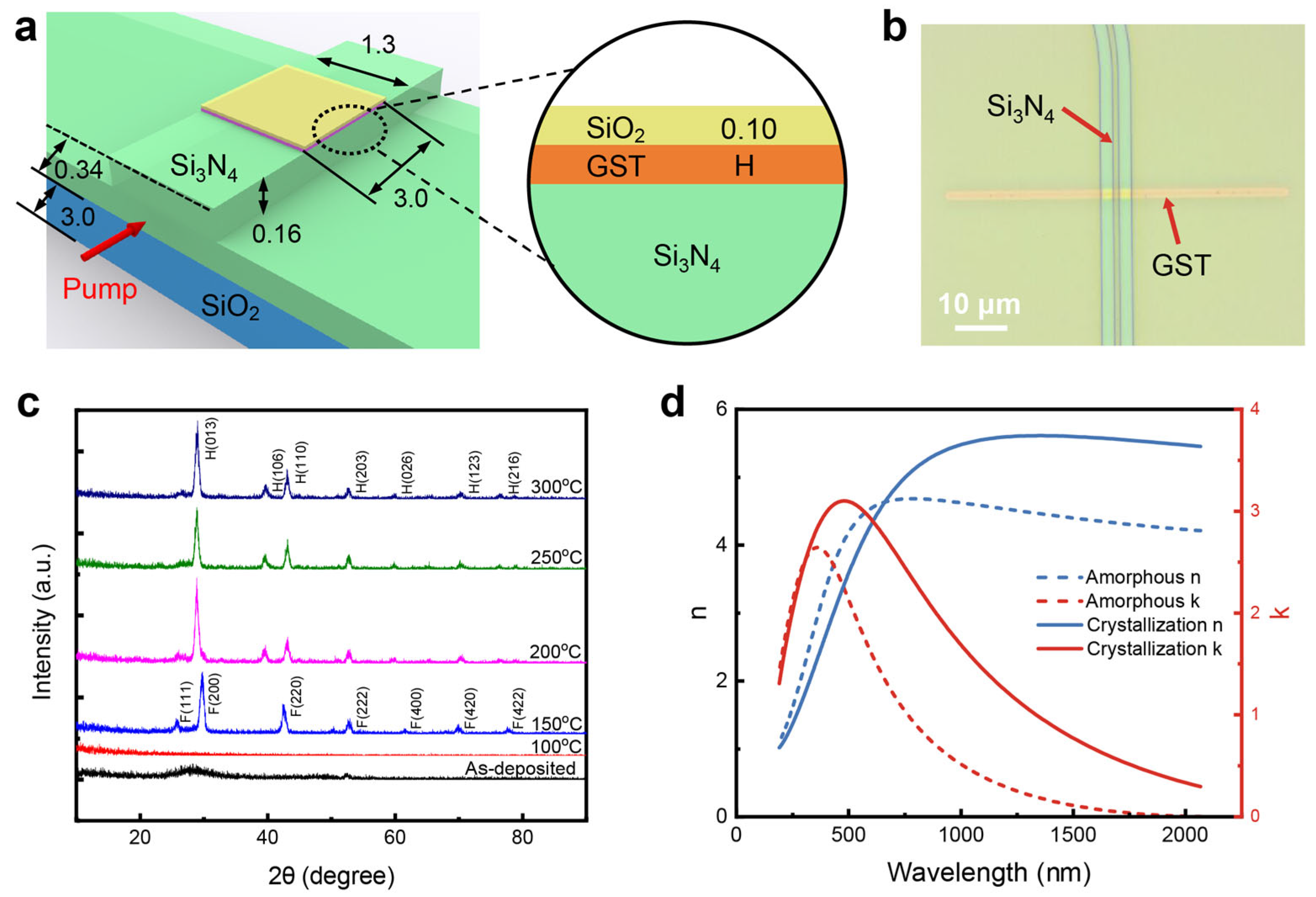
Figure 1. Integrated photonic phase-change memory. (a) Schematic diagram showing the device architecture with key dimensional parameters (units in μm). H, thickness of PCM. (b) Optical micrograph of the fabricated photonic memory cell. (c) X-ray diffraction patterns of GST films after thermal annealing at varying temperatures, demonstrating crystallization evolution. (d) Optical constant (n, k) spectra characterizing GST thin films across broad spectral bandwidths (190–2000 nm).
Photonics 12 01130 g001
Figure 2. Performance of photonic phase-change memory with optimized GST cell thickness. (a) Simulated transmission of amorphous (Ta) and crystalline (Tc) states, and their ratio (Ta/Tc) as functions of GST cell thickness (H). (b) Retention characteristics showing stable amorphous and crystalline states over time. (c) Transmission modulation versus programming pulse energy during the amorphization process. (d) Readout performance: output detection energy versus input probe energy in the lowest transmission state (crystalline). (e) Endurance test showing reversible switching between amorphous and crystalline states over 6000 cycles at the maximum transmission contrast. (f) Multi-level storage capability demonstrating 209 distinct transmission states (inset highlights states 75–125 for clarity).
Photonics 12 01130 g002
Figure 3. FDTD simulations of integrated photonic phase-change memory with engineered GST nanopatterns. (a) Schematic diagram of GST nanostructures on a Si3N4 waveguide platform. (bd) Simulated TE-mode electric field profiles (E) at the waveguide surface for three GST configurations, comparing amorphous (top) and crystalline (bottom) states: continuous 20 nm-thick GST film covering (2 μm along the waveguide) (b); hybrid structure of 10 nm planar GST with a nanodisc array (100 nm diameter, 50 nm height, 200 nm pitch) (c); fully etched embedded nanodisc array (identical dimensions to (c)) (d).
Photonics 12 01130 g003
Figure 4. Fabrication and performance of photonic phase-change memory with the GST nanopatterns. (a) Schematic of the GST micro-cylinder array integrated with a photonic waveguide. (b) SEM image of the fabricated GST nanopattern array. (c) Key fabrication steps: (i) waveguide patterning, (ii) GST deposition, (iii) nanodisc patterning, and (iv) protective encapsulation. Dark blue, Si3N4 layer; light blue, Al2O3 layer 1; yellow, GST layer; gray, Al2O3 layer 2. (d) Endurance test showing reversible phase switching over 2 × 10⁶ cycles at the maximum transmission contrast.
Photonics 12 01130 g004
Table 1. Tra, Trc and Tra/Trc of photonic phase-change memory with different nanopatterns.
Film Layer Height (nm)Micro-Cylinder Height (nm)TraTrcTra/Trc (dB)
2000.5500.04510.850
10500.4430.0459.925
5500.7950.1437.450
0500.8940.6731.233
Table 2. Performance comparison of reported photonic non-volatile phase-change devices.
Ref.MaterialsStructureModulation Speed (ns)Consumption
(pJ/Operation)
Storage Density
(Bit)
Endurance
(Cycles)
This workGSTHeight-optimized film
(nanodisc array)
100.967.716000 (film)
2 × 10⁶ (array)
[29]GSTUniform film256805.09--
[30]GSTUniform film +
PIN junction + DC 1
2003.8 × 105--2800
[31]N-GST 2Uniform film +
ITO heater 3
5 × 10⁴--7.79400
[16]SbUniform film8 × 10−4452.8150
[18]Sb2Se3Uniform film (sub-cell array) + PIN junction + MZI1006.4 × 1045 (film)
6 (array)
3000 (film)
1 × 10⁴ (array)
[32]Sb2S3Uniform film + PIN junction5001.22 × 10632500
[33]Sb2S3Uniform film + PIN junction1505.6 × 1045800
1 Directional coupler. 2 N-doped GST. 3 Indium tin oxide heater.
Disclaimer/Publisher’s Note: The statements, opinions and data contained in all publications are solely those of the individual author(s) and contributor(s) and not of MDPI and/or the editor(s). MDPI and/or the editor(s) disclaim responsibility for any injury to people or property resulting from any ideas, methods, instructions or products referred to in the content.