Article

Multi-Peak Narrowband Perfect Absorber Based on the Strong Coupling Between Fabry–Perot Mode and SPP Waveguide Mode

1
State Key Laboratory of Extreme Environment Optoelectronic Dynamic Testing Technology and Instrument, Nanjing University of Science and Technology, Nanjing 210094, China
2
School of Electronic and Optical Engineering, Nanjing University of Science and Technology, Nanjing 210094, China
*
Author to whom correspondence should be addressed.
Photonics 2025, 12(11), 1131; https://doi.org/10.3390/photonics12111131 (registering DOI)
Submission received: 28 September 2025 / Revised: 5 November 2025 / Accepted: 13 November 2025 / Published: 15 November 2025

Abstract

Plasmonic- or metamaterial-based multi-narrowband perfect absorbers hold significant potential applications in filtering, photodetection, and spectroscopic sensing. However, it is rather challenging to realize multi-peak and narrowband absorption simultaneously only using plasmonic metallic materials due to the single or dual resonance and large optical losses in the metallic nanostructure. Here, we numerically demonstrate a new multi-narrowband perfect absorber based on the strong coupling between the Fabry–Perot cavity modes and the surface plasmon polariton waveguide modes in a nanostructure consisting of periodic Ag grating and Ag film separated by a SiO2 waveguide layer. Six absorption peaks, an ultranarrow absorption resonance with FWHM as narrow as 8 nm, and an absorption peak amplitude surpassing 95% have been achieved. Furthermore, the optical properties of the designed nanostructures can be precisely tuned by modulating the grating period, slit width, height, as well as the thickness and refractive index of the waveguide layer. This approach establishes a versatile platform for designing high performance multi-narrowband absorbers, with promising applications in optical filters, nonlinear optics, and biosensors.

1. Introduction

Surface plasmon polaritons (SPPs) are electromagnetic waves that propagate along the interface between a metal and a dielectric medium, which result from the coupling between optical fields and collective electron oscillations at the metal/dielectric interface. Noble metals like Cu, Ag, and Au are particularly effective at supporting SPP excitation within the visible wavelength band, as their performance is highly dependent on microstructural properties such as composition, shape, and size. Consequently, the excitation wavelength of SPPs can be precisely tuned by altering the metal’s microstructure through different micro/nanofabrication technology [1,2], thereby providing an effective method for investigating plasmonic and metamaterial electromagnetic absorbers. Plasmonic or metamaterial perfect absorbers have attracted wide attention due to their significance in science and practical applications, such as thermal emitters [3], heat-assisted magnetic recording [4], solar steam generation [5], biosensors [6], and hot electron-based photodetection [7,8]. Over the past decade, numerous plasmonics or metamaterial perfect absorbers based on different metallic nanostructures have been extensively investigated theoretically and experimentally [9,10,11,12]. For example, the metal–insulator–metal (MIM) structure is advantageous for tightly confining the electromagnetic field on resonance [10]. Nonetheless, such plasmonic metamaterials typically exhibit broad absorption bandwidths due to strong radiative damping and intrinsic metal losses. This characteristic severely impedes their applications in color filters, thermal radiation tailoring, and sensors, where ultra-narrowband spectral response is essential [13,14].
To solve this problem, the mechanism of coupling plasmonic mode with plasmonic mode or photonic mode (Fabry–Perot mode, cavity mode, waveguide mode) was proposed to realize the narrowband perfect absorber. For example, Koray Aydin et al. demonstrated an ultra-narrowband absorber based on the surface lattice resonances of Au-nanoring and the nanowire arrays reflecting Au metallic film substrate [15]. Ye et al. realized the double narrowband resonances through the plasmonic mode coupling between the localized surface plasmon resonance (LSPR) mode of the Au-nanoring array and the cavity modes of the Au–SiO1–Au structure [16]. Chen et al. achieved an ultra-narrowband perfect absorber with significant electric field enhancement through the strong interaction between the magnetic plasmon in metallic split-ring resonators and the optical cavity modes of Fabry–Perot (FP) cavity [17]. Although there have been many research publications about utilizing the electromagnetic mode coupling mechanism to achieve narrowband perfect absorption mentioned above, there are few results related to the Fabry–Perot modes in the grating slit and the SPP waveguide mode in the dielectric layer. In addition, due to the dependence on the excitation of plasmonic or optical resonances, most of the proposed metamaterial absorbers only have one or two resonance wavelengths other than multi-wavelengths, which greatly limits its application in which multiband resonances are necessary [18,19,20,21], so it is important to study and design multi-narrowband metamaterial perfect absorbers.
In this paper, we proposed and numerically demonstrated a new multi-narrowband perfect absorber based on the strong coupling of the Fabry–Perot cavity resonance mode and the SPP waveguide mode in the Ag periodic grating/SiO2 spacer/Ag film structure. Through systematic simulations, we demonstrated the multi-narrowband absorber with six absorption peaks and an ultra-narrow absorption bandwidth of 8 nm with peak absorption exceeding 95%. A comprehensive investigation of the spectral characteristics reveals the coupling mechanism between FP mode and waveguide modes by varying key structural parameters, including Ag-grating height, period, and slit width. Furthermore, the effect of the thickness and refractive index of dielectric spacer on the optical properties were also investigated. Our findings offer a robust platform for designing high performance multi-narrowband absorbers, with promising applications in color filter, thermophotovoltaic narrowband emitter, and plasmonic biosensing technology.

2. Modeling and Simulation

Figure 1a shows the schematic of the proposed nanostructure, in which a dielectric spacer waveguide layer is inserted between the Ag gratings and the Ag film, where h indicates grating height, w is the slit width, H and nd are the thickness and refractive index of spacer (here is SiO2), respectively, P is the grating period, and t1 is the thickness of Ag film (unless otherwise specified, t1 is fixed at 200 nm). This nanostructure can be fabricated by using a combination of electron beam lithography and a subsequent lift-off process [22,23]. The real specific area of the nanostructure is determined by how large area is needed for application scenarios. We calculated the optical properties of the nanostructure with the finite-difference time-domain (FDTD) method [24,25]. To realize high precision, the nanostructure was assumed to be infinitely long in y direction, so we built a 2D model and used one period of the nanostructure in the following simulation; the periodic boundary condition was set in ±x direction and perfectly matched layers (PMLs) was set in ±z direction under normal TM-polarized incidence, and the spatial mesh grids are set as ∆x = ∆z = 2 nm, respectively. All absorption spectra were normalized to the incident light power. The optical permittivity data of silver were sourced from Palik [26]. The nanostructure was illuminated with normally incident light in an air environment. In the real experiment, the environment (such as temperature, air pressure, and humidity) change will affect the refractive index of air. Here we fixed the refractive index of air at 1.0.

3. Results

Figure 1b presents absorption spectra of the proposed nanostructure and the reference periodic Ag grating structure with P = 500 nm, w = 100 nm, H = 400 nm, and h = 400 nm. Owing to the opaque Ag film, the transmission channel is canceled and we can obtain the absorption A by A = 1 − R. Six obvious absorption peaks and a small absorption peak at λ0 = 519 nm are observed for the proposed nanostructure. The absorption A is high at 81%, 95.4%, 98.5%, 80.2%, 92.8%, 54.6% for λ1 (500 nm), λ2 (591 nm), λ3 (676 nm), λ4 (716 nm), λ5 (792 nm), λ6 (1147 nm), respectively. And the bandwidth values of these absorption peaks at λ1, λ2, λ3, λ4, λ5 and λ6 are 4 nm, 3 nm, 8 nm, 18 nm, 8 nm, and 60 nm, respectively. In contrast, the reference Ag grating without SiO2 spacer (H = 0 nm) shows only one dominant peak at 771 nm and a weaker peak at λ0 = 519 nm. This comparison clearly demonstrates that introducing SiO2 waveguide layer between the Ag grating and Ag film enables the multi-narrowband perfect absorption. In addition, due to the coupling of the Fabry–Perot resonance mode and waveguide mode, a Fano-like resonance with an asymmetric line shape can be clearly observed at λ3 = 676 nm and λ4 = 716 nm in Figure 1b. Multiband absorbers proposed by other researchers in recent years were compared to evaluate the performance of the proposed nanostructures [23,27,28,29]. The results are summarized in Table 1.
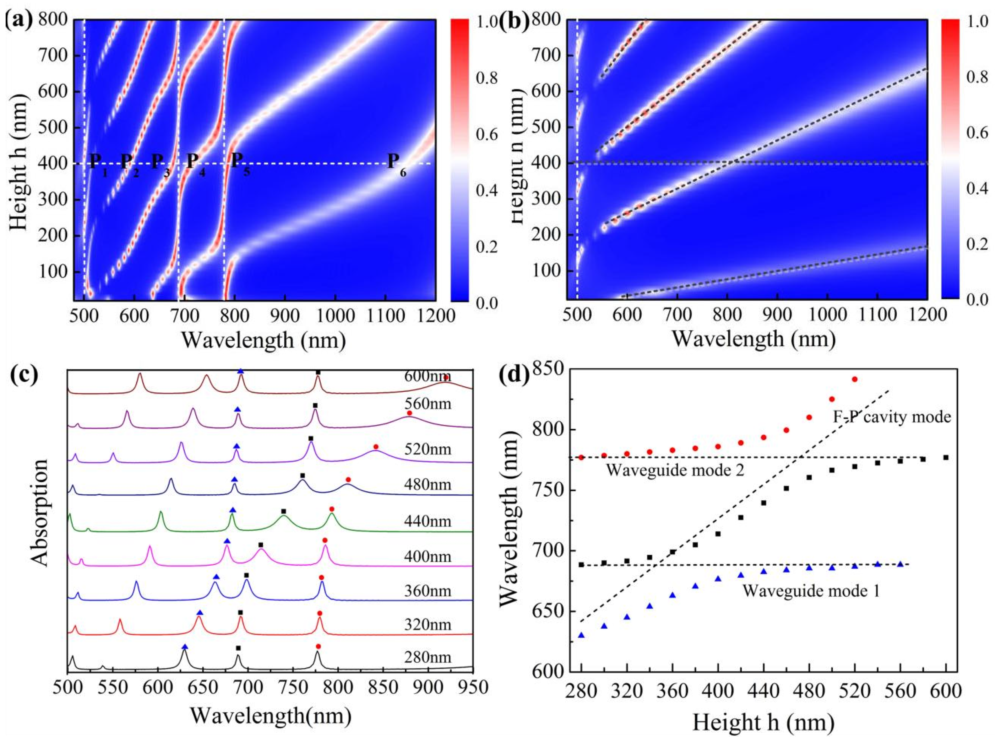
The influence of grating height h on the absorption spectrum of the proposed nanostructure and the reference grating is shown in Figure 2a,b, respectively. The slit supports the Fabry–Perot cavity resonance mode when the grating height h satisfies the resonance condition [30]. So, the absorption is greatly enhanced when Fabry–Perot resonance is excited as shown in Figure 2b. The black dashed lines correspond to Fabry–Perot resonance modes of different orders, which increase with the grating height. In contrast, the absorption spectrum of the proposed nanostructure (Figure 2a) not only exhibits the characteristic of Fabry–Perot modes, but also possesses two additional higher absorption bands (the vertical dashed lines). Moreover, compared to reference grating, the absorption peaks associated with Fabry–Perot resonance of Figure 2a show a difference depending on the metallic grating height h, and this behavior can be ascribed to the different phases obtained at the termination of the metallic slits (SiO2 dielectric layer) [31].
Furthermore, the six absorption peaks with h = 400 nm from left to right in Figure 1b are denoted by P1, P2, P3, P4, P5, and P6, respectively. The wavelength of P4 and P5 remains constant with the increased grating height h, suggesting that these peaks are independent of the electromagnetic field distribution within the metal slits. In other words, the appearance of peak P4 and P5 has no relation with the cavity mode inside the metallic slits and the specific mechanism will be discussed later through the field distribution. Although peak P1 (500 nm) also remains constant with the increased grating thickness, the mechanism is not same as that of P4 and P5. Herein, the absorption peak (P1) is caused by the Wood Rayleigh anomaly, which is mainly determined by the period of the grating [32].
Figure 2a reveals an additional interesting aspect of the Fabry–Perot mode and the waveguide mode. As grating thickness h increases, the absorption peak (caused by Fabry–Perot mode) red-shifts, while the absorption peaks caused by the waveguide mode almost remain constant. The anti-crossing phenomenon takes place when the Fabry–Perot modes red-shift and interact with the SPP waveguide modes. To observe the anti-crossing behavior between the Fabry–Perot mode and waveguide mode more intuitively, Figure 2c,d displays the absorption spectra as the grating thickness increases from 280 nm to 600 nm. Apparently, as the height of the Ag grating increases, the absorption peak caused by the SPP waveguide mode (waveguide mode 1 and 2) kept nearly constant (the horizontal black dash line), while the wavelength of Fabry–Perot cavity mode (inclined black dash line) red-shifted and interacted with the waveguide mode. When the grating thickness reaches 480 nm, the Fabry–Perot cavity mode and SPP waveguide mode exhibits a repulsion behavior. For the spectrum of h = 520 nm, the Fabry–Perot cavity resonance occurs at λ = 830 nm, which is longer than that of SPP mode (λ = 792 nm). This simulation result clearly indicates the anti-crossing behavior in the proposed nanostructure, demonstrating the strong mode coupling between the Fabry–Perot cavity mode and the SPP waveguide mode.
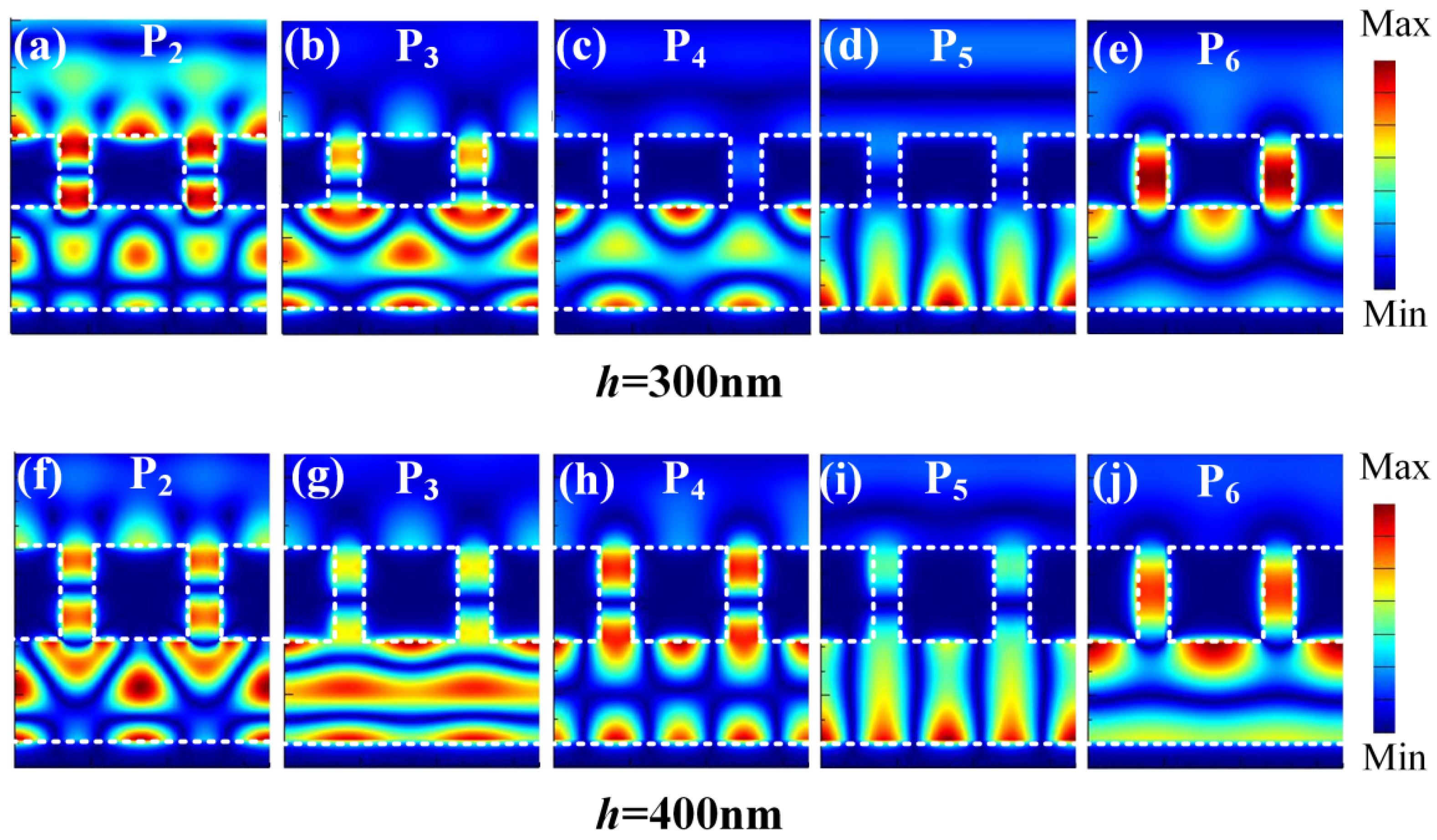
To further understand the physical origin of the multiple narrowband absorption peaks and the Fano-like resonance with an asymmetric line-shape of the proposed nanostructure, we calculated the magnetic field distribution pattern of the different absorption peak wavelength (P1, P2, P3, P4, P5, and P6) with grating thicknesses of 300 nm and 400 nm (the structure parameter are P = 500 nm, w = 100 nm, and H = 400 nm), respectively. As mentioned above, the peak P1 is caused by the Wood Rayleigh anomaly, so the field distribution of peak P1 is not shown here. As shown in the first row of Figure 3 (h = 300 nm), the second order, first order and first order vertical FP cavity mode are excited in the grating slit at peak P2, P3, and P6, respectively. For peaks P4 and P5, the magnetic field is mainly concentrated at the Ag-grating/SiO2 interface or the interface between the SiO2/Ag film, showing the characteristic of SPPs along the x direction, which is also regarded as the waveguide mode in the dielectric waveguide on Ag film. Under the condition of h = 400 nm, the peak wavelength and field distribution pattern of P5 almost remain unchanged. Peaks P2 and P6 redshift with the increased grating thickness and do not couple with the other mode, so the field pattern is also same as that of h = 300 nm. But for the peak P3, the cavity resonance red-shifts and interacts with the waveguide mode at P4, so the field pattern experiences a big change, as shown in Figure 3g,h. Therefore, it is convenient to adjust the mode coupling between the Fabry–Perot mode and the SPP waveguide mode and realize the multi-narrowband absorption by tuning the grating height h.
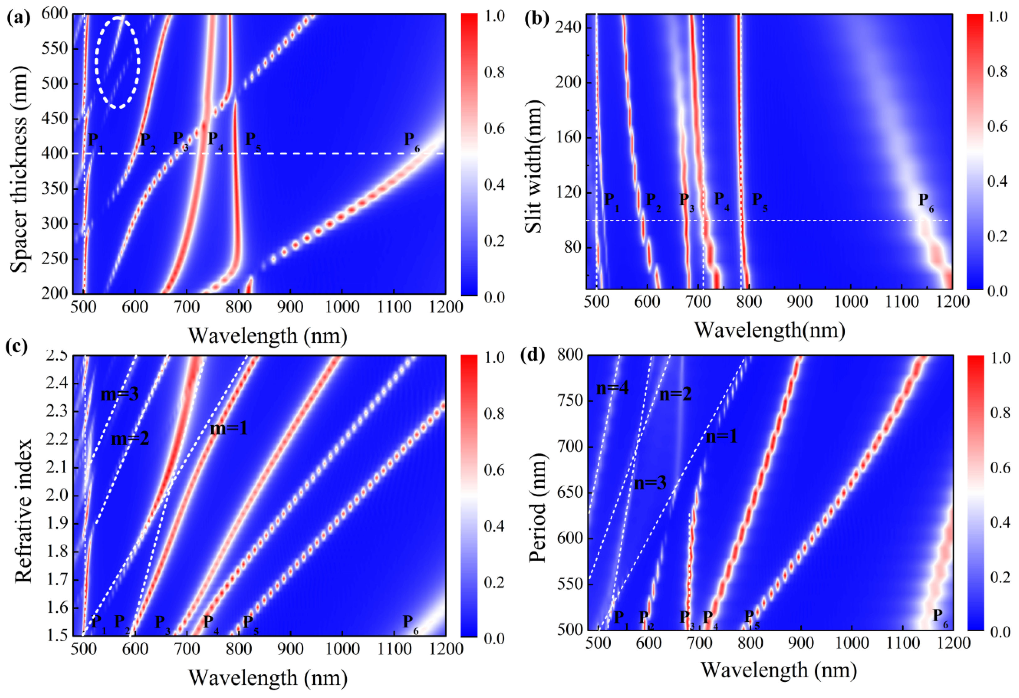
In order to further understand the characteristics of these narrowband absorption peaks and the anti-crossing behavior, we have also systematically investigated the effects of geometric parameters on the optical properties of the proposed nanostructures in Figure 4 by individually changing H, w, nd, or P from the base values given in Figure 1 (P = 500 nm, w = 100 nm, H = 400 nm, h = 400 nm, nd = 1.5). The effect of SiO2 waveguide thickness on the absorption is shown in Figure 4a, and the value of absorption peak increases with the increased SiO2 film thickness H, which can be attributed to the illustration that the thicker dielectric layer can support more waveguide modes [33]. The SiO2 thickness H increases from 200 nm to 600 nm, and the absorption peak increases from five to eight (short dash circle in Figure 4a).
The effect of slit width w on the absorption spectra of the nanostructures with parameters fixed at h = 400 nm, P = 500 nm, H = 400 nm, and nd = 1.5 under TM-polarized light normal incident is shown in Figure 4b. The peak wavelength of P1, P4, and P5 remains almost constant with the increased slit width. As described above, the absorption peak P1 is caused by the Wood Rayleigh anomaly, so it is independent of the slit width. Peak P4 and P5 are caused by the SPP waveguide mode, and therefore their resonance wavelengths are also independent of the slit width. However, the P2, P3, and P6 are mainly induced by the cavity resonance in the Ag-grating slit, which causes the peak wavelength to be strongly dependent on the slit width and blue-shift with the increased slit width, which matches well with the previous theory [32]. In addition, with the increased slit width, peak P4 generates an anti-crossing with peak P3, so the Fano-type resonance wavelength can also tailored by adjusting the slit width.
Figure 4c presents the effect of the refractive index nd of the waveguide layer on the absorption spectra of the proposed nanostructures with w = 100 nm, t = 400 nm, P = 500 nm, and H = 400 nm. Except P1, the absorption peaks (P2, P3, P4, P5, P6) all have an obvious red-shift with the increased refractive index nd. For P2, P3, and P6, the red-shifts are caused by the different phase changes at the termination of the slit. For P4 and P5, the SPP waveguide mode is sensitive to the dielectric environment [34]. In addition, when the index grows up to 1.6, new absorption peaks (labeled as m = 1, m = 2, m = 3) arise in the short wavelength region. The mechanism is similar to that of the new absorption peaks induced by the increased thickness of waveguide layer in Figure 3a. According to SPP waveguide theory [34], the number of transmission modes in the waveguide is strongly dependent on the thickness and refractive index of the waveguide. In addition, when the P2 mode red-shifts with the increased refractive index, it anti-crosses with the higher order waveguide mode (which is labeled as m = 1).
Figure 4d shows the influence of grating period P on the absorption spectra of the proposed nanostructure when it increases from 500 nm to 800 nm. The resonant wavelength of the Fabry–Perot mode at 591 nm (P2) and 676 nm (P3) only slightly shift (even unchanged for P3) with the change in period P, except for the region (larger than 650 nm) of coupling with the Wood–Rayleigh anomaly mode (white dash line label as n = 1). When the Fabry–Perot cavity modes couple with the Wood–Rayleigh anomaly mode, the resonance bandwidth drastically decreases. The resonance peaks at λ4 = 716 nm (P4) and λ5 = 792 nm (P5) are caused by the first order SPP mode at the Ag-grating/SiO2 interface and SiO2/Ag film interface, respectively. So, these modes possess the characteristic of the SPP mode, and the absorption peaks red-shift with the increased period P.
In addition, with the increased period P, higher-order SPP waveguide modes occur, and the dash lines labeled by n = 2 and n = 4 respond to the second order SPP mode and third-order SPP mode at the SiO2/Ag film interface, respectively. The white dash line labeled as n = 3 responds to the second order SPP mode propagating along the Ag-grating/SiO2 interface. As mentioned above, the peak P6 is caused by the Fabry–Perot cavity mode in the grating slit, so it is original and did not vary with the period P, but with the increased period, the wavelength of P5 red-shifts and couples with P6, so peak P6 will red-shift with the increased period P. Therefore, the resonance absorption behavior of the proposed nanostructure can be adjusted by selecting suitable structural parameters. In addition, it has to be noted that the period P, grating height H, and dielectric thickness h have a big influence on the optical properties, and the slit width w has a small effect on the optical properties; therefore, in the fabrication process, the period P, grating height H, and dielectric thickness h should be precisely controlled.
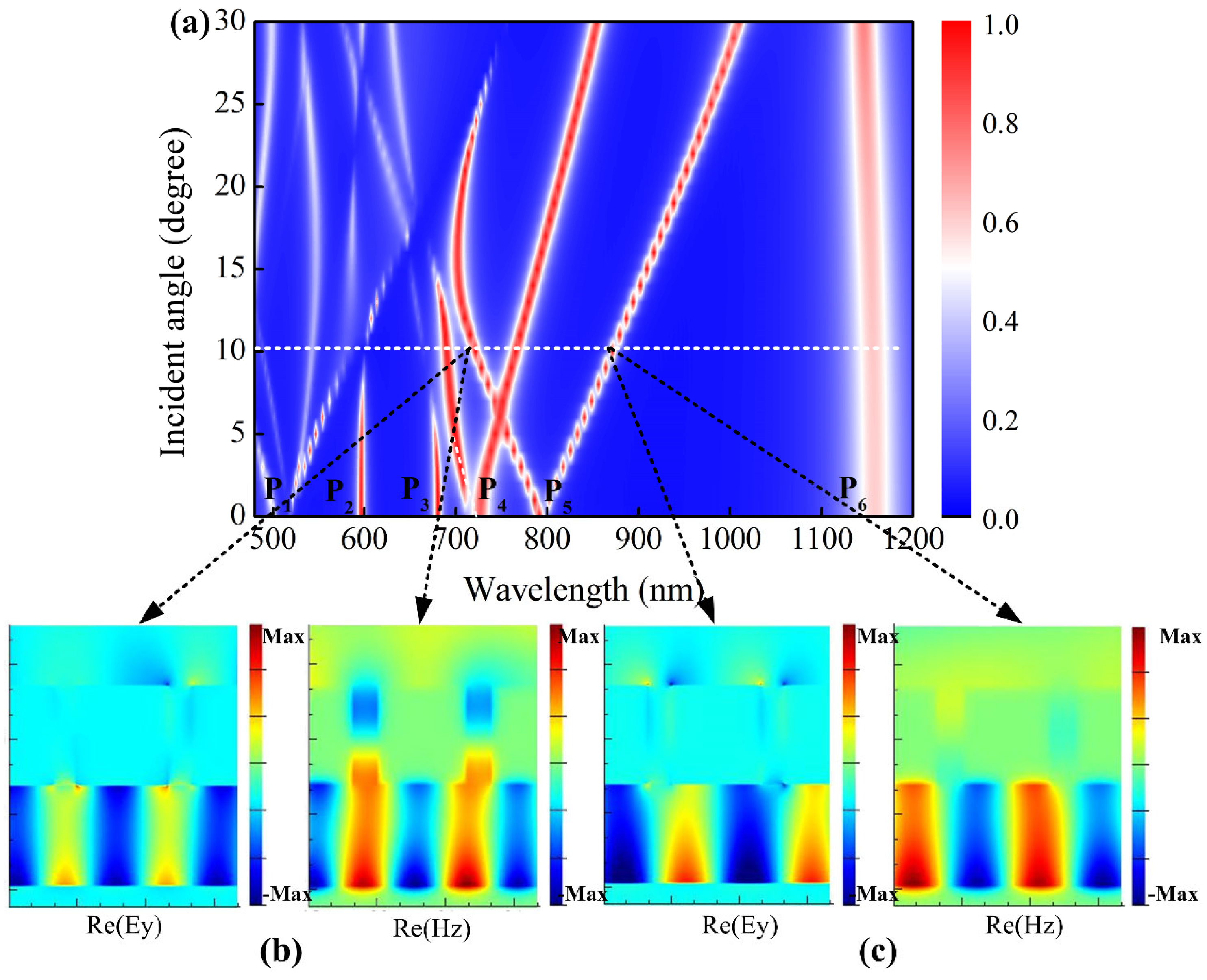
The influence of oblique incident light on the absorption spectra of the nanostructure (P = 500 nm, w = 100 nm, H = 400 nm, h = 400 nm) was also investigated as shown in Figure 5. The peaks P4 and P5 at normal incidence split into two absorption peak bands (but still kept the narrowband) when the incident angle increased from 0 to 30 degree. As mentioned above, the peaks P4 and P5 are caused by the excitation of SPP (P4, P5). At oblique incidence, the two split absorption peak bands correspond to the excitation of two SPPs with opposite wave vectors in x direction of propagation on the Ag/SiO2 interface. In contrast, the Fabry–Pérot (FP) cavity resonance is inherently angle-independent. Consequently, the wavelength positions of peaks P2, P3, and P6 relate to the FP cavity mode within the grating slit, which remains nearly constant for incident angles up to 8°. However, at larger angles (>8°), the split SPP modes interact with the FP cavity mode, inducing strong coupling between the two [35]. This hybridization results in a mixed mode, exhibiting characteristics of both resonances, thereby causing the FP cavity mode to shift with the incident angle.
To deeply elucidate the physical mechanism of the excitation of the two SPPs at the Ag/SiO2 interface, Figure 5b,c shows the distribution of the real part of the electric field (Ey) and the magnetic field (Hz) at incident angles of 10° for wavelengths of 723 nm and 875 nm, respectively. Evidently, electromagnetic fields are strongly localized at the SiO2 waveguide dielectric/Ag film interface. An exponential decay of the electric field (Ey) along the z-direction is observed. While the spatial distribution of Ey is similar for both wavelengths (723 nm and 875 nm), the spatial distribution of Hz exhibits opposite profiles. According to the fundamental properties of electromagnetic plane waves, the components kx, Ey, and Hz satisfy the right-hand rule, where kx represents the wave vector of the SPPs at the SiO2 waveguide/Ag interface along the x-direction. Therefore, we conclude that the SPPs at the SiO2 waveguide/Ag interface for 723 nm and 875 nm propagate in opposite directions along x. This confirms that the two excited SPP modes possess opposite wave vectors in the x-direction. In summary, the splitting of absorption resonances (modes P4 and P5) with the incident angle, as observed in the SPP modes, demonstrates that our theoretical explanations are in excellent quantitative agreement with the FDTD simulation results. It should be noted that the proposed nanostructure consists of one-dimensional grating, so the optical properties would be sensitive to the polarization state of incident light. In the future, we can realize the polarization-insensitive multi-narrowband perfect absorber by designing the 2D grating or nanopillar array (distributed in quadrangle or orthohexagnal) [29,36] on the top of the nanostructure.

4. Conclusions

In summary, a new multi-narrowband perfect absorber consisting of periodic Ag-grating and Ag film separated by a SiO2 waveguide layer has been proposed and investigated. Six ultrasharp absorption resonance with a minimum bandwidth as narrow as 8 nm and an absorption peak amplitude surpassing 95% were obtained at normal light incidence. Numerical simulations demonstrate that the multi-narrowband absorption arises from the Fabry–Perot resonance in the slit coupling with the propagating SPP waveguide mode at the SiO2/Ag-grating or Ag film interface. Moreover, the simulation results imply that the absorption properties are sensitive to structural parameters and the refractive index of waveguide layer, indicating the spectra tunability and selectivity of the proposed nanostructure. Those findings may offer valuable insights for the designing of multi-narrowband perfect absorbers, which could easily find significant applications in filters, nonlinear optics, and biosensors, where multi-ultranarrow band perfect absorption is necessary.

Author Contributions

Conceptualization, Y.Z.; methodology, Y.Z.; software, Y.Z.; validation, Y.Z.; formal analysis, Y.Z.; investigation, Y.Z.; resources, W.H.; data curation, Y.Z.; writing—original draft preparation, W.H.; writing—review and editing, Y.Z. and W.H.; visualization, Y.Z.; supervision, W.H.; project administration, Q.C.; funding acquisition, Y.Z. All authors have read and agreed to the published version of the manuscript.

Funding

This research was funded by the National Natural Science Foundation of China (61805037), Fundamental Research Funds for the Central University (No. 30925010513).

Institutional Review Board Statement

Not applicable.

Informed Consent Statement

Not applicable.

Data Availability Statement

Data are contained within the article.

Conflicts of Interest

The authors declare that there are no conflicts of interest related to this article.

References

  1. Lameirinhas, R.A.M.; Torres, J.P.N.; Baptista, A.; Martins, M.J.M. A New Method to Analyse the Role of Surface Plasmon Polaritons on Dielectric-Metal Interfaces. IEEE Photonics J. 2022, 14, 2236409. [Google Scholar] [CrossRef]
  2. Maleki, M.J.; Soroosh, M.; Akbarizadeh, G. A compact low-loss 2-to-4 plasmonic decoder based on suspended graphene for surface plasmon polariton transmission. Diam. Relat. Mater. 2024, 144, 110983. [Google Scholar] [CrossRef]
  3. Liu, X.; Tyler, T.; Starr, T.; Starr, A.F.; Jokerst, N.M.; Padilla, W.J. Taming the blackbody with infrared metamaterials as selective thermal emitters. Phys. Rev. Lett. 2011, 107, 045901. [Google Scholar] [CrossRef]
  4. Stipe, B.C.; Strand, T.C.; Poon, C.C.; Balamane, H.; Boone, T.D.; Katine, J.A.; Li, J.-L.; Rawat, V.; Nemoto, H.; Hirotsune, A. Magnetic recording at 1.5 Pb m−2 using an integrated plasmonic antenna. Nat. Photonics 2010, 4, 484–488. [Google Scholar] [CrossRef]
  5. Zhou, L.; Tan, Y.; Ji, D.; Zhu, B.; Zhang, P.; Xu, J.; Gan, Q.; Yu, Z.; Zhu, J. Self-assembly of highly efficient, broadband plasmonic absorbers for solar steam generation. Sci. Adv. 2016, 2, e1501227. [Google Scholar] [CrossRef] [PubMed]
  6. Liu, N.; Mesch, M.; Weiss, T.; Hentschel, M.; Giessen, H. Infrared perfect absorber and its application as plasmonic sensor. Nano Lett. 2010, 10, 2342–2348. [Google Scholar] [CrossRef] [PubMed]
  7. Li, W.; Valentine, J. Metamaterial perfect absorber based hot electron photodetection. Nano Lett. 2014, 14, 3510–3514. [Google Scholar] [CrossRef] [PubMed]
  8. Nan, X.; Lai, W.; Peng, J.; Wang, H.; Chen, B.; He, H.; Mo, Z.; Xia, Z.; Tan, N.; Liu, Z.; et al. In situ photoelectric biosensing based on ultranarrowband near-infrared plasmonic hot electron photodetection. Adv. Photonics 2024, 6, 026007. [Google Scholar] [CrossRef]
  9. Landy, N.I.; Sajuyigbe, S.; Mock, J.; Smith, D.; Padilla, W. Perfect metamaterial absorber. Phys. Rev. Lett. 2008, 100, 207402. [Google Scholar] [CrossRef]
  10. Hao, J.; Wang, J.; Liu, X.; Padilla, W.J.; Zhou, L.; Qiu, M. High performance optical absorber based on a plasmonic metamaterial. Appl. Phys. Lett. 2010, 96, 251104. [Google Scholar] [CrossRef]
  11. Liu, G.; Liu, Y.; Tang, L.; Liu, X.; Fu, G.; Liu, Z. Semiconductor-enhanced Raman scattering sensors via quasi-three-dimensional Au/Si/Au structures. Nanophotonics 2019, 8, 1095–1107. [Google Scholar] [CrossRef]
  12. Chen, Y.; You, K.; Lin, J.; Zhao, J.; Ma, W.; Meng, D.; Cheng, Y.; Liu, J. Design of a Broadband Perfect Solar Absorber Based on a Four-Layer Structure with a Cross-Shaped Resonator and Triangular Array. Photonics 2022, 9, 565. [Google Scholar] [CrossRef]
  13. Liu, Z.; Liu, G.; Liu, X.; Huang, S.; Wang, Y.; Pan, P.; Liu, M. Achieving an ultra-narrow multiband light absorption meta-surface via coupling with an optical cavity. Nanotechnology 2015, 26, 235702. [Google Scholar] [CrossRef]
  14. Zhang, M.; Fang, J.; Zhang, F.; Chen, J.; Yu, H. Ultra-narrow band perfect absorbers based on Fano resonance in MIM metamaterials. Opt. Commun. 2017, 405, 216–221. [Google Scholar] [CrossRef]
  15. Li, Z.; Butun, S.; Aydin, K. Ultranarrow band absorbers based on surface lattice resonances in nanostructured metal surfaces. ACS Nano 2014, 8, 8242–8248. [Google Scholar] [CrossRef]
  16. Liu, Z.; Ye, J. Highly controllable double Fano resonances in plasmonic metasurfaces. Nanoscale 2016, 8, 17665–17674. [Google Scholar] [CrossRef] [PubMed]
  17. Chen, S.; Li, G.; Lei, D.; Cheah, K.W. Efficient energy exchange between plasmon and cavity modes via Rabi-analogue splitting in a hybrid plasmonic nanocavity. Nanoscale 2013, 5, 9129–9133. [Google Scholar] [CrossRef]
  18. He, X.; Jie, J.; Yang, J.; Han, Y.; Zhang, S. Asymmetric dielectric grating on metallic film enabled dual- and narrow-band absorbers. Opt. Express 2020, 28, 4594. [Google Scholar] [CrossRef]
  19. Qin, L.; Liu, F.; Yuan, F.; Zhang, A.; Zhang, K. An angle-tuned polarization-independent multi-narrowband perfect absorber. J. Opt. 2022, 24, 095002. [Google Scholar] [CrossRef]
  20. Yang, C.; Shen, W.; Zhang, Y.; Zhao, D.; Liu, X. Multi-narrowband absorber based on subwavelength grating structure. Opt. Commun. 2014, 331, 310–315. [Google Scholar] [CrossRef]
  21. Wen, X.; Deng, S. Plasmonic Nanostructure Lattices for High-Performance Sensing. Adv. Opt. Mater. 2023, 11, 2300401. [Google Scholar] [CrossRef]
  22. Borui, L.; Yao, Z.; Tsai, D.P.; Shumin, X. Meta-device: Advanced manufacturing. Light Adv. Manuf. 2024, 5, 117–132. [Google Scholar]
  23. Liu, Y.; Ma, W.-Z.; Wu, Y.-C.; Meng, D.; Cheng, Y.-Y.; Chen, Y.-S.; Liu, J.; Gu, Y. Multi-peak narrow-band metamaterial absorber for visible to near-infrared wavelengths. Results Phys. 2023, 47, 106374. [Google Scholar] [CrossRef]
  24. Zhai, Y.; Chen, G.; Xu, J.; Qi, Z.; Li, X.; Wang, Q. Multiple-band perfect absorbers based on the combination of Fabry-Perot resonance and the gap plasmon resonance. Opt. Commun. 2017, 399, 28–33. [Google Scholar] [CrossRef]
  25. Taflove, A.; Hagness, S.C. Computational Electrodynamics: The Finite-Difference Time-Domain Method, 3rd ed.; Artech House: Norwood, MA, USA, 2005. [Google Scholar]
  26. Palik, E.D. Handbook of Optical Constants of Solids; Academic Press: Cambridge, MA, USA, 1998; Volume 3. [Google Scholar]
  27. Ai, Z.; Liu, H.; Cheng, S.; Zhang, H.; Yi, Z.; Zeng, Q.; Wu, P.; Zhang, J.; Tang, C.; Hao, Z. Four peak and high angle tilted insensitive surface plasmon resonance graphene absorber based on circular etching square window. J. Phys. D Appl. Phys. 2025, 58, 185305. [Google Scholar] [CrossRef]
  28. Cheng, R.; Zhou, Y.; Liu, J.; Hu, S.; Liu, H.; Pan, J.; Huang, W.; He, X.; Liang, B.; Zhang, L. Independently tunable multi-band terahertz absorber based on graphene sheet and nanoribbons. Opt. Express 2022, 30, 3893–3902. [Google Scholar] [CrossRef]
  29. Zhong, Q.; Wang, T.; Jiang, X.; Cheng, L.; Yan, R.; Huang, X. Near-infrared multi-narrowband absorber based on plasmonic nanopillar metamaterial. Opt. Commun. 2020, 458, 124637. [Google Scholar] [CrossRef]
  30. Zhou, W.; Wu, Y.; Yu, M.; Hao, P.; Liu, G.; Li, K. Extraordinary optical absorption based on guided-mode resonance. Opt. Lett. 2013, 38, 5393–5396. [Google Scholar] [CrossRef] [PubMed]
  31. Chen, X.; Yan, X.; Li, P.; Mou, Y.; Wang, W.; Guan, Z.; Xu, H. Mechanism of resonant perfect optical absorption in dielectric film supporting metallic grating structures. Opt. Express 2016, 24, 19435–19447. [Google Scholar] [CrossRef]
  32. Liang, Y.; Peng, W. Theoretical study of transmission characteristics of sub-wavelength nano-structured metallic grating. Appl. Spectrosc. 2013, 67, 49–53. [Google Scholar] [CrossRef]
  33. Liang, Y.; Peng, W.; Hu, R.; Xie, L. Extraordinary optical properties in the subwavelength metallodielectric free-standing grating. Opt. Express 2014, 22, 19484–19494. [Google Scholar] [CrossRef]
  34. Kaplan, A.F.; Xu, T.; Guo, L.J. High efficiency resonance-based spectrum filters with tunable transmission bandwidth fabricated using nanoimprint lithography. Appl. Phys. Lett. 2011, 99, 143111. [Google Scholar] [CrossRef]
  35. Ho, Y.L.; Huang, L.C.; Delaunay, J.J. Spectrally Selective Photocapacitance Modulation in Plasmonic Nanochannels for Infrared Imaging. Nano Lett. 2016, 16, 3094–3100. [Google Scholar] [CrossRef] [PubMed]
  36. Chen, Z.; Liu, M.; Cheng, S.; Wang, J.; Yi, Y.; Li, B.; Tang, C.; Gao, F. Bilayer graphene metasurface with dynamically reconfigurable terahertz perfect absorption. Curr. Appl. Phys. 2025, 80, 282–290. [Google Scholar] [CrossRef]
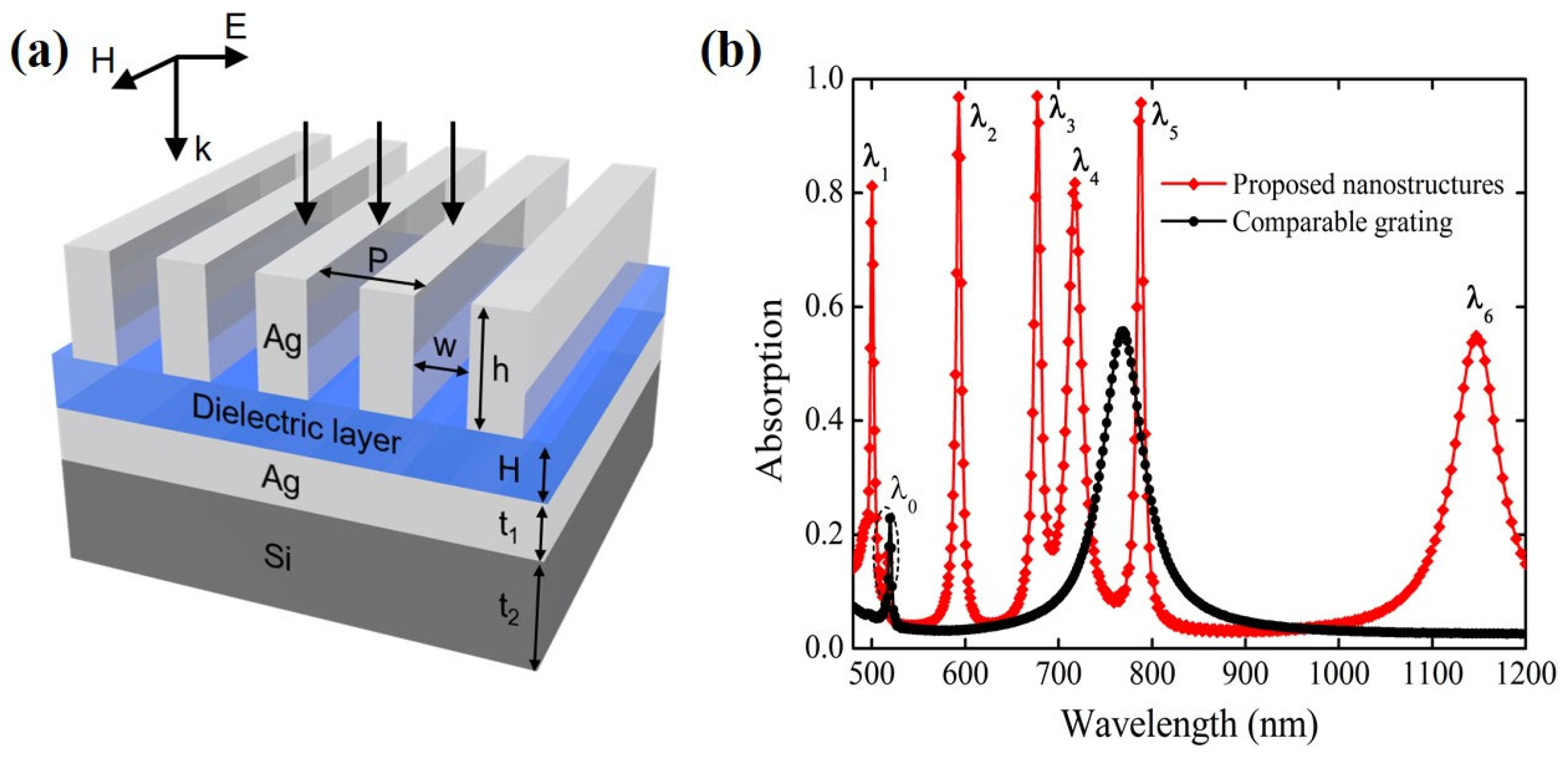
Figure 1. The schematic of the proposed Ag grating, SiO2 spacer, and an opaque Ag film on silicon substrate and its absorption spectra. (a) Schematic diagram and its structure parameters. (b) Calculated absorption spectrum under TM-polarized light and normal incidence with the thickness of SiO2 spacer layer (nd = 1.5) H = 400 nm (red line) and H = 0 nm (black line) (P = 500 nm; w = 100 nm; h = 400 nm).
Photonics 12 01131 g001
Figure 2. Absorption as function of wavelength and grating thickness h at normal incidence of the proposed structures (a) with fixed P = 500 nm, w = 100 nm, H = 400 nm, and (b) P = 500 nm, w = 100 nm, and H = 0 nm (i.e., without dielectric waveguide layer). The vertical white lines in Figure 2a indicate the waveguide modes, the horizontal dash line in Figure 2a indicate the position of h = 400 nm. (c) The absorption spectra with grating thickness h ranges from 360 nm to 600 nm (from down to top), in steps of 40 nm. (d) Resonance wavelength of the waveguide modes and the Fabry–Perot cavity mode as a function of the grating height h.
Photonics 12 01131 g002
Figure 3. The spatial magnetic field distribution pattern of the different absorption peaks wavelengths (P2, P3, P4, P5, P6) with grating thickness of 300 nm (ae) and 400 nm (fj), respectively.
Photonics 12 01131 g003
Figure 4. Contour plots show the absorption spectra of the proposed nanostructure at normal incidence depending on wavelength that varies with geometric parameter or refractive index: (a) spacer thickness H, the dash circle represent the higher order absorption peaks, (b) slit width w, (c) refractive index nd, and (d) grating period P.
Photonics 12 01131 g004
Figure 5. Dependence of absorption on both wavelength and incident angle for the proposed nanostructures. (a) Absorption spectra of nanostructure with the parameters fixed at P = 500 nm, w = 100 nm, h = 400 nm, and H = 400 nm. The vertical lines represent the Fabry–Perot modes in the slit of the metallic grating and the oblique dashed line corresponding to the SPP modes and the waveguide modes in the dielectric layer. (b) Real part distribution of electric field (Ey) and magnetic field (Hz) at an incident angle of 10 degree and a wavelength of 715 nm. (c) Real part distribution of electric field (Ey) and magnetic field (Hz) at an incident angle of 10 degree and a wavelength of 875 nm.
Photonics 12 01131 g005
Table 1. Result of proposed perfect absorber compared with other multiband absorbers.
ReferenceNumber of PeaksMaximum Peak
Absorption
FWHM (Full-Width at Half-Maximum)Wavelength
[27]498.5%~5 nm2200–2400 nm
[28]585.7%/5–100 um
[29]599.3%15 nm800–2000 nm
[23]599.9%5 nm750–3000 nm
Proposed698.5%8 nm450–1200 nm
Disclaimer/Publisher’s Note: The statements, opinions and data contained in all publications are solely those of the individual author(s) and contributor(s) and not of MDPI and/or the editor(s). MDPI and/or the editor(s) disclaim responsibility for any injury to people or property resulting from any ideas, methods, instructions or products referred to in the content.