1. Introduction
Terahertz (THz) technology is attracting increasing attention due to its applications in medical imaging, security screening, communication and materials characterization [
1,
2,
3,
4,
5,
6]. THz emitters are the key components to the application of THz systems, and the photoconductive antenna (PCA) technique is one of the most widely used techniques for THz emission due to its ease of use, compact size and potential for direct connection to fiber optics. When a femtosecond laser irradiates on the photoconductor, free carriers are generated and accelerated by the DC bias voltage. Then a transient photocurrent is formed and completely decays in a very short time. This ultra-short transient photocurrent generates THz radiation pulses. Beyond conventional PCA approaches, functional THz devices utilizing metasurfaces and novel materials such as graphene [
7] and Dirac semimetals [
8] have also undergone rapid advances in recent years, thereby significantly expanding the capabilities of THz systems. Compared with other THz generation technologies, photoconductive emitters can generate THz waves over a wide bandwidth range and have relatively low equipment costs and possess the advantages of high gain, small size and easy tuning [
9].
Despite their significant advantages, photoconductive THz emitters remain limited by low THz radiation power and insufficient bandwidth. Recent studies demonstrate that integrating plasmonic nanostructures into photoconductive emitters enhances light absorption in semiconductors and shortens the mean transport distance of photogenerated carriers to the contact electrodes. This approach significantly enhances THz radiation power and bandwidth, providing a novel strategy to overcome performance limitations in THz sources [
10,
11,
12,
13,
14,
15]. C. W. Berry et al. [
16] proposed embedding a plasmonic grating within a dipole THz PCA. By integrating grounded nanorods as electrode components, this design confined charge carrier transport paths to nanoscale distances from the electrodes, improving the collection efficiency of charge carriers and increasing the overall response of the PCA by an order of magnitude. S. H. Yang et al. [
17] suppressed the carrier transit time to sub-picosecond levels by using a three-dimensional plasmonic contact electrode. Under 1.4 mW pulsed-laser pumping conditions, the THz radiation power reached 105 μW across the 0.1~2 THz band, achieving a record 7.5% optical-to-terahertz conversion efficiency with a threefold increase in THz photocurrent.
When the laser power or bias electric field reaches a certain level, the radiated power of PCAs gradually tends to a saturation state. This significantly hinders the application and advancement of photoconductive emitters in THz technology. The shorter photocarrier transit times observed in small-aperture PCAs can be attributed to the smaller electrode gaps. Under these conditions, the principal source of the observed saturation effect is the space-charge shielding phenomenon, where the applied bias field is suppressed by the Coulomb electric field generated during the electron-hole separation process. It has been confirmed that the saturation effect observed in photoconductive emitters employing narrowed electrode gaps to shorten carrier transit time primarily arises from the space-charge shielding effect [
18,
19]. This effect hinders the acceleration process of photogenerated carriers, thereby limiting further improvement in radiated power.
Consequently, to mitigate the space-charge shielding effect in THz transmitters, several optimization strategies have been explored [
20,
21,
22,
23,
24,
25,
26]. Regarding gap structure design, A. Bhattacharya et al. [
20] proposed an embedded plasmonic metasurface structure in the substrate to introduce faster charge dynamics and increase the emission bandwidth of the PCAs by over 50%. This approach also improved the peak THz amplitude by nearly 100% at high pump power, attenuating the shielding effect of the electric field at high power. For electrode optimization, M. Khorshidi et al. [
21] designed a structure featuring three-stepped periodic metallic rods and embedded this structure into the electrodes of the PCA. This structure effectively regulates the spatial distribution of charge carriers. Compared to the rectangular metal rods, the three-stepped periodic metallic rods significantly expand the carrier generation region, suppress carrier recombination and alleviate the phenomenon of charge density aggregation at the electrode interface. Consequently, the influence of the shielding electric field is reduced. However, the embedded structure in the above designs exists considerable challenges for practical fabrication and mass production. At the level of external field control, D. Zhou et al. [
22] introduced additional electrode structures into photoconductive detectors to generate an external electric field. This approach optimizes the balance of the internal electric field distribution, enabling uniform spatial control of charge carrier distribution. Consequently, the space-charge shielding effect is suppressed, and device performance is enhanced. However, the introduction of these additional electrodes inevitably impacts the charge carrier collection process, resulting in a slower current pulse response and thus limiting the practical applicability of this approach in THz emitter devices.
In this paper, a plasmonic photoconductive emitter based on a cylindrical nanoarray structure with a small aperture is proposed. This structure effectively enhances device performance by shortening the transport path of charge carriers to the electrodes. The simulation results demonstrate substantial improvements in both optical absorption and photocurrent magnitude. Notably, the cylindrical nanoarray emitter achieves a 3.81-fold increase in radiation power compared to the traditional structure without the nanoarray. Simultaneously, the radiation bandwidth is increased by 50%. However, calculations of the shielding field results reveal that this nanoarray structure significantly amplifies the space-charge shielding voltage. This causes the radiation power of the emitter to more easily reach saturation, thereby negatively impacting the overall electrical performance of the device. To address this challenge, this study proposes an optimized design based on a triangular nanoarray structure. This design mitigates localized carrier accumulation by ensuring uniform carrier distribution. Further simulations demonstrate that the optimized triangular array reduces the space-charge shielding electric field by 28.7%, and the radiation field strength of the PCA is enhanced by 21% compared to the cylindrical nanoarray structure.
2. Structural Design and Simulation Method
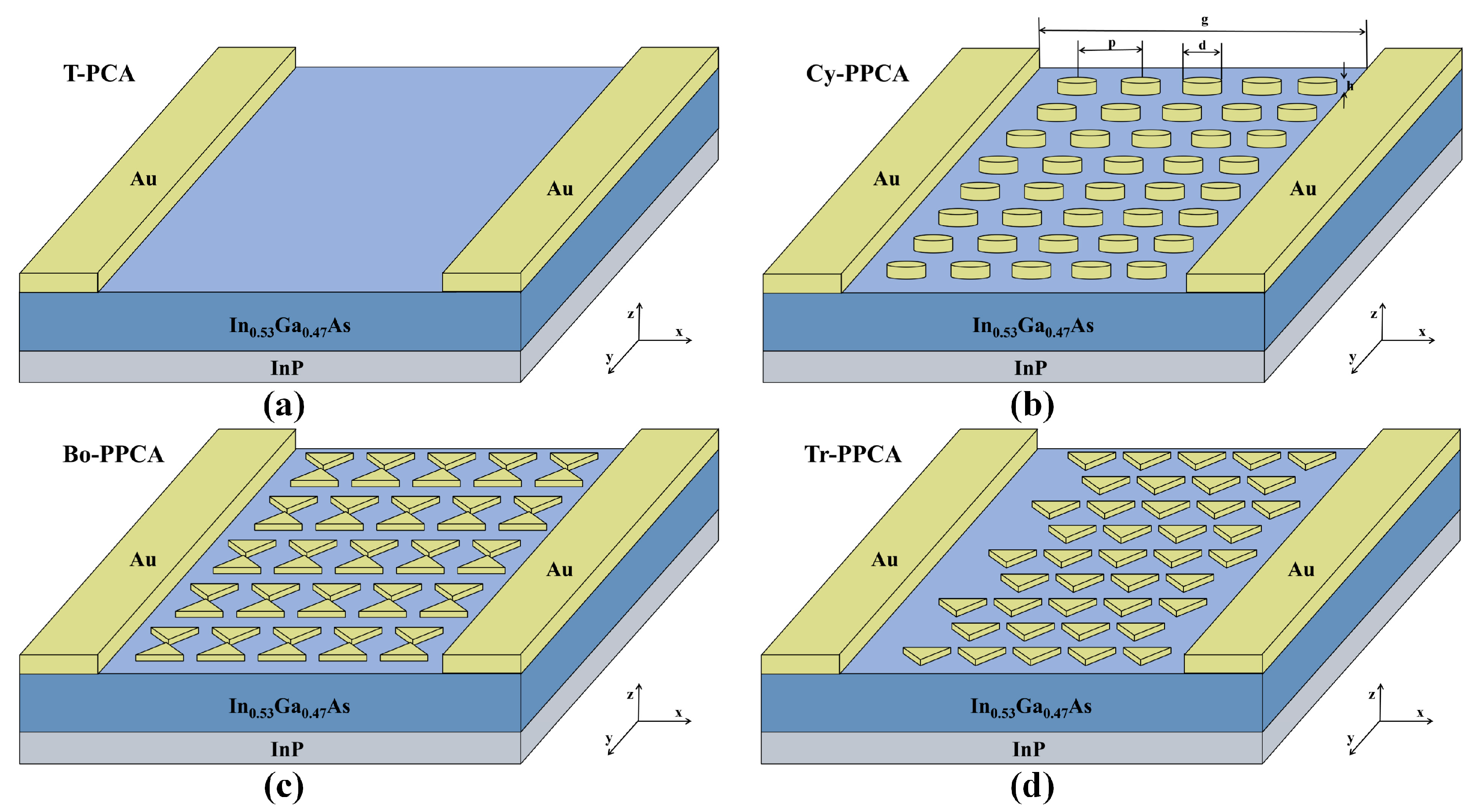
The overall structures of the photoconductive antenna with traditional structure (T-PCA) and the plasmonic photoconductive antenna with cylindrical nanoarray structure (Cy-PPCA), bowtie nanoarray structure (Bo-PPCA) and triangular nanoarray structure (Tr-PPCA) are shown in
Figure 1a–d, respectively. In all structures, the metal layers on the left and right of InGaAs semiconductor surface serve as the anode and cathode electrodes, separated by a 16 μm gap, while forming an ohmic contact with the underlying InGaAs layer. In Cy-PPCA emitters, periodic metal cylinder arrays can excite the localized surface plasmons in the gaps between electrodes. The conservation of energy and momentum between the surface plasmons and incident waves must be satisfied when the electromagnetic wave is optimally coupled to the metal nanoarray [
27]. The relationships between the propagation constant of the surface plasmon and plane wave vector of light in the medium should satisfy the following equations:
where
β is the surface plasmons wave vector,
θ is the incident electromagnetic wave angle with the surface,
ν is the mode number,
g is the nanostructure wave vector,
α is the periodicity of the nanostructure array,
ε1 is the relative permittivity of dielectric and
ε2 is the relative permittivity of metal. Assuming that the laser is incident vertically from directly above (
θ = 0) and first-order mode (
ν = 1) are satisfied, the period
α of the plasmonic nanoarray structure should satisfy [
28]
Furthermore, the thickness of the metal layer and the gap size has a significant impact on the excitation of surface plasmons and the field enhancement effect. For an excitation wavelength of 1550 nm, the emitter with optimized parameters of 50 nm height, 260 nm diameter and 290 nm periodicity achieved high absorption efficiency of 72.7% in the InGaAs layer.
The parameters of the femtosecond laser and some electrical parameters of the In
0.53Ga
0.47As layer are given in
Table 1. The femtosecond pulse laser beam with a Gaussian profile is normally incident on the center of the gap between the two electrodes. The beam has a spot size of 1 mm in diameter, ensuring uniform illumination across the electrode gap region, with its center positioned at (X
0, Y
0) = 2 μm relative to the simulated structure’s coordinate system. The optical response is calculated by defining a periodic boundary condition on the x-z boundary, and the absorbing impedance is assumed to match the boundary on the other surfaces.
When the femtosecond pulse laser is irradiated on the emitter, a self-induced electric field in the opposite direction of the biased electric field is generated due to the spatial separation of the electrons and holes, which causes the biased electric field to be shielded. Considering the existence of the electric field shielding effect, the expression of photocurrent density in the unit cell can be approximated as follows:
where
e and
μe are the charge and mobility of the electron, respectively.
n(
t) and
Ebias are the carrier density generated in each unit cell and the bias electric field, respectively. The total current density generated in the plasmonic PCAs is the sum of the current densities generated in all cells. Using the point-dipole model [
26], the electric field caused by polarization can be expressed as
where
η1 is a factor accounting for the geometry of the field in the active region and
κ is a shielding factor. In In
0.53Ga
0.47As, the peak carrier drift velocity reaches 2 × 10
7 cm/s, yielding a maximum travel distance
d of 200 nm inside the semiconductor [
29]. This corresponds to a calculated
η1max value of 3.47 × 10
−6. Here, the polarization P(t) denotes the macroscopic polarization resulting from spatial separation of photogenerated carriers (electrons and holes), which gives rise to the space-charge shielding field. The induced polarization resulting from carrier space-charge shielding can be derived by solving the rate equation:
As can be observed from Equation (7), the generation of polarization is a consequence of the displacement of carriers moving into the contacts to generate photocurrent, while the decay of polarization is caused by the recombination of carriers (
τR). To accurately simulate the space-charge shielding effect, this study defines the time-varying polarization intensity P(t) as a dependent variable in COMSOL Multiphysics 6.1 and solves its governing equation (Equation (7)), while the photocurrent density j(t) is computed in real time using Equation (5). P(t) is then incorporated into the Maxwell’s equations implemented in the transient electromagnetic wave interface. This bidirectionally coupled scheme dynamically captures the full physical process: the photocurrent drives polarization, which produces a shielding electric field that in turn influences carrier transport. This approach enables precise calculation of the shielding voltage. Distinct from the prevalent equivalent circuit model approach [
30,
31], this study employs a finite element method-based research strategy. Its significance extends beyond photoconductive emitters, where space-charge shielding effects are often inadequately addressed in conventional models. This method approach holds the potential to refine existing models and enable dynamic numerical simulations of the space-charge shielding voltage. Moreover, it facilitates detailed analysis of carrier distributions within the emitters, representing a notable advancement in the field.
3. Results and Discussion
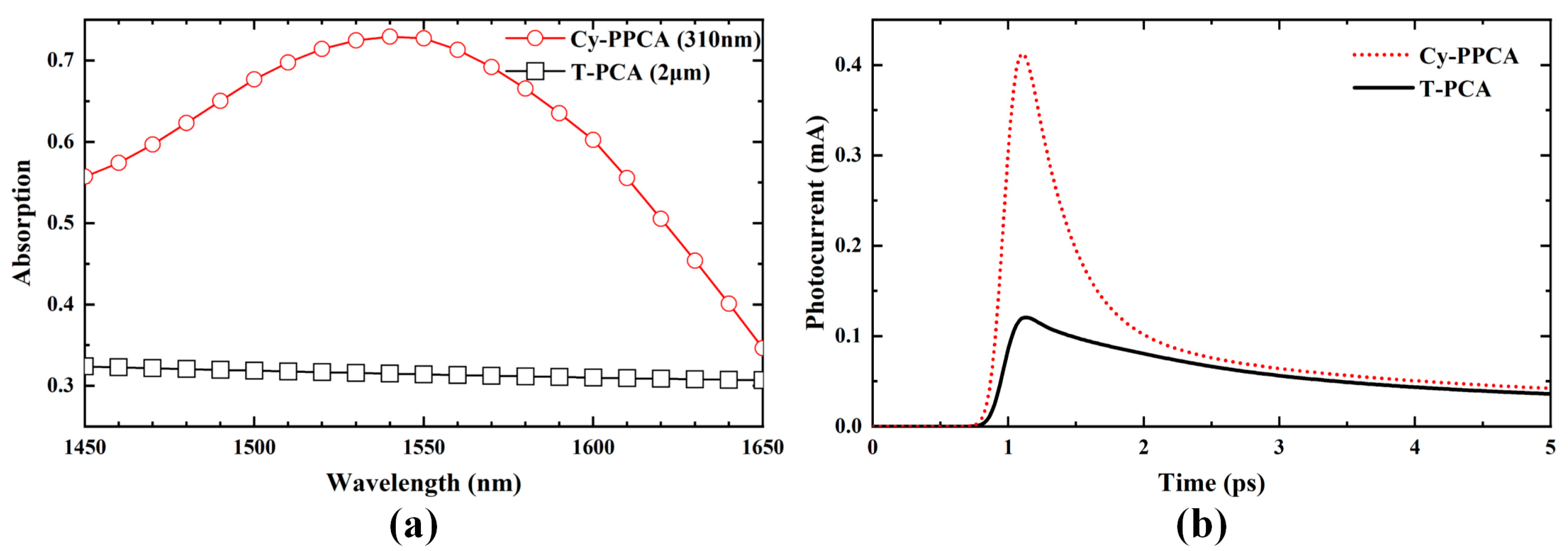
Figure 2a presents the absorption spectra of the InGaAs semiconductor layers in Cy-PPCA and T-PCA, with thicknesses of 310 nm and 2 μm, respectively. At the 1550 nm wavelength, an optical absorption rate of 72.7% was achieved for the Cy-PPCA emitter, significantly higher than the 31.4% observed for the T-PCA emitter. Leveraging the localized light field enhancement induced by plasmonic resonance, the nanoarray-based PCA significantly enhances light absorption within the photoconductive layer. This enables the 310 nm thick In
0.53Ga
0.47As layer to absorb over 70% of incident photons. It indicates that the plasmonic effect localizes the electric field within the electrode gap region, enabling effective absorption and conversion of more photons into charge carriers. Consequently, this leads to a comprehensive improvement in optical-to-THz conversion efficiency. In contrast, the overall light utilization efficiency of the T-PCA with thick InGaAs layer remains very low. As illustrated in
Figure 2b, the instantaneous photocurrent variation between the electrodes in the Cy-PPCA and T-PCA emitters is demonstrated. The photocurrents start to rise at around 1 ps, corresponding to the pulse duration time of the femtosecond pulsed laser. When the incident pulse laser illuminates into the photoconductor layer, the number of photogenerated carriers increases and moves rapidly to the electrodes in response to the electric field induced by bias voltage, resulting in a rapidly increasing transient photocurrent. It is found that the pulsed photocurrent of the Cy-PPCA emitter is about 3.46 times higher than that of the traditional structure emitter. This enhancement stems from plasmonic effects excited by the metallic cylindrical array, which elevates the light absorption rate of the In
0.53Ga
0.47As layer beyond 70%, resulting in more photogenerated carriers being able to be collected by the electrodes. Simultaneously, the plasmonic effect enables photogenerated carrier absorption within thinner semiconductor layers. In contrast to strategies utilizing short-carrier-lifetime materials such as LT-GaAs for direct ultrafast response, this study employs In
0.53Ga
0.47As—a semiconductor with high mobility and long carrier lifetime—to achieve high photocurrent. To overcome the transit time limitation inherent to such long-lifetime materials, plasmonic nanoarrays are incorporated to confine carrier transport to nanoscale distances. The plasmonic resonance spatially confines both optical energy and carrier generation to a surface-proximal nanolayer, significantly shortening the vertical transport distance. Concurrently, the localized fields around each nanoelement form guided channels that direct photogenerated carriers toward collection points, suppressing random drift and reducing the effective lateral transport path. This configuration shortens both the vertical and lateral carrier transport distances, thereby generating a stronger photocurrent within a shorter time interval. Consistently, the faster photocurrent decay observed in the falling edge of the time-domain spectrum directly results from the thin carrier generation region in plasmonic emitters, which minimizes vertical carrier travel distance and achieves an ultrafast response.
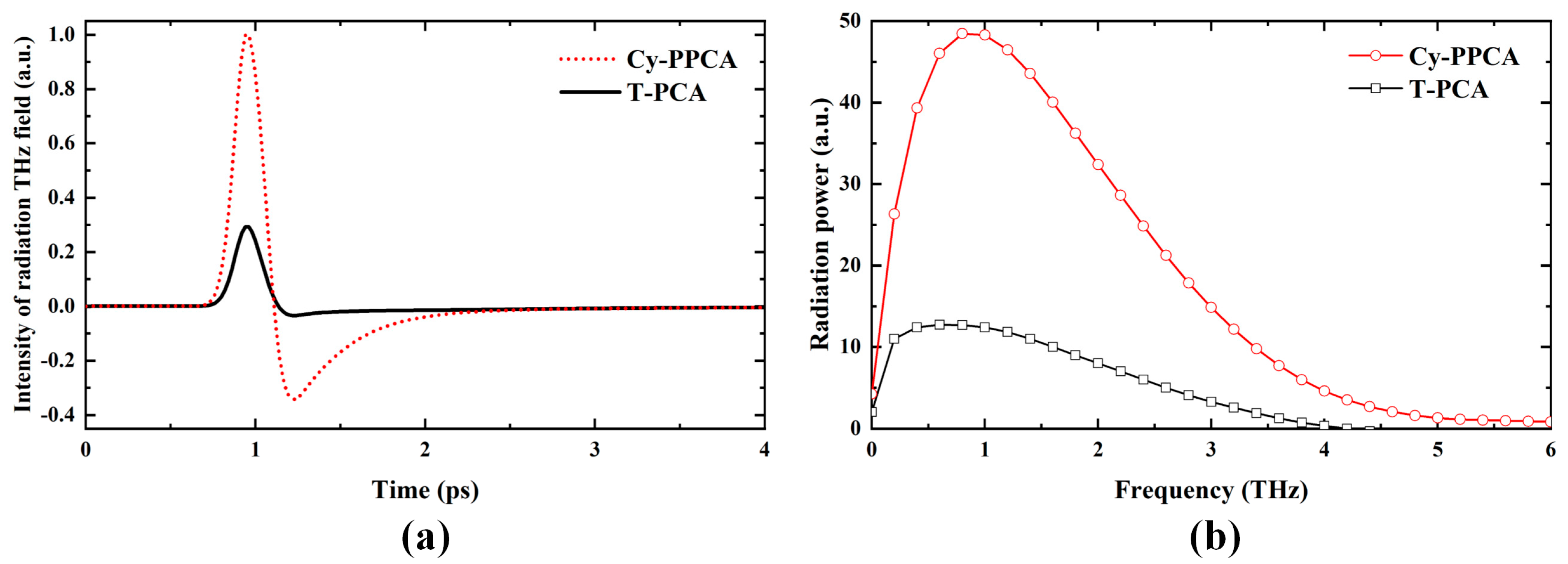
Figure 3a shows the THz radiation field spectra of the Cy-PPCA and T-PCA emitters. It is found that the intensity of the radiation field for the emitter with the plasmonic nanoarray is significantly enhanced as compared to that with the traditional structure, obtaining a 3.42-fold enhancement in THz field intensity at the peak position. The excitation of surface plasmon results in a considerable enhancement of the electromagnetic field strength at the emitter surface and the adjacent region, thereby markedly increasing the radiated field strength.
Figure 3b presents the radiation power spectrum obtained via fast Fourier transform of the field strength. The results indicate that the maximum radiation power for the T-PCA and Cy-PPCA emitters occurs at approximately 0.6 THz and 0.8 THz, respectively. Compared with the T-PCA emitter, the radiation power of the Cy-PPCA emitter is enhanced by 3.81 times. Moreover, the nanoarray structure emitters achieve a 5.5 THz bandwidth, representing a 50% increase over that of the traditional devices. Notably, the observed enhancement factor of the radiated power falls short of the ideal quadratic dependence on the peak photocurrent. This discrepancy arises because the total radiated power is integrated over the entire frequency range and is not only determined by its peak value. As a result, the actual enhancement factor remains lower than that predicted by squaring the peak current enhancement.
Table 2 summarizes the radiation bandwidth and field enhancement factors reported for various plasmonic PCAs under pulsed excitation conditions. The performance improvement demonstrated in this work is attributed to the enhanced light confinement, which significantly concentrates photogenerated carriers within the active region and shortens their transport distance. This results in faster decay rates for the photocurrent and contributes more high-frequency components to the overall radiation spectrum. Consequently, accelerated carrier collection at the electrodes produces both higher radiation power and broader bandwidth.
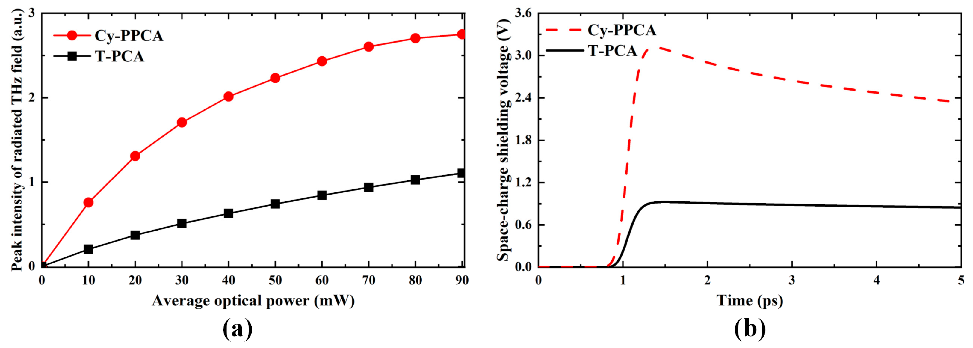
Figure 4a presents the peak THz radiation field strength of the T-PCA and Cy-PPCA emitters as functions of incident optical power. Owing to its higher carrier concentration and shorter carrier transport distance, the Cy-PPCA consistently outperforms the T-PCA in radiation field strength at identical incident power. However, the peak intensity of the radiation field of the plasmonic excitation structure has already shown a clear saturation trend when the incident laser power reaches 80 mW. At high optical pump power, the sharp rise in photogenerated carrier density significantly amplifies the space-charge shielding voltage. The resulting shielding field strongly counteracts the applied bias electric field, leading to saturation of the THz radiation. This saturation behavior is primarily caused by the space-charge shielding effect, rather than by an intrinsic limitation in the number of photogenerated carriers. Based on the Equations (5)–(7) described above, the shielding electric field strength as a function of time for both structures at a bias voltage of 20 V were calculated (see in
Figure 4b). The results indicate that the shielding voltage in the Cy-PPCA peaks at 3.1 V around 1.3 ps, which is 3.3 times higher than that of the T-PCA (0.93 V). The high carrier density generated in the Cy-PPCA promotes aggregation, yielding a substantially higher space-charge shielding voltage compared to the T-PCA. This intensifies the space-charge shielding effect, leading to radiation power saturation and directly affecting the electrical performance of the emitter. Notably, the bias voltage is critical in this process. In fact, increasing it exacerbates the shielding effect: a stronger bias field accelerates more carriers, resulting in more pronounced charge separation, which in turn induces a stronger space-charge shielding field. It is within this context that the plasmonic nanoarrays are designed primarily to enhance optical absorption and guide carrier transport. While the metallic nanostructures inevitably perturb the local bias field, a detailed quantification of this specific perturbation and its impact on breakdown behavior lies beyond the scope of this study and represents a valuable direction for future work.
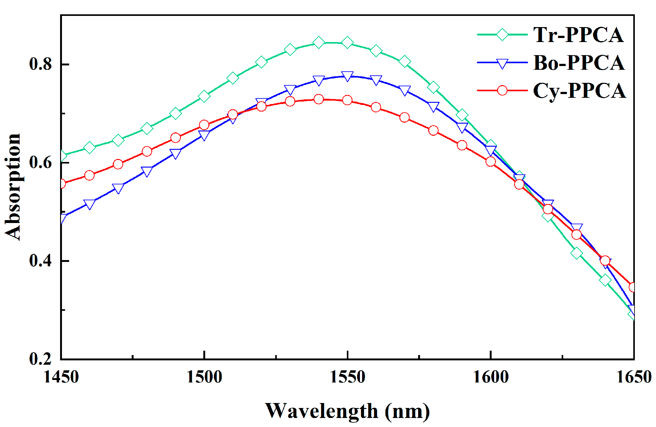
In order to reduce the space-charge shielding voltage and decrease the influence of the saturation effect, two other nanoarray structures were designed: the Bo-PPCA and Tr-PPCA. The nanoarray period (290 nm) and height (50 nm) were maintained identical to those of the cylindrical array to ensure uniform plasmonic resonance conditions. Furthermore, the size optimization ensures similar optical absorption at 1550 nm in each plasmonic nanoarray photoconductive emitter, as shown in
Figure 5. With the bowtie nanoarray featuring an arm length and adjacent gap of 240 nm and 20 nm, respectively, and the triangular nanoarray possessing a side length and tip-to-tip distance of 240 nm and 20 nm, respectively, both structures maintain strong absorption, preserving their radiation performance. Optimal performance demands high nanoarray uniformity to enable cooperative plasmonic resonance at the target wavelength, producing a sharp and intense resonance peak essential for maximizing field enhancement and THz output. In contrast, the maximum radiation frequency (bandwidth) depends mainly on the intrinsic carrier transit time to the nearest electrode, which remains largely unaffected by moderate structural variations.
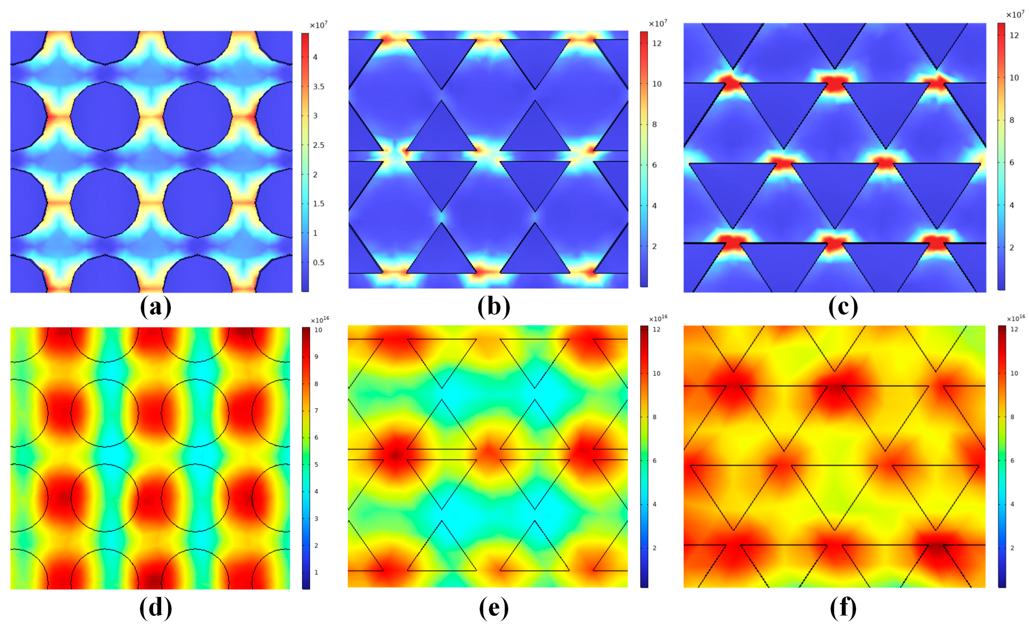
Figure 6a–c show the electric field distributions of the Cy-PPCA, Bo-PPCA and Tr-PPCA emitters at the wavelength of 1550 nm. The Tr-PPCA exhibits pronounced field localization at its triangular tips, forming distinct electric field hotspots. This nanoscale field concentration is attributed to the lightning-rod effect [
32] at the sharp tips, which promotes localized electron accumulation in the metal. Carrier aggregation occurs along the edges of the tip corners, resulting in increased drift current densities under bias conditions. Consequently, the charge density generated by the initial photogenerated carriers is concentrated near the surface of the device. The extremely strong local field enhancement near the sharp corners can facilitate the generation of additional carriers.
Figure 6d–f present the surface carrier distributions of the three nanoarray emitters under 1550 nm excitation conditions. The Tr-PPCA shows pronounced carrier accumulation along the triangular tip edges, spatially coinciding with the electric field hotspots. This correlation indicates that the enhanced local fields not only promote carrier generation but also guide their directional transport. Macroscopically, the Tr-PPCA establishes uniformly distributed excitation sites across the electrode gap, leading to an exceptionally homogeneous carrier profile that effectively suppresses random diffusion and localized accumulation.
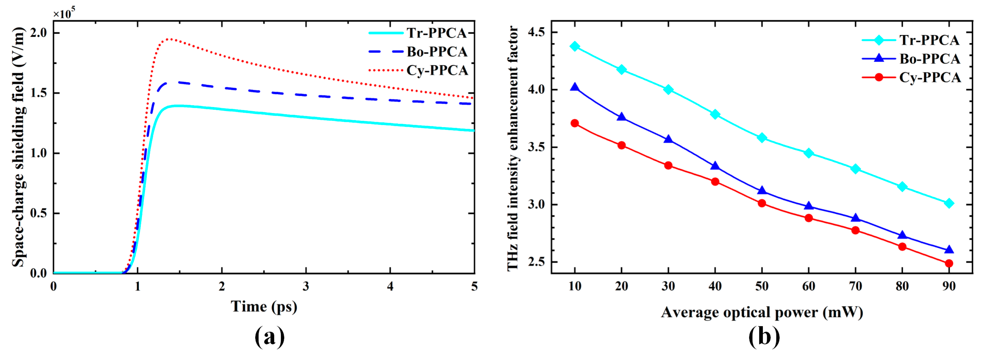
Figure 7a illustrates the space-charge shielding field intensities for the plasmonic nanoarray emitters with different nanoarray structures. The results show that the shielding electric fields strengthen progressively in all structures due to localized charge accumulation. Subsequent recombination of the uncollected carriers induces gradual field decay. The peak shielding field of the Tr-PPCA exhibits 28.72% and 12.65% reductions relative to Cy-PPCA and Bo-PPCA emitters at 1.3 ps, respectively. The Tr-PPCA substantially enhances electric field uniformity and carrier distribution homogeneity across the electrode gap. This effectively reduces localized charge accumulation, yielding lower average shielding field strength.
Figure 7b shows the radiated THz field enhancements of the plasmonic nanoarray emitters relative to that of the T-PCA at a 20 V bias voltage at varying average laser powers. As the laser power increases, the field enhancement factor decreases for all plasmonic emitters, indicating that the PCAs experience saturation under high-power conditions, attributed to the shielding effect. Notably, the Tr-PPCA with a uniform carrier distribution exhibits the least reduction in radiated field enhancement as the average laser power increases. At 90 mW, its radiation field intensity was 1.21 and 1.16 times that of the Cy-PPCA and Bo-PPCA, respectively, 1.16 and 1.08 times larger than at 10 mW. This indicates that the saturation effect impacts this structure less, providing additional evidence that its space-charge shielding effect is weakened.
