Article

Ultra-High Voltage NV Center Magnetic Sensing System Based on Power over Fiber

1
Laboratory of Optoelectronics and Sensor (OES Lab), School of Science, Hubei University of Technology, Wuhan 430068, China
2
School of Optical and Electronics Information, Huazhong University of Science and Technology, Wuhan 430074, China
3
State Grid Anhui Electric Power Company Ultrahigh Voltage Branch, Hefei 230000, China
4
School of Marxism, Hubei University, Wuhan 430062, China
*
Authors to whom correspondence should be addressed.
Photonics 2025, 12(11), 1093; https://doi.org/10.3390/photonics12111093
Submission received: 28 September 2025 / Revised: 31 October 2025 / Accepted: 4 November 2025 / Published: 6 November 2025

Abstract

Aiming to address the insulation and power supply challenges faced by electrical measurement in ultra-high voltage (UHV) environments, this study proposes and implements a nitrogen-vacancy (NV) center magnetic sensing system based on Power over Fiber (PoF) technology. The system adopts a high-voltage and low-voltage separation design, realizing the isolated transmission of electrical energy and the reliable recovery of measurement signals through an optical fiber link. The sensing unit on the high-voltage side is composed of NV center sensors, microwave excitation modules, and signal processing modules. Its power supply is provided by an independently developed high-power laser power converter (LPC) assembly via 830 nm optical fiber laser transmission. Under an optical input of 10 W, this assembly can achieve an electrical output of 4.88 W with a conversion efficiency of 48.9%. The experimental results show that the system can operate stably in a simulated UHV environment; by optimizing modulation parameters, the optimal magnetic measurement sensitivity reaches 6.1 nT/Hz1/2. This research provides a safe and reliable solution for the power supply and precise sensing of high-potential side equipment in UHV scenarios, and demonstrates the application potential of PoF technology in advanced sensing for power systems.

1. Introduction

Nitrogen-vacancy (NV) centers, as atomic-scale defects in diamond, have emerged as one of the most promising platforms in the field of quantum sensing, thanks to their excellent optical polarization and spin readout properties at room temperature [1,2,3]. Based on the Optically Detected Magnetic Resonance (ODMR) technique, NV center sensors enable magnetic field measurements with nanoscale spatial resolution and nanotesla-level sensitivity, providing revolutionary measurement tools for fields such as biomedical imaging [4], fundamental physics research [5], and industrial non-destructive testing [6].
In recent years, with the rapid development of ultra-high voltage (UHV) power transmission technology, higher requirements have been put forward for the condition monitoring of electrical equipment. Leveraging advantages such as non-contact measurement, a wide dynamic range, and resistance to electromagnetic interference, NV center sensing technology has shown great potential in the field of UHV current monitoring [7,8,9]. Compared with traditional electromagnetic transformers, quantum-effect-based NV sensors are free from magnetic saturation issues. They are expected to achieve accurate current measurement across a frequency range from direct current (DC) to kilohertz, offering a next-generation measurement solution for smart grids [10,11].
However, the application of NV center technology in UHV environments faces a fundamental challenge: the reliable power supply for sensing units on the high-potential side. The electric field intensity in UHV environments can reach several megavolts per meter; the introduction of any metal wires will lead to insulation failure and severe electromagnetic interference [12,13]. This bottleneck has seriously restricted the promotion and application of NV center technology in power systems.
Power over Fiber (PoF) technology, which transmits optical energy remotely via optical fibers and converts it into electrical energy on the high-voltage side using a laser power converter (LPC), provides an ideal solution to this problem [14,15]. Utilizing the excellent electrical insulation properties of optical fibers themselves, this technology completely isolates high and low potentials, fundamentally ensuring the safety and reliability of the system [16]. In particular, the development of multi-junction GaAs-based LPC technology in recent years has made it possible to break through the 50% photoelectric conversion efficiency threshold, providing sufficient power support for UHV sensing systems [17,18].
Despite the obvious advantages of PoF technology, research on dedicated LPCs for UHV NV center sensing systems still faces the following challenges: (1) existing commercial photovoltaic cells cannot simultaneously meet the requirements of high-power output and high conversion efficiency; (2) extreme temperature variations (−30 °C to 70 °C) in UHV environments pose severe challenges to the performance stability of LPCs; and (3) NV sensing systems have extremely high requirements for power supply quality (including noise and stability), which traditional LPCs struggle to meet [19,20].
To address the above challenges, this study successfully constructed an all-fiber NV center magnetic sensing system for UHV applications by designing and fabricating a high-efficiency six-junction GaAs-based LPC. Compared with previously reported PoF-powered sensing systems [21,22], the core novelty of this work lies in the design and implementation of a high-performance, high-efficiency, and full-temperature-range stable LPC module specifically for NV center quantum sensing systems in UHV environments, as well as the successful construction of a complete, all-fiber-isolated four-channel PoF-NV magnetic sensing system, resolving the core contradiction of power supply and insulation on the high-potential side. In the research, we systematically evaluated the performance of the LPC under extreme temperatures ranging from −30 °C to 70 °C to ensure the stability of its power supply. Finally, through system integration and testing, an actual measurement sensitivity of 6.1 nT/Hz1/2 was achieved in a simulated UHV environment, and a comparison was made with recently reported NV-center-based magnetic sensing systems, providing a practical solution to the power supply problem of equipment on the high-potential side.
Section 2 of this paper introduces the system principle and LPC assembly design; Section 3 presents the experimental test results; Section 4 discusses system performance, parameter optimization, and a comparison with typical magnetic sensing systems based on NV center technology; Section 5 summarizes the entire study and outlines future work.

2. Materials and Methods

2.1. A UHV NV Center Magnetic Sensing System

To achieve insulated and reliable measurement in UHV environments, the system adopts a high-voltage and low-voltage separation design, with its specific structure shown in Figure 1. The system is divided into a high-voltage side and a low-voltage side, connected via optical fiber links.
The high-voltage-side module comprises NV center sensors and a remote module. The remote module integrates a radio frequency (RF) microwave source, a circulator (CIR), a low-noise amplifier (LNA), a lock-in amplifier (LIA), a field-programmable gate array (FPGA) module, and a low-speed optical transmitter module. On the low-voltage side, the module consists of a 532 nm laser, a high-power laser (HPL), and a signal reception module.
During system operation, the 532 nm laser and modulated GHz microwave act together on the NV center sensors to excite their fluorescence signals. After LIA and FPGA demodulation, these signals are transmitted to the low-voltage side via an 850 nm multi-mode fiber (MMF) for signal processing and magnetic field information reconstruction. The CIR is designed to prevent microwave backpropagation from damaging the microwave source module, while the low-noise amplifier amplifies the power of the GHz microwave and suppresses noise.
As measured, the power consumption of each component on the high-voltage side is analyzed in Table 1, with a total power consumption of approximately 3.8 W. In practice, due to power conversion (DC–DC) efficiency and load variations, the required power is higher. Therefore, a high-power LPC based on PoF technology becomes a key solution to address this power supply challenge.

2.2. Design of the LPC Assembly

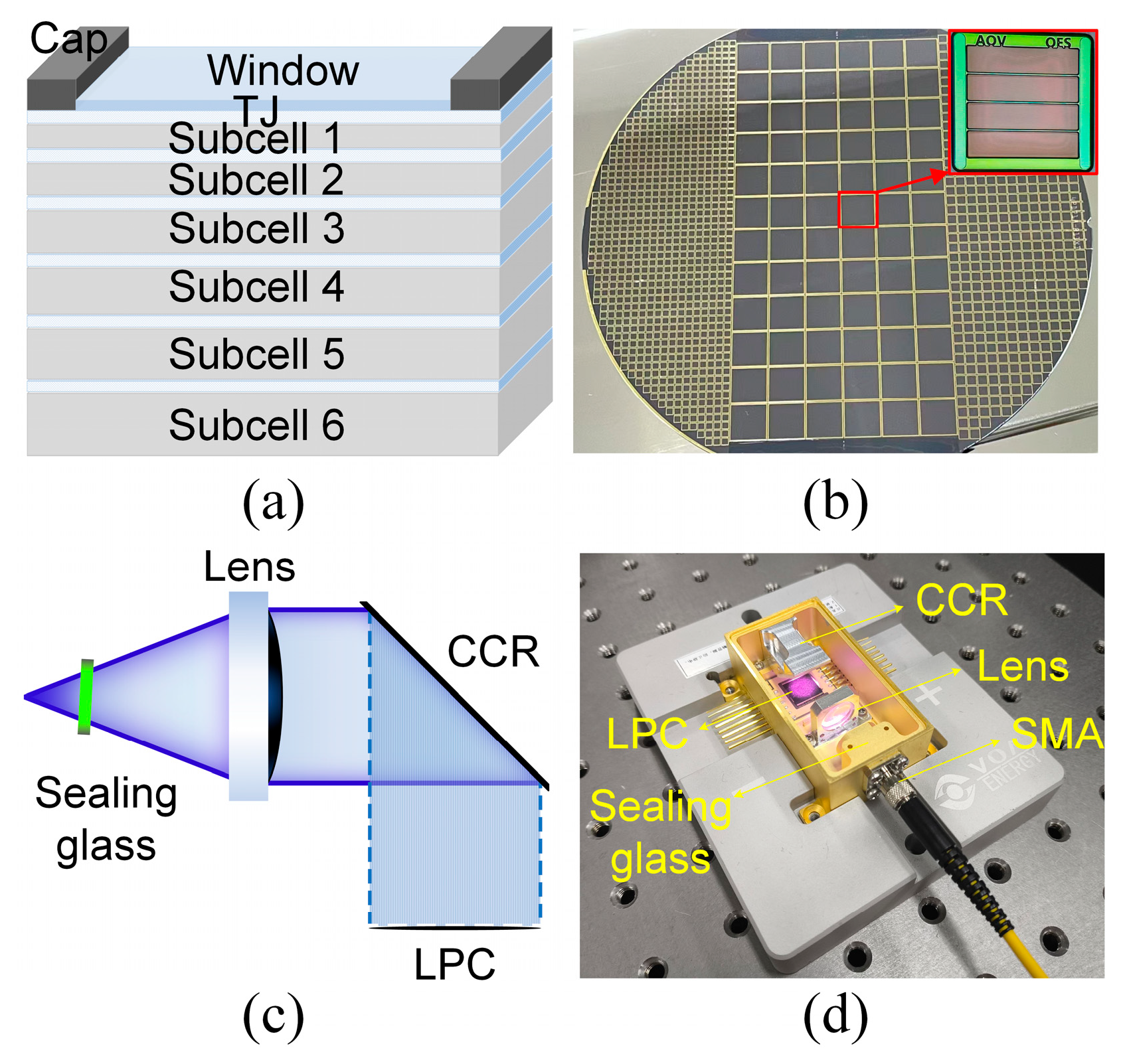
To meet the high-voltage power supply requirements of the NV center magnetic sensing system shown in Figure 1, a high-power LPC assembly was designed. The schematic diagram of the device chip is presented in Figure 2a, which includes 6 subcells with different thicknesses. To achieve optimized electrical properties in the multi-junction LPC, the top subcell is the thinnest while the bottom subcell is the thickest; each subcell is designed to generate the same photocurrent for current matching [23]. The subcells are interconnected in series via heavily doped tunnel junctions (TJs) to enhance carrier mobility, and the total output voltage of the converter equals the sum of the output voltages of the individual subcell.
In addition, the module includes a window layer made of a wide-bandgap material, which is transparent to the input light and primarily functions to reduce the recombination rate on the converter surface. Finally, an N-type electrode cap layer is grown on the window layer, serving as an ohmic contact to minimize contact resistance. A physical image of the wafer and a magnified view of the chip are shown in Figure 2b.
For high-power assemblies, achieving a larger and more uniform laser spot helps reduce energy density stress. Therefore, an aspheric lens is used to expand and collimate the incident laser beam, obtaining a larger uniform laser spot. Meanwhile, the distance between the heat sink and the assembly needs to be minimized to reduce thermal resistance. A semi-transparent and semi-reflective optical path structure was thus designed, as shown in Figure 2c. Using Zemax optical simulation software (2024 R2.02), the optimal optical structure was determined as follows: the aspheric lens has a focal length of 25 mm and a diameter of 10 mm; the corner cube retroreflector (CCR) has dimensions of 17 mm × 13 mm × 1.5 mm. Additionally, a 1 mm thick sealing glass tilted at 4° is used to prevent light reflection. The distance between the sealing glass and the center of the CCR is 19.7 mm, and the distance between the CCR and the LPC is 9.48 mm.
Figure 2d shows the internal view of the compact LPC assembly fabricated based on our patented assembly technology [24], with a designed size of 64 mm × 48 mm × 22 mm. In terms of power supply capacity design, sufficient redundancy reliability was considered for the system during actual operation. To cope with load fluctuations, temperature changes, and performance degradation during long-term operation, the asse is designed for a maximum output electrical power of 4.8 W. This redundant design ensures continuous stability and a safety margin for system power supply in complex UHV environments.

3. Results

3.1. Characteristic of LPC Component

An 830 nm laser (Aov: Compact Series 20 W, the threshold power 1 W) with an adjustable power range of 1–20 W was used as the monochromatic light source. The optimal I-V curve scanning method for GaAs LPCs [25] was adopted, with a pulsed light duration ranging from 10 ms to 1 s and an interval of 4 min. This interval is designed to avoid temperature-induced interference on the module, ensuring accurate testing of its photoelectric properties.
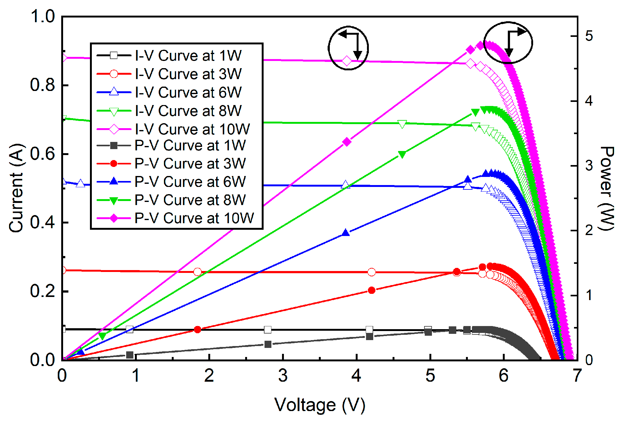
The I-V (current–voltage) and P-V (power–voltage) curves of the assembly were tested under different incident light powers, as shown in Figure 3. At a laser power of 1 W, the module achieved an output power of approximately 0.45 W, with a maximum power point voltage (Vpmax) of 5.62 V and a maximum power point current (Ipmax) of 0.08 A. Under this condition, the fill factor (FF) was 81.34% and the conversion efficiency was approximately 45%. When the laser power increased to 10 W, the output electrical power reached 4.88 W, with Vpmax and Ipmax of 5.75 V and 0.85 A, respectively. In this case, the FF was 80.14% and the efficiency was approximately 49%.
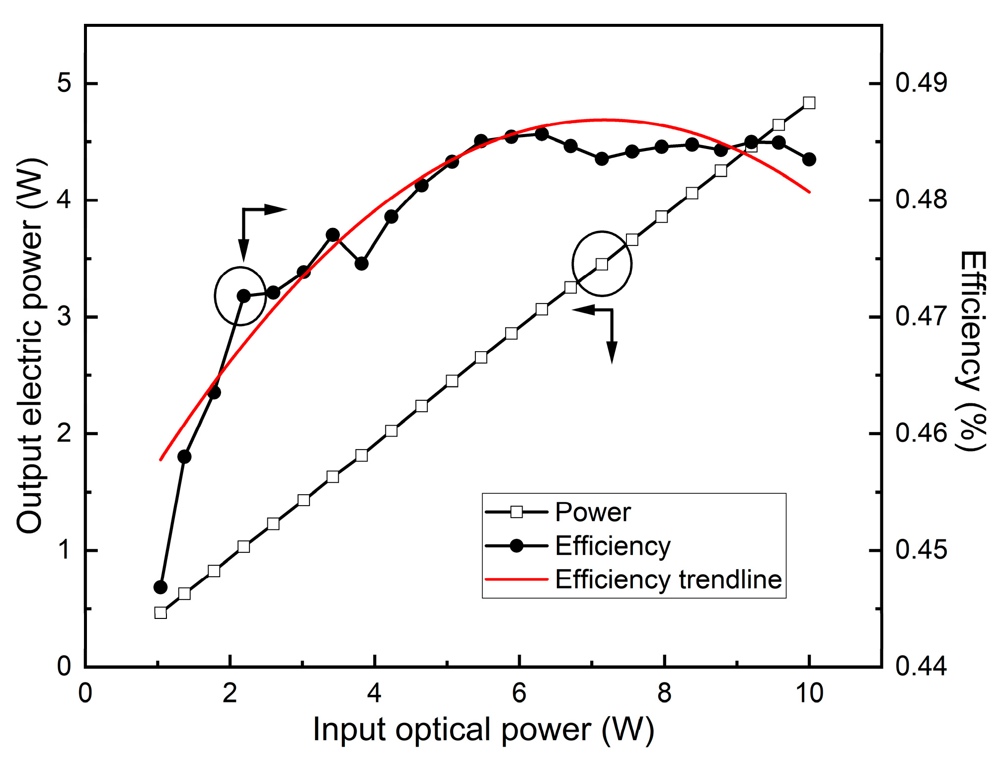
Additionally, the output characteristics of the fabricated assembly were tested individually under continuous light powers ranging from 1 to 10 W, as shown in Figure 4. When the laser power increased to 6.3 W, the assembly exhibited a maximum photon energy efficiency of 48.57%, corresponding to an open-circuit voltage (Voc) of 6.86 V and a short-circuit current (Isc) of 0.556 A. When the laser power further increased to 10 W, the output power was 4.84 W, and the efficiency slightly decreased to 48.35%. The efficiency–power curve first showed an increasing trend, followed by a decreasing trend (red curve). This result is mainly attributed to the influence of temperature on the performance characteristics of the LPC: temperature exerts a similar effect on voltage characteristics (since each subcell is made of the same material), but differs in its impact on current characteristics (primarily due to the varying thickness of each subcell). This ultimately leads to a non-linear variation in the efficiency–power curve. It can be observed that the laser power increases linearly (square curve); the corresponding relationship between the output electrical power and the incident laser power can be used to calibrate the intensity of the laser power.

3.2. System Application

The actual constructed UHV NV center magnetic sensing system physically constructed in this study is shown in Figure 5a. Under test conditions, the high-voltage side of the system mainly consists of three core components: a high-voltage bus, a sensing loop, and a remote module. The high-voltage bus can withstand a maximum DC voltage of 1200 kV, corresponding to an electric field intensity of approximately 640 kV/m, which simulates the real UHV operating environment. To ensure high-voltage insulation performance, a vacuum potting process is adopted between the sensing loop and the high-voltage bus: two-component soft silicone rubber is potted with composite insulators as the carrier, and this assembly serves as the main insulating medium to effectively avoid the risk of high-voltage breakdown. The NV center sensor is encapsulated inside the sensing loop, with its core function being real-time detection of magnetic field signals generated by the current in the high-voltage bus.
The sensor adopts a “optical input–electrical output” design architecture: one end receives 532 nm excitation laser, and the other end is connected to a radio frequency (RF) microwave signal; the final output electrical signal contains magnetic field information. The sensor is packaged in a compact form with an overall size not exceeding 33 mm × 24 mm × 5 mm, and is hermetically sealed in a nitrogen environment to improve long-term stability (Figure 5b).
The remote module (Figure 5c) serves as the core processing unit on the high-voltage side, integrating functional circuits such as an RF microwave source, lock-in amplification, FPGA signal demodulation and modulation. To achieve multi-directional magnetic field measurement, the system actually deploys 4 independent magnetic sensing channels, with a total power consumption of approximately 15.2 W on the high-voltage side. To enhance the reliability of the system’s power supply, a redundant backup strategy for LPC assemblies is adopted, using a total of 4 LPC assemblies connected in parallel to prevent system operation interruption caused by the failure of a single power supply unit. A simplified diagram of the overall system architecture is shown in Figure 5d.

3.3. System Performance

After DC–DC conversion, the LPC assembly provides an output electrical power of 3.8 W, which supports the normal operation of the high-voltage side system. With the microwave source frequency sweep range set to 2.85–2.89 GHz and the lock-in amplifier in DC mode, the ODMR spectrum of the NV center was plotted by reading the fluorescence intensity R value, as shown in Figure 6a(i). Under this condition, the excitation laser power was 25 mW and the microwave power was 15 dBm; the measured spectral contrast ratio (CR) was 2.46% and the full width at half maximum (FWHM) was 3.25 MHz.
The LIA was switched to alternating current (AC) mode to perform phase locking with the same-frequency sinusoidal reference signal emitted by the microwave source. After demodulation by the FPGA, a demodulation curve was obtained, as shown in Figure 6a(ii). Linear fitting and differentiation of this curve yielded the corresponding first-derivative response, as shown in Figure 6a(iii).
Within the frequency range of 10–100 Hz, the amplitude spectral density (ASD) of system was 0.875 μV/Hz1/2, with the ASD shown in Figure 6b. A significant peak was observed at 50 Hz, which originates from power grid frequency interference. Based on the ODMR principle, the magnetic field sensitivity η can be calculated using the following formula [26]:
η =   A S D k × γ e  
where γ e is the electron gyromagnetic ratio (approximately 28 Hz/nT) and k is the slope of the ODMR demodulation curve. Under this default operating mode, the long-term test results of the system sensitivity are shown in Figure 6c, where both the ASD and demodulation slope are averaged over 10 measurements. The maximum sensitivity is 13.74 nT/Hz1/2, and the minimum is 9.2 nT/Hz1/2. Sensitivity shows an increasing trend during the continuous test (red trend line). The degradation of sensitivity η is directly related to the increase in sensor temperature. As shown in Formula (1), η    ASD/k. As the sensor temperature rises due to continuous laser irradiation (we did not implement active temperature control in the experiment), the spin coherence time T2 of NV centers will shorten. This leads to broadening of the ODMR spectrum and reduced signal-to-noise ratio. According to our data and existing literature [27], T2 is highly temperature-sensitive, where for every 10 °C increase above room temperature, T2 may decrease by approximately 20%. This degradation of coherence is the main reason for the time-dependent decrease in sensitivity. It is worth noting that under the optimized modulation parameters described in Section 4.2, the system can achieve a best sensitivity of 6.1 nT/Hz1/2.

4. Discussion

4.1. Full Temperature Operating Characteristics of the LPC Assembly

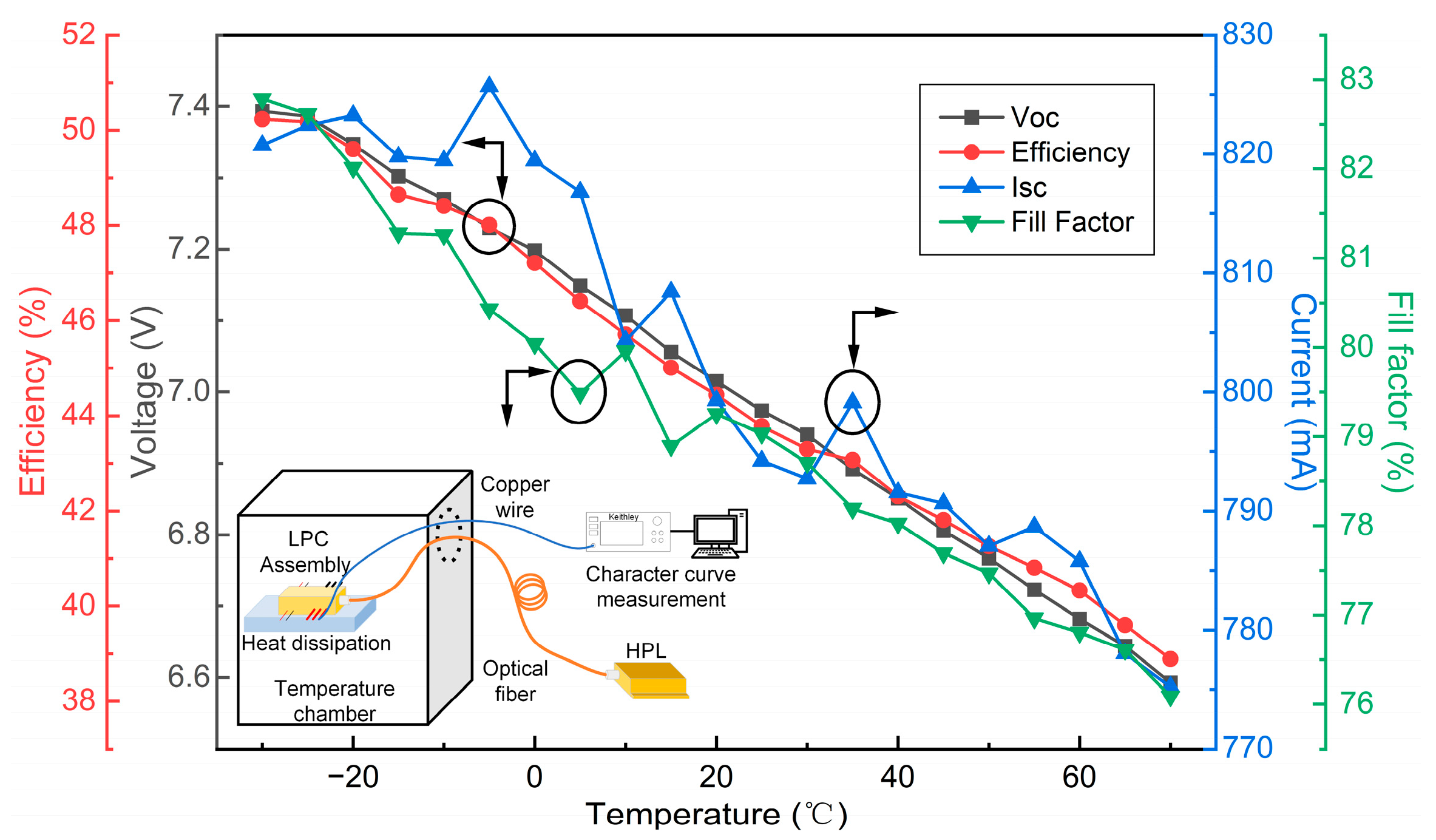
To evaluate the applicability of the developed LPC assembly in actual UHV environments, its operating characteristics under full temperature conditions were systematically investigated. UHV equipment operates within a wide temperature range, and the LPC assembly may be exposed to long-term working conditions of −30 °C to 70 °C; thus, the reliability of its performance across the full temperature range is critical.
A full temperature aging chamber was used to characterize the performance of the assembly. This device allows precise control and programmed ramp changes of the ambient temperature. During the test, the LPC assembly and its supporting heat sink were placed in a temperature-controlled chamber, and electrode leads were connected to an external measurement unit via feedthrough interfaces to monitor electrical parameters in real time. The test procedure was as follows: first, the chamber temperature was stabilized at −30 °C; after the module temperature and output electrical parameters reached a steady state, the power–current–voltage (PIV) characteristic curve at this temperature was recorded. Subsequently, the chamber temperature was gradually increased, and the above measurement process was repeated at each set temperature point (e.g., −20 °C, −10 °C, 0 °C, 10 °C, up to 70 °C) to ensure data continuity and comparability.
Figure 7 shows a simplified schematic of the experimental setup and typical test results. The experimental results clearly indicate that as the ambient temperature increases, the photoelectric conversion performance of the LPC assembly exhibits a regular change: the open-circuit voltage (Voc), short-circuit current (Isc), photoelectric conversion efficiency, and fill factor (FF) all decrease. Specifically, the Voc of the assembly exhibits a significant negative temperature coefficient, decreasing by approximately 11.5 mV per degree Celsius on average. The conversion efficiency and maximum output power also decrease monotonically with increasing temperature, with the temperature coefficient of output power being approximately −0.31%/°C. This phenomenon is mainly attributed to the fundamental properties of semiconductor materials: increased temperature leads to a rise in intrinsic carrier concentration, a decrease in carrier mobility, and a reduction in the built-in potential of the PN junction—all of which collectively cause the decline in Voc and FF. Although Isc may increase slightly due to bandgap narrowing, this effect is insufficient to offset the dominant impact of voltage attenuation, ultimately resulting in a decrease in conversion efficiency. These research results provide key data support for the thermal management design and output power calibration of the LPC in UHV environments, and are of great significance for ensuring the long-term stable operation of the entire magnetic sensing system under complex working conditions.

4.2. Sensitivity Optimization of the NV Center Sensor

To achieve the optimal performance of the NV center magnetic sensing system based on PoF, this study conducted collaborative optimization of the key parameters affecting its sensitivity, namely 532 nm laser power and microwave power. Under the PoF architecture adopted in this system, the power supply for modules such as the microwave source on the high-voltage side comes from the stable output of the LPC assembly. This power supply method ensures the controllability and stability of microwave power, laying a foundation for system sensitivity optimization.
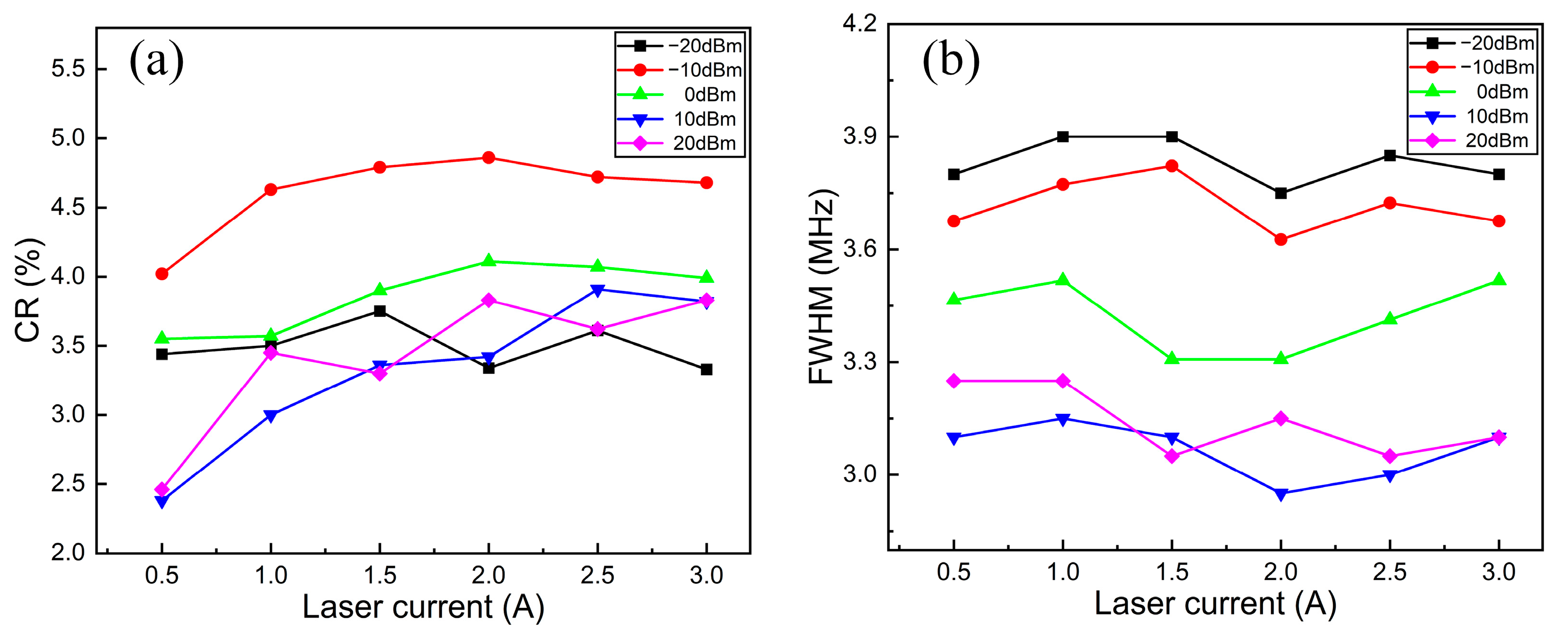
Under the condition of an applied axial pre-biased magnetic field, the energy levels of NV centers undergo Zeeman splitting, allowing the observation of a typical double-peak ODMR spectrum. In the experiment, ODMR signals were collected under combinations of different microwave powers (−20, −10, 0, 10, 20 dBm) and laser powers (adjusted via a drive current of 0.5 A to 3.0 A, corresponding to a light intensity of approximately 5 mW to 80 mW). The left resonance peak was uniformly selected for quantitative analysis.
The results in Figure 8a show that within a certain range, the FWHM of the spectral line is mainly regulated by microwave power: higher microwave power helps to obtain a narrower linewidth. With increasing laser power, the FWHM shows a non-monotonic trend of first increasing and then decreasing. Figure 8b indicates that the spectral CR first increases and then decreases with increasing laser power, and generally exhibits higher contrast when the microwave power is −10 dBm. The above parameters collectively determine the theoretical sensitivity limit of the system η t h , whose expression is:
η t h = 4 3 3 g e μ B Δ ν C R
where 4 3 3 is the Lorentz fitting line shape parameter, Δ ν is the linewidth, C is the contrast ratio, R is the photon count rate, g e ≈ 2.003 is the electron g-factor, and μ B is the Bohr magneton. Therefore, reducing the FWHM and increasing the CR are key approaches to improving sensitivity.
Experiments show that there is a clear optimal operating point for laser and microwave power in the system. When the microwave power is −10 dBm and the laser power is 50 mW, the η t h of the system can reach 0.1 nT/Hz1/2.
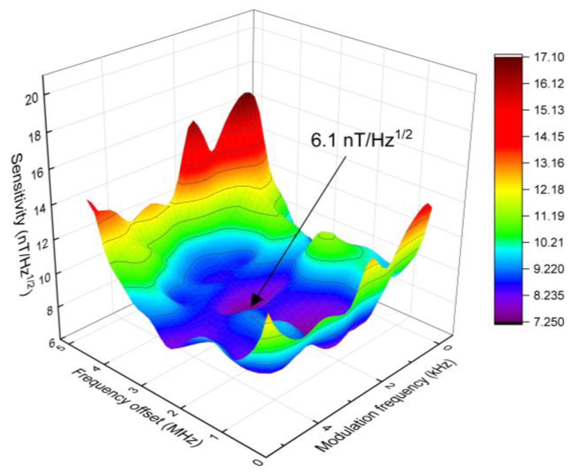
On the basis of theoretical optimization, experimental verification of modulation parameters (including modulation frequency and frequency offset) was further conducted. The frequency offset range was set to 0–5 MHz, and the modulation frequency was adjusted within 0.4–4.8 kHz. The measured results are shown in Figure 9. When the modulation frequency is 2.8 kHz and the frequency offset is 3 MHz, the system achieves the best actual sensitivity, reaching 6.1 nT/Hz1/2. The difference between this result and the theoretical value is mainly due to experimental environmental noise, temperature fluctuations, and additional losses during signal demodulation.

4.3. Performance Comparison and Analysis

To objectively evaluate the performance positioning and competitive advantages of this system among similar technologies, Table 2 systematically compares the key performance indicators of this study with recently reported typical magnetic sensing systems based on NV center technology. The comparison dimensions cover measured sensitivity, power supply mode, application scenarios, and core advantages/drawbacks.
Compared with other systems listed in the table that use local batteries or wired power supplies, this system applies high-power PoF technology to the NV center sensing system in UHV environments, achieving complete electrical isolation between the high-voltage and low-voltage sides. This enables the system to be directly applied to kV-level UHV scenarios where traditional electronic devices fail due to insulation issues and electromagnetic interference.
In terms of sensitivity, the 6.1 nT/Hz1/2 achieved by this system is lower than that of highly optimized laboratory systems (e.g., 2.25 nT/Hz1/2 in [28]), but significantly higher than most application-oriented solutions for industrial on-site use (e.g., [29,30,32]). More importantly, this sensitivity is achieved under the electromagnetic and temperature stresses of a simulated UHV environment, reflecting the system’s comprehensive usability under extreme operating conditions rather than merely a pure indicator of limit performance.
Compared with most studies that focus on probe miniaturization or circuit integration, this work not only emphasizes the sensing core but also completes full-system integration: it covers a dedicated high-efficiency LPC, multi-channel signal processing, and redundant power management. This advances NV quantum sensing from laboratory proof-of-concept to on-site applications in the power industry.

5. Conclusions

In this study, an NV center magnetic sensing system based on PoF technology was successfully designed and validated, providing an effective solution to address the power supply and signal isolation challenges of high-potential side sensing equipment in UHV environments. The key contributions of this research are summarized as follows:
First, a system architecture for high-voltage and low-voltage isolation based on an all-fiber link was proposed. This architecture enables the simultaneous transmission of electrical energy and recovery of signals via optical fibers, fundamentally avoiding the insulation issues caused by traditional metal wires and ensuring the operational safety and reliability of the system in UHV environments.
Second, a high-efficiency multi-junction LPC assembly was developed. Under 830 nm laser input, the module achieved a photoelectric conversion efficiency of up to 48.9% and a maximum output electrical power of 4.88 W. It also exhibited excellent environmental adaptability within the temperature range of −30 °C to 70 °C, with a temperature coefficient of output power of approximately −0.31%/°C, making it capable of stable power supply under complex UHV operating conditions.
Furthermore, a 4-channel NV center magnetic sensing system was integrated and experimentally verified. By optimizing the parameter matching between microwave power and laser power, and under the conditions of a modulation frequency of 2.8 kHz and a frequency offset of 3 MHz, the system achieved an optimal measured sensitivity of 6.1 nT/Hz1/2.
Although the system showed an upward trend in sensitivity during continuous testing—mainly due to the degradation of NV center coherence caused by increased sensor temperature—this finding points out directions for future thermal management design improvements. Overall, this research confirms the feasibility of applying PoF technology to high-precision magnetic sensing in UHV environments, providing a new technical pathway for electrical measurement in high-voltage, strong electromagnetic interference scenarios. Future work will focus on improving the high-temperature performance of LPCs, optimizing the thermal stability of sensors, and promoting the application of this technology in power internet of things (IoT) and new-type power system sensing.

Author Contributions

Conceptualization, L.Z. and C.G.; methodology, L.Z. and C.G.; software, L.Z.; validation, L.Z., X.F., W.W., Y.X. and X.C.; formal analysis, L.Z., C.D. and Q.G.; investigation, L.Z., C.D. and Q.G.; resources, J.H. and X.Z.; data curation, L.Z.; writing—original draft preparation, L.Z.; writing—review and editing, L.Z. and W.J.; supervision, C.G. and W.J.; funding acquisition, J.G. All authors have read and agreed to the published version of the manuscript.

Funding

Thanks for the support of the project “Ultra-high resolution optical fiber spectrum analyzer (2023YFF0715800)” supported by the OES Lab, School of Science, Hubei University of Technology, and the project “Research on Key Technologies for Improving Stability and Reliability of Optoelectronic CT Measurement in Ultra High Voltage Scenarios” (Project No.: 5700-202420251A-1-1-ZN) supported by State Grid Corporation of China, and the project “Research on High-Quality Autonomous Preparation and Application Technology of Diamond NV Centers” (Project No.: 2025BEA001) led by the National High Voltage Metrology Station. We also gratefully acknowledge the financial support from Wuhan AOV Energy LLC.

Institutional Review Board Statement

Not applicable.

Informed Consent Statement

Not applicable.

Data Availability Statement

The original contributions presented in this study are included in the article. Further inquiries can be directed to the corresponding author(s).

Conflicts of Interest

Xueyou Zhang was employed by State Grid Anhui Electric Power Company Ultrahigh Voltage Branch. The remaining authors declare that the research was conducted in the absence of any commercial or financial relationships that could be construed as a potential conflict of interest.

References

  1. Degen, C.L.; Reinhard, F.; Cappellaro, P. Quantum sensing. Rev. Mod. Phys. 2017, 89, 035002. [Google Scholar] [CrossRef]
  2. Schirhagl, R.; Chang, K.; Loretz, M.; Degen, C.L. Nitrogen-vacancy centers in diamond: Nanoscale sensors for physics and biology. Annu. Rev. Phys. Chem. 2014, 65, 83–105. [Google Scholar] [CrossRef]
  3. Rondin, L.; Tetienne, J.P.; Hingant, T.; Roch, J.-F.; Maletinsky, P.; Jacques, V. Magnetometry with nitrogen-vacancy defects in diamond. Rep. Prog. Phys. 2014, 77, 056503. [Google Scholar] [CrossRef]
  4. Webb, J.L.; Troise, L.; Hansen, N.W.; Achard, J.; Brinza, O.; Staacke, R.; Kieschnick, M.; Meijer, J.; Perrier, J.-F.; Berg-Sørensen, K.; et al. Optimization of a diamond nitrogen vacancy centre magnetometer for sensing of biological signals. Sensors 2020, 20, 4106. [Google Scholar] [CrossRef]
  5. Barry, J.F.; Schloss, J.M.; Bauch, E.; Turner, M.J.; Hart, C.A.; Pham, L.M.; Walsworth, R.L. Sensitivity optimization for NV-diamond magnetometry. Rev. Mod. Phys. 2020, 92, 015004. [Google Scholar] [CrossRef]
  6. Glenn, D.R.; Fu, R.R.; Kehayias, P.; Le Sage, D.; Lima, E.A.; Weiss, B.P.; Walsworth, R.L. Micrometer-scale magnetic imaging of geological samples using a quantum diamond microscope. Geochem. Geophys. Geosystems 2017, 18, 3254–3267. [Google Scholar] [CrossRef]
  7. Rizzato, R.; von Grafenstein, N.R.; Bucher, D.B. Quantum sensors in diamonds for magnetic resonance spectroscopy: Current applications and future prospects. Appl. Phys. Lett. 2023, 123, 260501. [Google Scholar] [CrossRef]
  8. Zhang, S.C.; Zhao, L.; Qiu, R.J.; Geng, J.-Q.; Tian, T.; Zhao, B.-W.; Liu, Y.; Shan, L.-K.; Chen, X.-D.; Guo, G.-C.; et al. High-voltage current sensing with nitrogen-vacancy centers in diamond. APL Photonics 2025, 10, 030701. [Google Scholar] [CrossRef]
  9. Crawford, S.E.; Shugayev, R.A.; Paudel, H.P.; Lu, P.; Syamlal, M.; Ohodnicki, P.R.; Chorpening, B.; Gentry, R.; Duan, Y. Quantum sensing for energy applications: Review and perspective. Adv. Quantum Technol. 2021, 4, 2100049. [Google Scholar] [CrossRef]
  10. Liu, Q.; Nie, S.; Peng, X.; Zhu, Y.; Wang, N.; Hu, Y.; Luo, X.; Li, C.; Jing, M.; Zhang, C.; et al. Fiber-integrated diamond quantum sensor for high-voltage current measurements. Adv. Sens. Res. 2025, 4, 2400106. [Google Scholar] [CrossRef]
  11. Zhu, H.B.; Huang, Y.H. The world’s first UHV DC quantum current sensor put into operation. China Science Daily, 10 April 2025; p. 3. [Google Scholar] [CrossRef]
  12. Zhang, S.; Fan, Y.; Lei, Q.; Wang, J.; Liu, Y.; Zhan, T. Insulation structure design and electric field simulation of 500 kV isolation energy supply transformer for HVDC breaker. High Volt. 2022, 7, 185–196. [Google Scholar] [CrossRef]
  13. Okabe, S. Research in high voltage and insulation engineering of UHV-class electric power equipment. IEEJ Trans. Electr. Electron. Eng. 2023, 18, 1384–1397. [Google Scholar] [CrossRef]
  14. Matsuura, M. Recent advancement in power-over-fiber technologies. Photonics 2021, 8, 335. [Google Scholar] [CrossRef]
  15. Algora, C.; García, I.; Delgado, M.; Peña, R.; Vázquez, C.; Hinojosa, M.; Rey-Stolle, I. Beaming power: Photovoltaic laser power converters for power-by-light. Joule 2022, 6, 340–368. [Google Scholar] [CrossRef]
  16. Kawano, T.; Koyama, R.; Kuroda, A.; Uematsu, T.; Fukai, C.; Watanabe, H.; Ogushi, I. Power-over-fiber system with intermittent operation based on capacitor voltage estimation for high-efficiency energy charging. IEEE Access 2024, 12, 54999–55006. [Google Scholar] [CrossRef]
  17. Green, M.A.; Dunlop, E.D.; Hohl-Ebinger, J.; Yoshita, M.; Kopidakis, N.; Hao, X. Solar cell efficiency tables (Version 58). Prog. Photovolt. Res. Appl. 2021, 29, 657–667. [Google Scholar] [CrossRef]
  18. Guan, C.G.; Li, L.; Ji, H.M.; Luo, S.; Xu, P.; Gao, Q.; Lv, H.; Liu, W. Fabrication and characterization of a high-power assembly with a 20-junction monolithically stacked laser power converter. IEEE J. Photovolt. 2018, 8, 1355–1362. [Google Scholar] [CrossRef]
  19. López-Cardona, J.D.; Vázquez, C.; Montero, D.S.; Lallana, P.C. Remote optical powering using fiber optics in hazardous environments. J. Light. Technol. 2017, 36, 748–754. [Google Scholar] [CrossRef]
  20. Li, A.; Miao, Y.; Feng, C.; Fan, G. Research on optical fiber energy supply technology suitable for power system. In Proceedings of the 2022 International Conference on Electronics and Devices, Computational Science (ICEDCS), Marseille, France, 20–22 September 2022; IEEE: New York, NY, USA, 2022; pp. 230–233. [Google Scholar]
  21. Budelmann, C. Opto-electronic sensor network powered over fiber for harsh industrial applications. IEEE Trans. Ind. Electron. 2017, 65, 1170–1177. [Google Scholar] [CrossRef]
  22. Li, Y.; Xiao, Z.; Zhang, Z.; Li, L. A novel remote multi-sensing energy management system based on power-over-fiber transmission. In Proceedings of the 2021 4th International Conference on Energy, Electrical and Power Engineering (CEEPE), Chongqing, China, 23–25 April 2021; IEEE: New York, NY, USA, 2021; pp. 125–129. [Google Scholar]
  23. Liu, C.; Qin, H.; Guan, C.; Chen, X.; Li, J.; Zhan, L.; Wang, W.; Xiao, Y.; Hu, S.; Huang, J.; et al. Passive bidirectional audio over fiber system integrating sensing, power supply and communication. IEEE Sens. J. 2024, 24, 6543–6552. [Google Scholar] [CrossRef]
  24. Wuhan AOV Energy LLC.; Jiangsu Huaxing Laser Technology Co., Ltd. High-Power Monochromatic Light Photovoltaic Cell Device and Monochromatic Light Photovoltaic Cell Assembly. CN Patent No. 201611241266.0, 28 May 2019. [Google Scholar]
  25. Zhang, Y.; Guan, C.; Chu, W.; Zhou, Y.; Zhou, R.; Yao, Y. Optimal I–V curve scan time for a GaAs laser power converter. Photonics 2023, 10, 762. [Google Scholar] [CrossRef]
  26. El-Ella, H.A.R.; Ahmadi, S.; Wojciechowski, A.M.; Huck, A.; Andersen, U.L. Optimised frequency modulation for continuous-wave optical magnetic resonance sensing using nitrogen-vacancy ensembles. Opt. Express 2017, 25, 14809–14821. [Google Scholar] [CrossRef]
  27. Liu, Q.; Xie, F.; Peng, X.; Hu, Y.; Wang, N.; Zhang, Y.; Wang, Y.; Li, L.; Chen, H.; Cheng, J.; et al. Millimeter-scale temperature self-calibrated diamond-based quantum sensor for high-precision current sensing. Adv. Quantum Technol. 2023, 6, 2300210. [Google Scholar] [CrossRef]
  28. Peng, X.; Xie, F.; Zhu, Y.; Luo, X.; Liu, Q.; Wang, D.; Hu, Y.; Han, J.; Li, L.; Liu, J.; et al. A highly integrated three-axis vector diamond quantum magnetometer with a compact electrical package. Appl. Phys. Lett. 2025, 126, 081101. [Google Scholar] [CrossRef]
  29. Pogorzelski, J.; Horsthemke, L.; Homrighausen, J.; Stiegekötter, D.; Gregor, M.; Glösekötter, P. Compact and fully integrated LED quantum sensor based on NV centers in diamond. Sensors 2024, 24, 743. [Google Scholar] [CrossRef]
  30. Stürner, F.M.; Brenneis, A.; Kassel, J.; Wostradowski, U.; Rölver, R.; Fuchs, T.; Nakamura, K.; Sumiya, H.; Onoda, S.; Isoya, J.; et al. Compact integrated magnetometer based on nitrogen-vacancy centres in diamond. Diam. Relat. Mater. 2019, 93, 59–65. [Google Scholar] [CrossRef]
  31. Ibrahim, M.I.; Foy, C.; Englund, D.R.; Han, R. High-scalability CMOS quantum magnetometer with spin-state excitation and detection of diamond color centers. IEEE J. Solid-State Circuits 2020, 56, 1001–1014. [Google Scholar] [CrossRef]
  32. Wang, X.; Zheng, D.; Wang, X.; Liu, X.; Wang, Q.; Zhao, J.; Guo, H.; Qin, L.; Tang, J.; Ma, Z.; et al. Portable diamond NV magnetometer head integrated with 520 nm diode laser. IEEE Sens. J. 2022, 22, 5580–5587. [Google Scholar] [CrossRef]
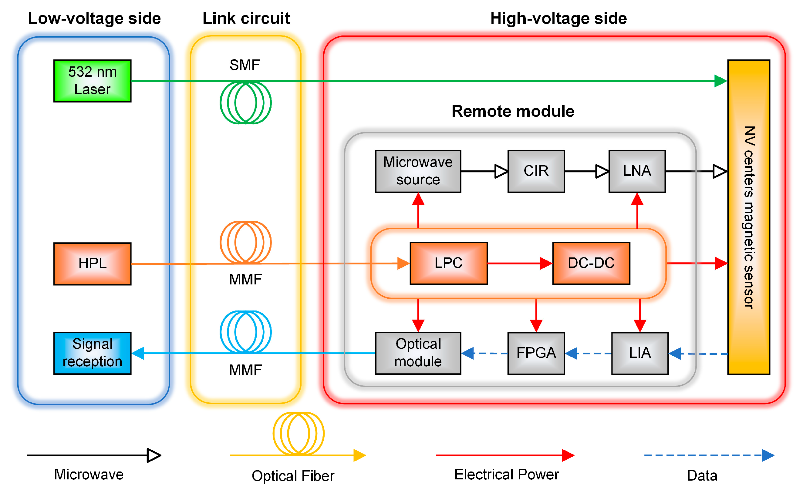
Figure 1. Schematic diagram of UHV NV center magnetic sensing system.
Photonics 12 01093 g001
Figure 2. Designed LPC assembly according to system requirements. (a) Schematic of the 6-junction LPC structure; (b) physical image of the wafer and magnified chip view; (c) simplified model of the optical path (comprising sealing glass, collimating lens, and corner cube retroreflector (CCR)); (d) fabricated high-power assembly with dimensions of 64 mm × 48 mm × 22 mm.
Photonics 12 01093 g002
Figure 3. I-V and P-V characteristics of the prepared assembly under different laser powers with an 830 nm wavelength. The hollow points are the I-V characteristics, and the solid points are the P-V characteristics.
Photonics 12 01093 g003
Figure 4. Output electrical power and efficiency characteristics of the prepared assembly under laser power with 830 nm wavelength from 1 to 10 W. The red line is the efficiency–power trend line of the prepared assembly under different laser powers.
Photonics 12 01093 g004
Figure 5. NV center magnetic sensing system for UHV scenarios. (a) Physically constructed system; (b) NV center sensor with dimensions of 33 mm × 24 mm × 5 mm, hermetically sealed in nitrogen; (c) physical image of the remote module, featuring redundant backup for LPC assembly; (d) simplified schematic diagram of the system.
Photonics 12 01093 g005
Figure 6. Magnetic sensing performance of the system. (a) NV center ODMR test curves: (i) ODMR spectrum; (ii) demodulation curve; (iii) first-order derivative curve; (b) low-frequency noise spectrum of the system; (c) long-term stability test results of magnetic sensitivity.
Photonics 12 01093 g006
Figure 7. Full temperature performance test of LPC assembly. LPC assembly and heat sink are placed in a chamber where the temperature is stabilized at the desired value. The LPC is then irradiated via an optical fiber, and the PIV curves are measured.
Photonics 12 01093 g007
Figure 8. Key sensitivity parameters under different microwave powers and laser drive currents. (a) Full width at half maximum (FWHM). (b) Contrast ratio (CR).
Photonics 12 01093 g008
Figure 9. Three-dimensional distribution of measured sensitivity under different modulation frequencies and frequency offset.
Photonics 12 01093 g009
Table 1. Power consumption of high-voltage-side modules.
ComponentPower Consumption (W)Total Power Consumption (W)
LNA0.63.8
RF microwave0.8
NV center sensor0.08
LIA0.8
FPGA0.8
Low-speed optical module0.72
The data in this table represents the estimated power consumption of a single-channel module. For multi-channel systems, the total power consumption approximately exhibits a linear superposition trend, and additional losses caused by the DC–DC conversion process and the operation of control circuits must be taken into account.
Table 2. Comparison of Key Performance Indicators for Typical NV Center-Based Magnetic Sensing Systems.
ReferencesSensitivity
(nT/Hz1/2)
Power Supply ModeApplication ScenarioAdvantagesDrawbacks
Peng X, Xie F, Zhu Y, et al. [28]2.25Electrically driven (with PCB-embedded copper block for heat dissipation)
Total power consumption not specified, laser power of 100 mW
Handheld magnetic detection devices, industrial magnetic field monitoring, biomagnetic imaging (e.g., animal magnetocardiography), magnetically silent environment detectionVolume of only 2.72 cm3
Three-axis vector detection
No obvious thermal drift
Near-surface NV center coherence to be optimized
Relies on local power supply
Laser noise requires a balance between detection efficiency and noise suppression
Our Work6.1Power over Fiber (PoF), 4 LPC modules connected in parallel Total power consumption of the high-voltage side is approximately 15.2 WUHV current/magnetic field monitoring, strong electromagnetic interference environments (e.g., substations, converter stations)All-fiber isolation design
Adaptability to complex working conditions
High precision under strong interference
Relatively high system power consumption
Sensor thermal stability to be improved
Pogorzelski J, Horsthemke L, Homrighausen J, et al. [29]28.32Powered by 9 V battery, constant current source driving LED (30 mA)
Total power consumption of approximately 0.1 W
Automotive current detection, switchgear magnetic field monitoring, temperature-magnetic field combined measurement, portable industrial on-site detectionSignificant cost advantage, with cost ~90% lower than CVD diamonds
Volume of only 0.42 cm3
Ultra-low power consumption
System performance dominated by LED noise
Sensitivity limited by hardware
Dynamic magnetic field detection deviation
Stürner F M, Brenneis A, Kassel J, et al. [30]31Powered by external wired power supply; total power consumption of 1.5 W (including LED and signal amplification circuit)Industrial-grade vector magnetic measurement, equipment magnetic field calibration, low-cost quantum sensing prototype verificationFirst realization of an NV magnetometer integration without external optical equipment
Vector detection capability
Prominent heat dissipation issue
Obvious sensitivity bottleneck
No active thermal control
Ibrahim M I, Foy C, Englund D R, et al. [31]245Electrically driven by CMOS circuit
Total power consumption of 40 mW
Chip-level quantum sensing, integrated NMR spectroscopy, gradient magnetometers, atomic gyroscopesStrong mass production compatibility
Excellent green light suppression
High microwave uniformity
Low NV center density
Dependence on external microwave source
Differential detection noise
Wang X, Zheng D, Wang X, et al. [32]20.77Laser diode driven by self-developed APC circuit (10 mW)
Total power consumption < 200 mW
Portable magnetic detection (e.g., near-surface biomagnetism), industrial equipment magnetic field inspection, field magnetic field measurementAdopts a small laser diode with volume < 10 cm3;
Lightweight probe: Overall weight < 50 g,
Narrow bandwidth
Low system integration
Poor environmental adaptability
Disclaimer/Publisher’s Note: The statements, opinions and data contained in all publications are solely those of the individual author(s) and contributor(s) and not of MDPI and/or the editor(s). MDPI and/or the editor(s) disclaim responsibility for any injury to people or property resulting from any ideas, methods, instructions or products referred to in the content.