1. Introduction
Surface Plasmon Polaritons (SPPs) refer to electromagnetic surface waves arising from the coupling of incident optical fields with free electrons at the metal–dielectric interface [
1]. A key feature of SPPs is their confined electromagnetic field [
2,
3], which reaches maximum intensity at the metal surface and decays exponentially perpendicular to the interface [
4,
5,
6]. These waves can be excited via either electron bombardment or optical excitation [
7]. When metallic structures are fabricated with precise nanoscale dimensions, SPPs can circumvent the diffraction limit of conventional optics [
8,
9], allowing for subwavelength optical confinement and nanoscale light manipulation [
10]. Applications of SPP-based technologies span from single-molecule biosensing and on-chip optical interconnects to highly efficient solar energy harvesting and subdiffraction-limited imaging [
11]. Furthermore, SPPs hold significant promise for emerging fields such as quantum photonics and flexible electronics, indicating a broad potential for future innovations [
12,
13].
Over the past few years, sensors that measure refractive index and are built on MIM waveguides have garnered significant research interest due to their compelling advantages for both scientific and practical applications [
14,
15]. These sensors exhibit strong lateral optical field confinement, relative ease of fabrication, low propagation loss, and compact transmission path lengths [
16]. Furthermore, MIM waveguide configurations can support a range of nonlinear optical effects, including notable phenomena such as electromagnetically induced transparency (EIT) and Fano resonance [
17,
18,
19]. Fano resonance is a distinct form of scattering resonance characterized by a pronounced asymmetric peak in the transmission response. This profile arises from the interference between a confined narrowband mode and an extended broadband mode. The resonance is marked by sharp variations in amplitude and phase, resulting in an extremely narrow FWHM [
20]. Owing to these spectral characteristics—narrow linewidth and enhanced electromagnetic field confinement—Fano resonance offers superior instrumental resolution, making it highly ideal for precise detection and characterization applications [
21].
In this study, we present a refractive index sensor that relies on SPPs [
22,
23], comprising a URRCTR coupled to a MIM waveguide with an inverted rectangular stub. Compared to other cavity configurations, the U-shaped resonator demonstrates heightened sensitivity to minor geometric variations [
24]. The integration of a ring structure atop the U-shaped cavity effectively concentrates the magnetic field, while the two angled rectangular elements significantly enhance sensitivity without compromising bandwidth. Additionally, the vertical elongation of the U-shaped cavity reduces fabrication complexity and suppresses propagation losses. The inverted rectangular stub integrated into the MIM waveguide provides a localized enhancement of the magnetic field, thereby strengthening light–matter interaction across the structure. The transmission properties and normalized electromagnetic field distributions were numerically investigated using the FEM. The asymmetric Fano resonance line shape observed in the transmission spectrum was thoroughly examined, and its physical origin and influencing factors were elucidated [
25,
26]. We further analyzed the impact of various structural parameters and environmental refractive indices on the sensing performance. The optimized sensor achieves a maximum sensitivity of 3480 nm/RIU and a figure of merit (FOM) of 55.23. Owing to its high sensitivity, the device also exhibits a temperature detection capability of 1.75 nm/°C, demonstrating its potential for highly sensitive photonic sensing applications.
2. Materials and Methods
When the wavelength of the incident light is significantly larger than the thickness of the structure, employing a two-dimensional model can effectively minimize computational errors in structural simulations while substantially reducing the computational workload. Leveraging this advantage, a two-dimensional modeling approach was adopted for the simulations in this study.
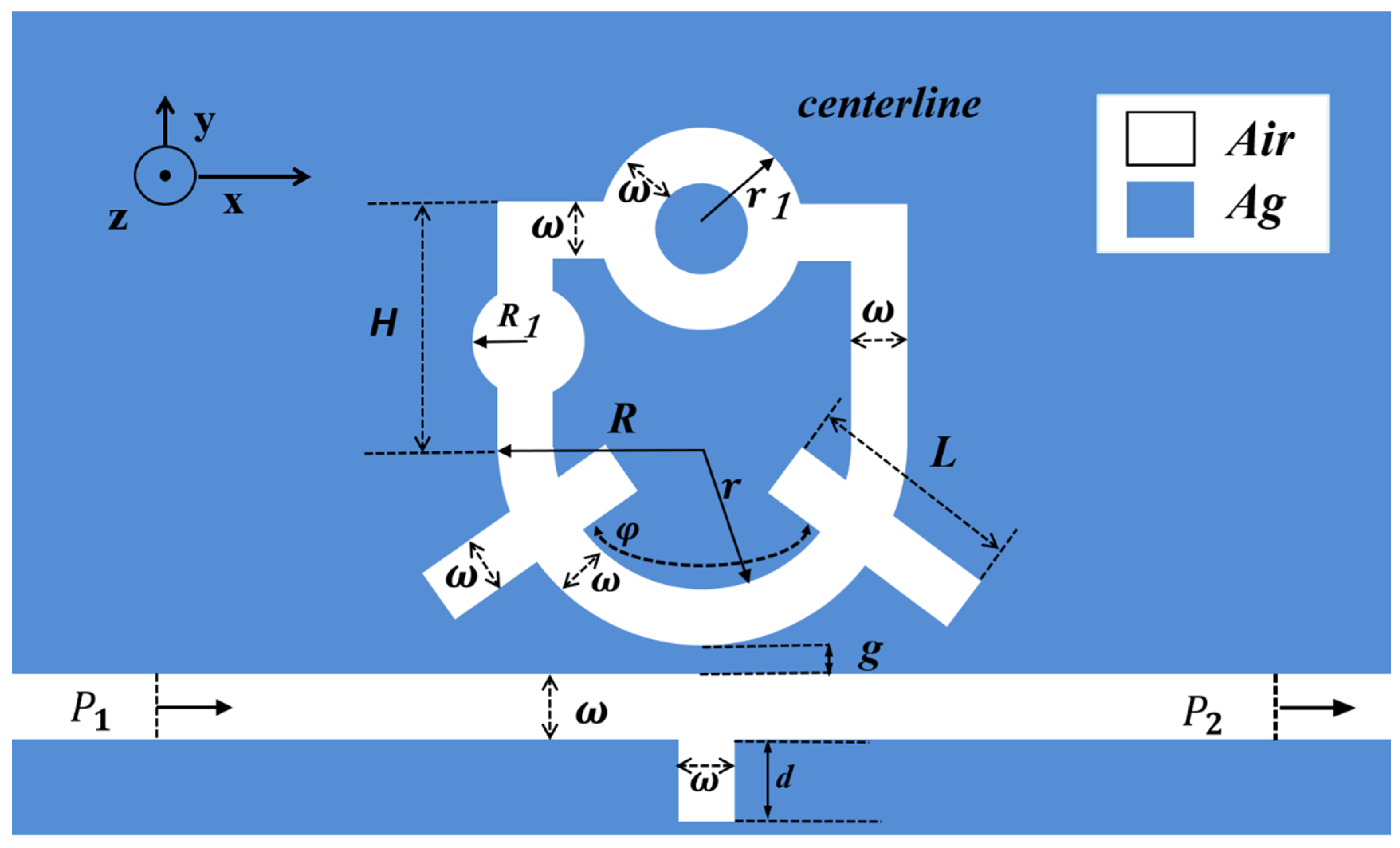
Figure 1 demonstrates the two-dimensional planar schematic of the proposed waveguide-coupled resonator system, which integrates a URRCTR resonator with a MIM waveguide incorporating an inverted rectangular stub. The U-shaped cavity was selected owing to its combined benefits of circular and rectangular resonators.
The dimensional parameters of the design are specified as follows: R denotes the outer radius of the larger ring, r represents its inner radius, R
1 indicates the radius of the circle, and r
1 refers to the outer radius of the upper ring. H is the height of the U-shaped cavity, L represents the length of the two rectangular cavities, d stands for the height of the inverted rectangular stub, and φ indicates the rotation angle of the two rectangular elements. The definitions of the simulation geometric parameters are summarized in
Table 1. The distance of interaction between the inverted rectangular stub waveguide and the URRCTR configuration is represented by g. The widths of the MIM waveguide, rectangular cavities, and ring resonator are uniformly defined as ω. In the diagram, the blue areas represent silver metal, while the white regions correspond to air. Silver was chosen as the metallic material due to its favorable properties, including high stability, strong corrosion resistance, and low optical loss. The dielectric constant of silver is modeled using the Drude dispersion approach, specifically as follows [
27,
28]:
As shown in Equation (1): is the infinite frequency relative permittivity, s, the permittivity of the silver is S/m, is the permittivity in vacuum, is the static dielectric constant.
For the simulations conducted in this study, the electrical properties of silver were represented by the Drude model. Compared to the Lorentz–Drude model, the Drude model provides a more concise description of electronic polarization and is particularly suitable for characterizing the optical response of free electrons in metals [
29]. At the nanoscale, where system size and complexity often constrain the use of more elaborate models, the Drude model offers a favorable balance between simplicity and accuracy. For sensors based on MIM waveguides, key characteristics such as the localized electromagnetic field profile and refractive index changes can be reasonably described using the Drude model. Although the Lorentz–Drude model exhibits broader spectral validity, the Drude model remains sufficient for accurately representing the system response within specific frequency bands of interest. When the coupling distance between metallic interfaces is large, surface plasmon polaritons (SPPs) cannot couple effectively across the two metal–dielectric interfaces [
30,
31]. In contrast, at small coupling distances, SPPs interact to form symmetric modes, specifically the TM
0 and TM
1 modes [
32]. The TM
0 mode is a pure surface wave with no cutoff width, while the TM
1 mode, which has a finite cutoff width, arises from antisymmetric superposition and comprises both surface and oscillatory wave components. To ensure exclusive propagation of the TM
0 mode—an even-symmetric SPP mode—within the MIM waveguide, the dielectric core thickness was set to 50 nm. Accordingly, the waveguide width parameter ω was consistently maintained at 50 nm throughout this study. The TM
0 pattern of the MIM wave guide is evaluated as follows [
33,
34]:
As shown in Equation (2): k is a measure of the waveguide’s loss. , , and represent the relative permittivity of the dielectric and the metal, respectively. The is the free-space wavenumber.
Given the high fabrication costs associated with nanoscale devices, numerical simulation has become an effective alternative, allowing flexible design and optimization of sensor structures to maximize performance. In this study, a two-dimensional model of the overall structure was developed and simulated using COMSOL Multiphysics 5.4. The ports on the left and right sides of the metal–insulator–metal waveguide were set as the input and output ports, respectively, with both port types defined as numerical ports. The light source was incident from the input port with an incident power set to 1 W, while the excitation of the output port was disabled. All boundaries other than the input and output ports were set as a Perfectly Matched Layer (PML) to absorb spillover waves. The wavelength gradually varies from 2100 nm to 3100 nm, with 1 nm as the minimum unit. To ensure computational accuracy, the inverted rectangular stub and the composite resonator consisting of a ring, a circle, and two rectangular elements were discretized with a fine free triangular mesh. The remaining domains were also appropriately meshed to maintain numerical consistency and precision. The effectiveness of the proposed design in this paper can be assessed using two parameters: sensitivity (S) and figure of merit (FOM), which are expressed as follows [
35,
36]:
Here, Δλ and Δn represent the variations in the resonant wavelength and refractive index, respectively. The FWHM denotes the full width at half maximum, which refers to the breadth of the spectral peak at half of its maximum amplitude. Following the preliminary simulations, the wavelength range is chosen to be 2100–3100 nm in a 1 nm step. The initial parameters of the gear structure are given in the following table (
Table 2).
3. Simulation Results and Analysis
Initially, the U-shaped cavity was evaluated independently to assess its intrinsic performance [
37]. Although the standalone U-shaped cavity already demonstrated considerable sensitivity, the incorporation of a ring, a circle, and two rectangular elements further improved its responsiveness. This integrated configuration not only broadened the detectable range of refractive index variation but also increased the FOM. The subsequent introduction of an inverted rectangular stub reduced the FWHM, leading to optimized overall system performance. The parameter values for the final structure were determined as follows: R = 230 nm, R1 = 60 nm, r1 = 100 nm, L = 260 nm, g = 10 nm, d = 90 nm, H = 250 nm,
= 50 nm,
= 35°.
First, we discuss why the asymmetric nanoscale refractive index sensor was selected.
As illustrated in
Figure 2, the red curve corresponds to the symmetric structure formed by coupling the continuous mode of the MIM waveguide with the discrete mode of the U-shaped resonator. Its transmission spectrum exhibits a single broad resonance peak with a FWHM of approximately 100 nm and very high transmittance. In contrast, the black curve represents the asymmetric U-shaped resonator structure, which displays a doublet peak profile in the emission spectrum. This line shape originates from the coupling between two adjacent discrete states and the broadband continuum. The asymmetric resonator yields a more sharply defined resonance, accompanied by a larger resonance wavelength shift, higher sensitivity, and an excellent FOM. For the transmission spectrum with bimodal characteristics, the full width at half maximum (FWHM) was determined by treating the lower-intensity peak as an isolated single peak. The calculation was performed by taking the wavelength difference between the left and right points at half-maximum of the respective peak.
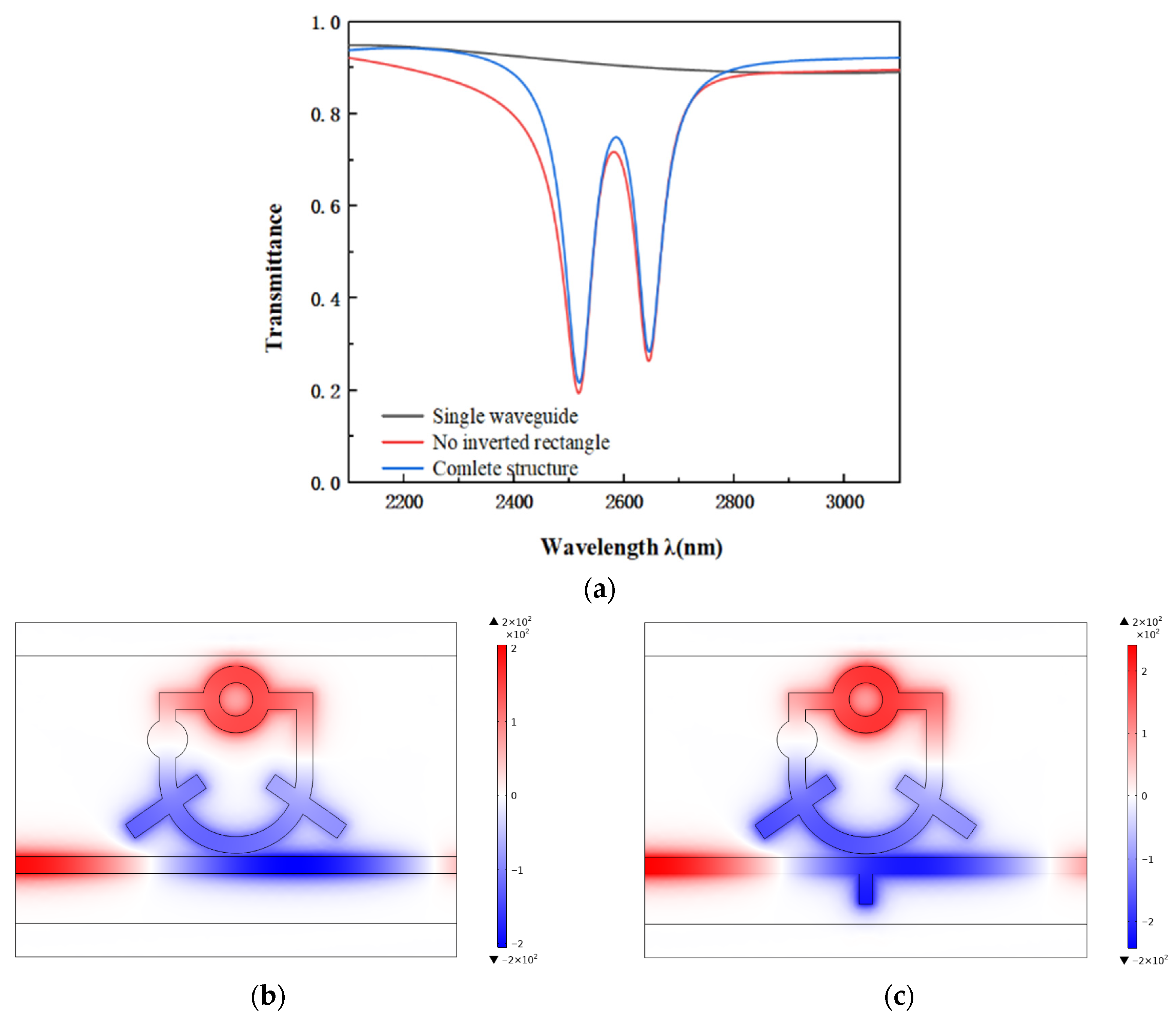
To further elucidate the origin of the Fano resonance, we comparatively analyzed the transmission spectra of three configurations: the single waveguide, the system without the inverted rectangular stub, and the complete integrated structure. Their respective transmission spectra are presented in
Figure 3a. The black curve corresponds to the single waveguide, representing a continuum state characterized by a broad spectral profile resulting from direct excitation of the MIM waveguide under incident light. The red curve depicts the system without the stub, which exhibits a discrete state with high transmittance values between 0.7 and 0.9. In contrast, the blue curve, representing the full system, displays a distinctly smoothed spectral line shape. The characteristic curve results from the interplay between the broadband continuous spectrum of the MIM waveguide and the narrowband discrete mode supported by the U-shaped resonator integrated with the URRCTR. It is evident that although the stub-free structure exhibits a deeper transmission dip than the complete system, its resonance peak is significantly broader. This increased linewidth, attributed to the discrete-state dominance, leads to a significant decrease in the FOM.
Figure 3b,c further present the regularized magnetic field distributions at the resonance dip for two configurations: the straight waveguide coupled with a U-shaped resonator (comprising a ring, a circle, and two rectangular elements) and the complete system incorporating the inverted rectangular stub. At the Ag dielectric boundary, a surface plasmon-polariton propagates. The electromagnetic field is localized near the boundary. This effect is especially pronounced in the visible range. In the infrared, the velocity of the wave tends to the speed of the wave in the dielectric, the localization is small. Evidently, the introduction of the stub significantly modifies the transmission properties of the MIM waveguide. Surface plasmon polaritons propagating along the waveguide generate a localized magnetic field enhancement near the stub region, concentrating magnetic energy and enabling higher mesh resolution and improved computational accuracy in simulations. This intensified field confinement enhances the Fano resonance effect. The presence of the stub also promotes stronger coupling between the magnetic hotspot and the U-shaped resonator, contributing to superior sensor performance. Moreover, the magnetic field distribution exhibits mirror symmetry between the upper and lower sections of the U-shaped resonator. While the overall field pattern resembles that of an isolated U-shaped resonator, the addition of the stub facilitates more efficient propagation of surface plasmon waves throughout the structure, thereby further supporting the formation of the Fano resonance.
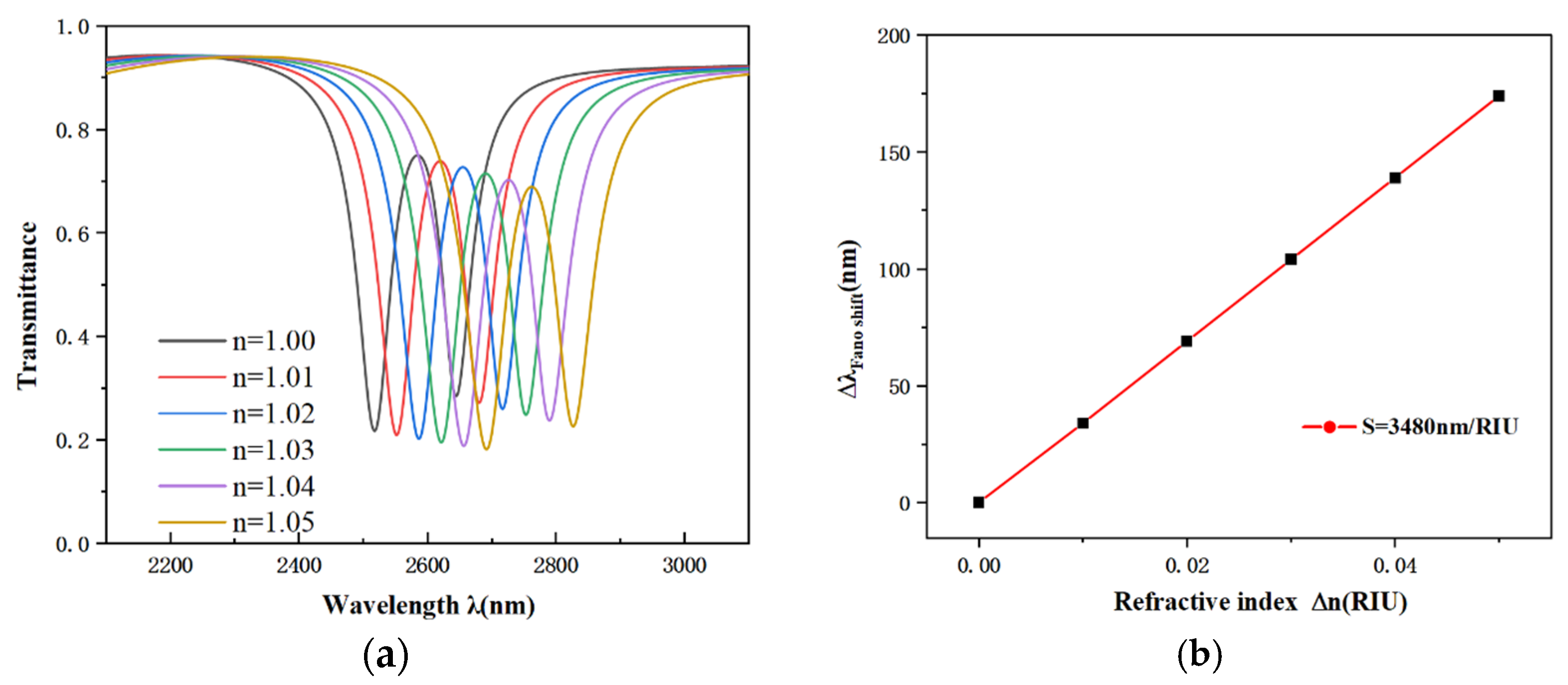
In order to investigate the effect of different refractive indices on the structural performance, a series of discrete values, namely 1.00, 1.01, 1.02, 1.03, 1.04, and 1.05, were selected as control parameters. A comprehensive comparative study was conducted on the results under all these refractive index conditions. As observed in
Figure 4a, as the refractive index n increases, the overall shape of the transmission spectrum remains consistent, while the peak position exhibits an approximately equidistant red shift without significant alteration in the spectral profile.
Figure 4b demonstrates that the observed wavelength shift follows a strong linear relationship with the change in refractive index (n).
The high sensitivity and excellent linearity demonstrated by this structure provide a solid foundation for its application in our proposed sensor. Under the optimal set of parameters, the finalized sensor achieves outstanding performance, with a high sensitivity of 3480 nm/RIU and a FOM of 55.23.
The five different radius values, denoted as
, are shown in
Figure 5a. When a 10 nm step size is used for Fano resonance, the transmission curve exhibits significant variations, with the relative heights of the two peaks differing. As r
1 increases from 80 nm to 120 nm, the entire spectrum shifts toward longer wavelengths, indicating an increase in the wavelength sensitivity (S) and thus enhanced sensor sensitivity. When r
1 is 80 nm, 90 nm, or 100 nm, the left peak exhibits the minimum wavelength. For other values, the right peak shows the minimum wavelength, along with a gradual increase in transmittance. As illustrated by the sensitivity fitting curve in
Figure 5b, the wavelength response of the structure demonstrates a highly linear dependence with changes in the light refractive coefficient.
Figure 5c reveals that the FWHM reaches its minimum at r
1 = 100 nm, following a trend of initial decrease followed by an increase. Combined with the results from
Figure 5b, although the sensitivity continues to improve with larger r
1, the FWHM also broadens. Based on performance evaluation, the configuration with r
1 = 100 nm offers a broad operational wavelength range, and its combination of sensitivity and FOM best meets the requirements for this refractive index sensor. All ring radius configurations support the same fundamental resonance mode, yet differences in their response characteristics can be attributed to the spatial arrangement of the ring cavity, which serves as the core region for energy localization. Therefore, the following discussions are based on the case where r
1 = 100 nm.
The lengths of the two rectangular cavities, denoted as L, were varied from 240 nm to 280 nm in increments of 10 nm, to further investigate the U-shaped resonator with the URRCTR structure.
Figure 6a reveals a positive correlation between the resonant wavelength and the parameter L: an increase in L induces a notable red shift, indicating that active tuning of the spectral response can be achieved by adjusting L. This behavior is attributed to the increased effective refractive index of the optical resonator resulting from larger values of L, which modifies the resonant condition and leads to a displacement of the resonance wavelength, though it has limited effect on modulating the resonance depth. As illustrated in
Figure 6b, the system sensitivity remains stable across the evaluated range of L, demonstrating insensitivity to changes in the rectangular cavity length.
Figure 6c indicates that the FWHM first decreases and then increases with increasing L, reaching a minimum value of 63 nm at L = 260 nm. As L increases from 260 nm to 280 nm, the FWHM broadens significantly from 63 nm to 73 nm.
Given that the length L is a decisive parameter for controlling the transmission spectrum and sensitivity, the results confirm that L = 260 nm achieves optimal frequency precision and overall sensing performance. Based on a systematic evaluation of the spectral response and sensitivity, 260 nm is identified as the optimal length for the two rectangular cavities, offering the best trade-off among all performance metrics.
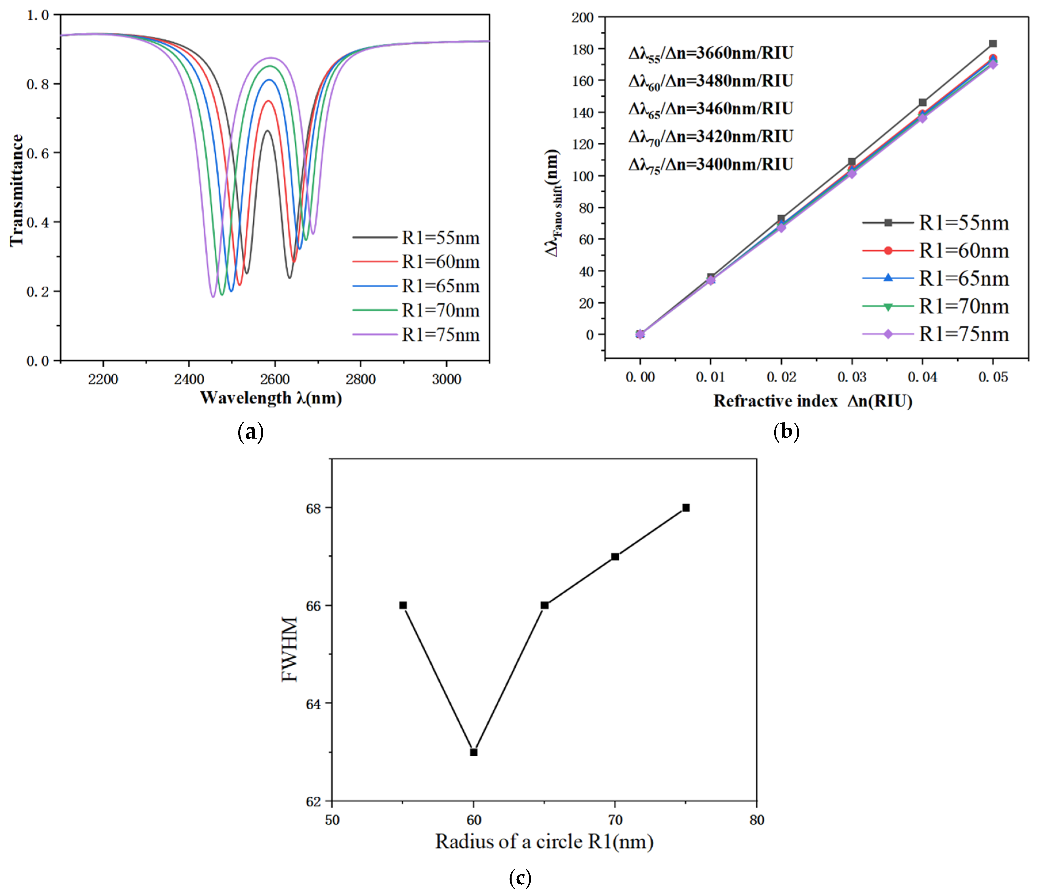
Building upon this foundation, we conducted an in-depth analysis of the critical influence of parameter R
1 on system performance. By setting R
1 to a series of discrete values (55–75 nm), we successfully induced a significant spectral red-shift effect, accompanied by a gradual increase in wavelength. This confirms that R
1 is an effective parameter for tuning the resonant wavelength (
Figure 7a). As illustrated by the sensitivity fitting curve in
Figure 7b, the wavelength response of the structure exhibits a highly linear relationship with changes in the refractive index.
Figure 7c demonstrates that the FWHM attains its lowest value when R
1 = 60 nm. In conjunction with the findings presented in
Figure 7b, although the highest sensitivity occurs at 55 nm, the FWHM also increases accordingly. As R
1 increases from 60 nm to 75 nm, the sensitivity gradually decreases while the FWHM continues to broaden. It is also noteworthy that as the radius increases, the sensitivity declines from 3660 nm/RIU to 3400 nm/RIU, indicating that R
1 is a critical parameter influencing both the S and the system’s FOM. Taking all results from
Figure 7 into consideration, the system achieves optimal performance when R
1 is set to 60 nm.
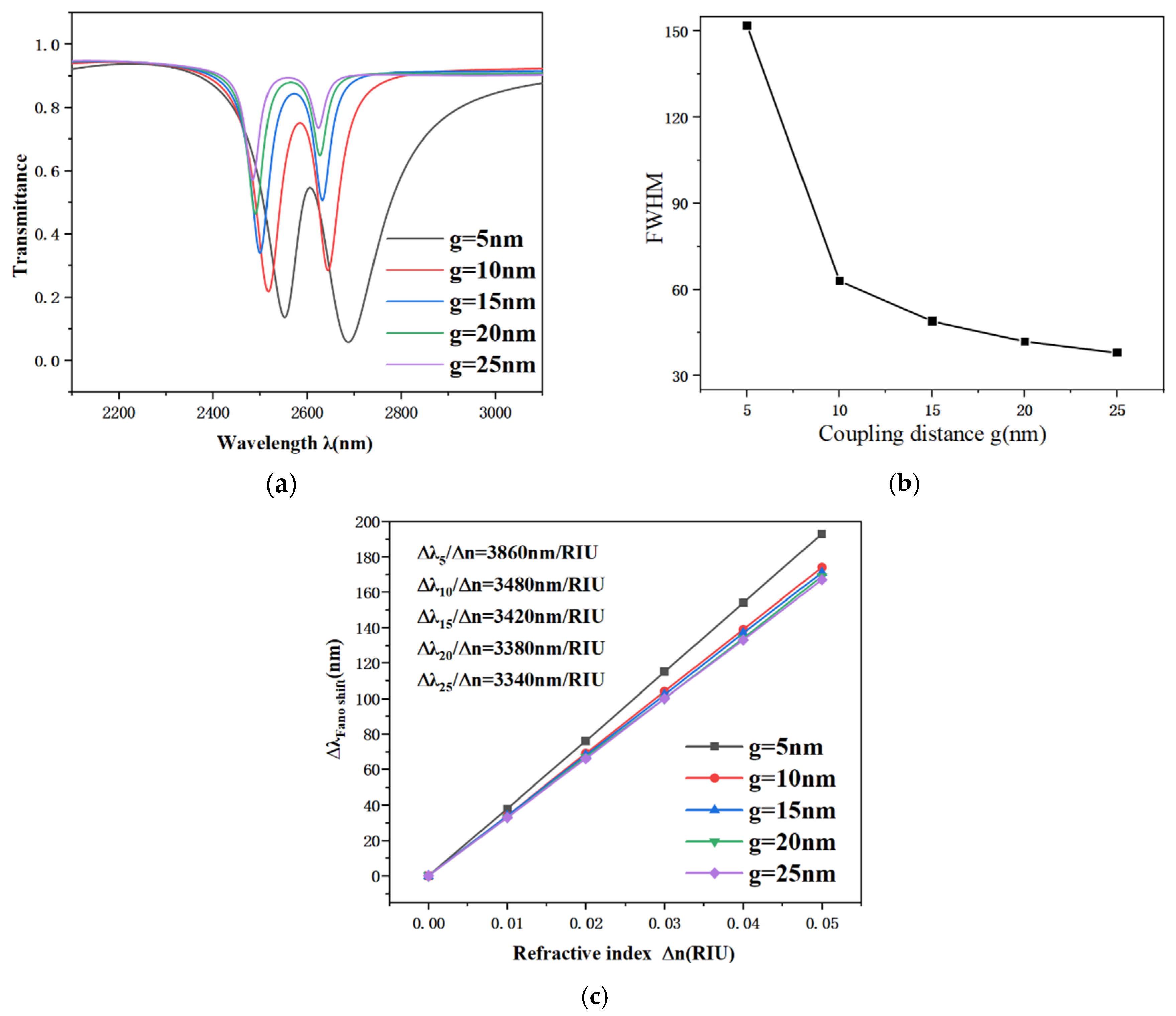
Lastly, the impact of the coupling gap g between the resonator and the waveguide on the sensing performance was comprehensively analyzed.
Figure 8 shows the transmission spectra obtained under different values of g. While keeping the remaining design parameters constant, the coupling gap g was incrementally increased from 5 nm to 25 nm to analyze its effect on the spectral response and sensing characteristics. Analysis of
Figure 8a indicates that as the coupling gap g increases, the transmission characteristics exhibit a notable blue shift, accompanied by an increase in transmission. The enlargement of the coupling gap reduces the coupling efficiency of surface plasmon waves, allowing more energy to be transmitted directly through the waveguide outlet and significantly weakening the electric field within the resonator. As shown in
Figure 8b, this change is directly reflected in a reduction in the FWHM of the transmission profile, along with a corresponding decrease in electric field intensity within the resonant region. Therefore, the selection of the coupling distance g is critically important. As observed in
Figure 8b, when g increases from 5 nm to 10 nm, the FWHM of the transmission spectrum decreases sharply. For coupling gaps larger than 10 nm, the rate of decrease in FWHM slows down. Although a sensitivity of 3860 nm/RIU was achieved at g = 5 nm, it resulted in a broad FWHM of 152 nm, limiting the figure of merit (FOM) to a relatively low value of 25.39. Thus, the coupling performance of the structure was compromised by the large FWHM.
Figure 8c shows that as the coupling gap widens, the sensitivity decreases from 3860 nm/RIU to 3340 nm/RIU. Based on comprehensive evaluation, the optimal coupling gap is determined to be 10 nm. At this point, the designed refractive index sensor reaches a S of 3480 nm/RIU and a FOM of 55.23, which is better than the data in
Table 3.
4. Application
The sensor proposed in this study not only possesses a simple structure but also achieves exceptionally high sensitivity, rendering it highly suitable for temperature sensing applications. Its design aligns well with the practical demands for device miniaturization and high integration. To meet the performance requirements of the U-shaped resonator integrated with a circular ring and two rectangular elements, ethanol was selected as the filling material owing to its large thermo-optic coefficient (3.94 × 10
−4 °C
−1) [
39,
40], which ensures outstanding temperature sensitivity. In contrast, silver and silica exhibit substantially lower thermo-optic coefficients (8.60 × 10
−6 °C
−1 and 9.30 × 10
−6 °C
−1, respectively), resulting in inadequate responsiveness to temperature variations; thus, they were deemed unsuitable as filling media. The use of ethanol significantly enhances the temperature detection performance of the hybrid resonator system. Its high efficiency and reliability originate from the strong linear positive correlation the relationship of the refractive index of ethanol with temperature over an extremely broad range—from its melting point of −144 °C to its boiling point of 78 °C—which constitutes the fundamental mechanism of ethanol as a highly responsive sensing medium. The refractive index of ethanol as a function of temperature can be described by the following formula [
41]:
T represents the ambient temperature, and
denotes room temperature, typically set at 20 °C. To fundamentally ensure measurement reliability, the operational temperature range of the sensor (−80 °C to 70 °C) is strictly confined within the liquid phase of ethanol. This aims to maintain the stability of its refractive index properties and effectively avoid measurement errors caused by material phase transitions. The structural parameters are configured as follows: g = 10 nm, R = 230 nm, R1 = 60 nm, r1 = 100 nm, H = 250 nm, L = 260 nm, d = 90 nm,
= 35°,
= 50 nm. The sensor operates based on the strong thermo-optic effect of the ethanol medium. By precisely monitoring the change in the resonance profile, changes in the refractive index are derived, thereby enabling the retrieval of temperature information. As such, the sensitivity of this temperature sensor can be expressed by the following formula [
38,
42]:
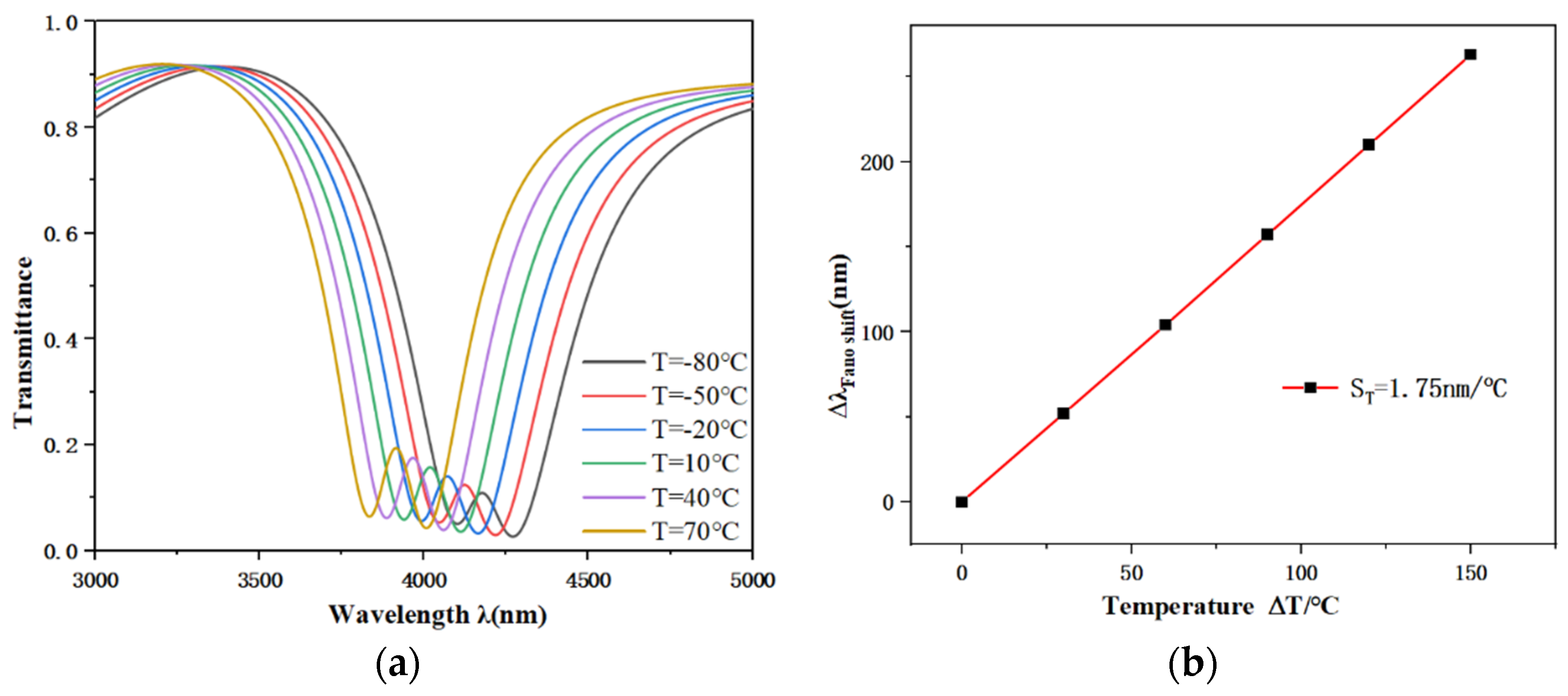
For the specified temperature range, the temperature variation (ΔT) is defined as 150 °C, with Δλ indicating the shift in the transmission profile.
Within this temperature range, as indicated by Equation (5), the variation in the optical index of the designed structure spans from 1.34078 to 1.39988. According to
Figure 9a,b, this change can be quantified by the red shift of the transmission dip from 4007 nm to 4270 nm, resulting in a resultant wavelength shift (Δλ) of 263 nm. The sensor’s sensitivity is determined to be 1.75 nm/°C, a value derived from the linear regression of the curve illustrated in
Figure 9b, thereby ensuring the reliability of the measurement. This high sensitivity serves as a crucial indicator of exceptional temperature measurement performance, offering a dependable solution for various applications requiring precise thermal management. The practical fabrication of such precise gaps presents considerable challenges. While advanced techniques like electron beam lithography and focused ion beam milling are capable of creating sub-10 nm features in localized areas, they face critical hurdles in controlling surface roughness and avoiding material damage. These imperfections can introduce additional damping, thereby degrading the device’s quality factor. Consequently, limitations in nanofabrication currently lead to discrepancies between simulated and actual sensor performance. This gap, however, is expected to narrow with continued advancements in nanomanufacturing capabilities.
