1. Introduction
Light detection and ranging (LiDAR) sensors have been frequently utilized in various applications, such as autonomous vehicles and drones, remote sensing systems, indoor mapping sensors, and home-monitoring sensor systems [
1,
2,
3,
4,
5,
6]. Typically, LiDAR sensors utilize either direct time-of-flight (dToF) or indirect time-of-flight (iToF) measurement schemes, depending on the specific target applications. The former directly estimates the detection range with the time difference between the transmitted pulse and the received pulse, while the latter calculates the target distance indirectly from the phase delay between the emitted and reflected pulses. In particular, the iToF scheme has recently gained popularity for applications in robots, unmanned aerial vehicles, and/or autonomous cars because it is more efficient for detection ranges up to several tens of meters. In addition, it can employ low-cost CMOS camera imaging technologies to generate faster and higher currents and, consequently, finer images. Nonetheless, either the dToF or iToF scheme is primarily dependent upon the receiver architecture; therefore, the transmitter (also known as a laser-diode driver or a VCSEL driver) can be commonly incorporated in either scheme.
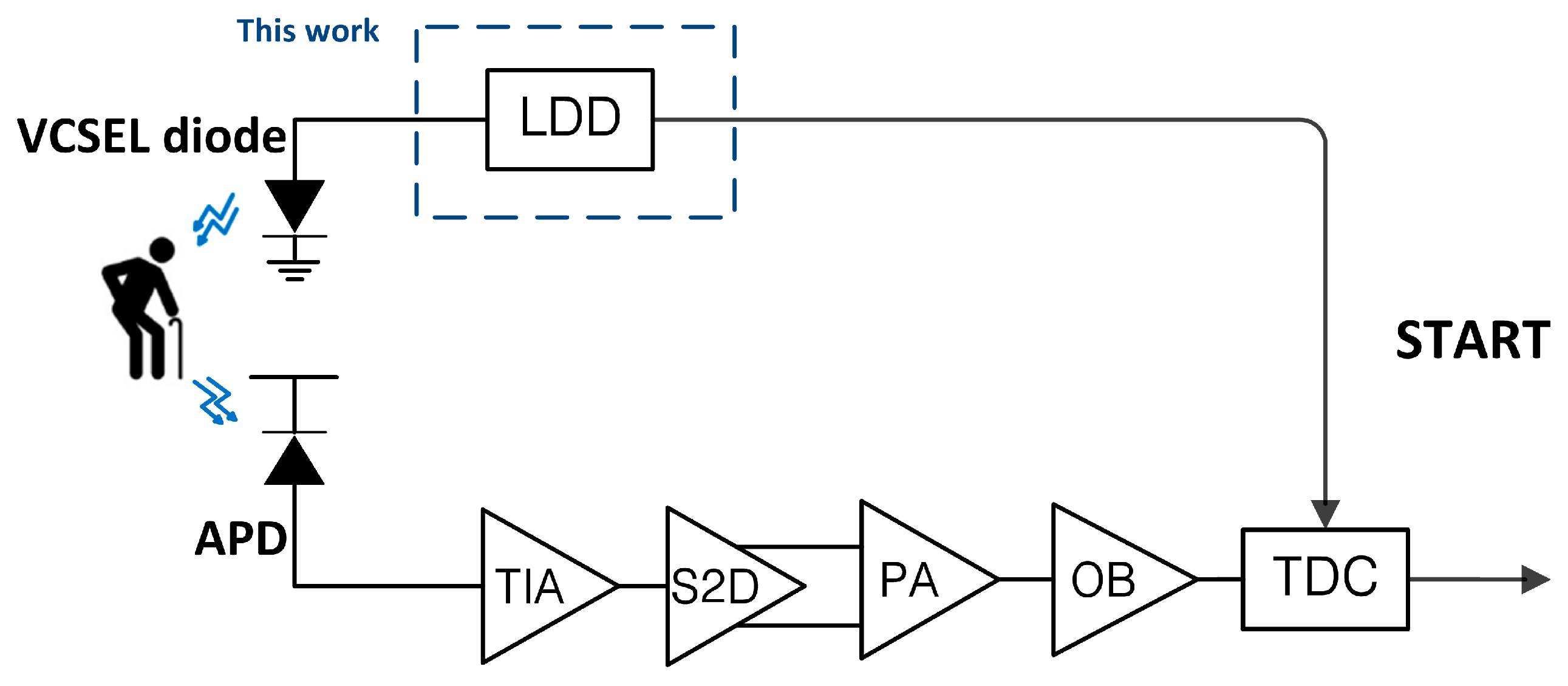
Figure 1 shows the simplified block diagram of a LiDAR sensor, where a laser diode driver (LDD) simultaneously emits optical pulses to targets via a laser diode and a START pulse to the time-to-digital converter (TDC) in the receiver. Then, the transmitted optical signals are reflected and received by the LiDAR receiver, which consists of an avalanche photodiode (APD) to convert optical pulses into electrical current signals, a transimpedance amplifier (TIA) to change the converted current signals to output voltages, a single-to-differential (S2D) converter to acquire differential signals and thus to achieve a better power supply rejection ratio (PSRR) characteristic, a post-amplifier (PA) to boost the output voltages of the preceded TIA, and a TDC to estimate the timing delay between the START pulse and the processed (also known as STOP) pulse in the receiver. In general, laser diodes are costly and require large bias voltages sometimes, whereas vertical-cavity surface-emitting laser (VCSEL) diodes are inexpensive and operate with much lower bias voltages, thus leading to more reliable functions for short-range LiDAR sensors with low-cost and low-power characteristics. Therefore, many researchers have suggested a number of novel optical transmitters realized in sub-micron CMOS technologies for the applications of LiDAR sensors and optical interconnects. Particularly, costly LDDs have been preferably exploited in long-range LiDAR sensors because they can emit narrow and strong pulses. However, for short-range indoor monitoring LiDAR sensors, low-cost and low-power VCSEL drivers would become more attractive, especially for applications aimed at the fall detection of senile Alzheimer patients living either at home or in long-term care facilities [
2].
As aforementioned, VCSEL diodes operate with low supply voltages because they require a forward voltage slightly greater than 1.5 V. Therefore, the supply (V
DD) of the VCSEL drivers can be selected to be 3.3 V to ensure the robust operation of the VCSEL diodes. Yet, there exists an inevitable bond-wire inserted between the VCSEL diode and the VCSEL driver circuit, which gives rise to a serious design issue, i.e., a large voltage headroom in a DC-coupled LDD (or VCSEL driver) [
7,
8,
9].
Typically, two different VCSEL drivers are exploited, i.e., a common-anode VCSEL driver and a common-cathode VCSEL driver. Usually, the former can bias the VCSEL diode with an external voltage (V
DD,VCSEL) higher than the supply (V
DD). Also, this common-anode architecture can decrease the DC power dissipation substantially [
9]. However, since the exploitation of a common-anode VCSEL diode demands an additional V
DD,VCSEL, it would increase the packaging cost and the complexity of testing boards. On the contrary, a common-cathode VCSEL driver can reduce the voltage headroom issue effectively and also provide compatibility with the stringent design requirements and constraints [
10,
11,
12,
13,
14].
This paper is organized as follows:
Section 2 shows conventional voltage-mode VCSEL drivers.
Section 3 describes the proposed modified current-mode VCSEL driver.
Section 4 shows the post-layout simulation results. Then, the conclusion is presented.
2. Previous Voltage-Mode VCSEL Drivers
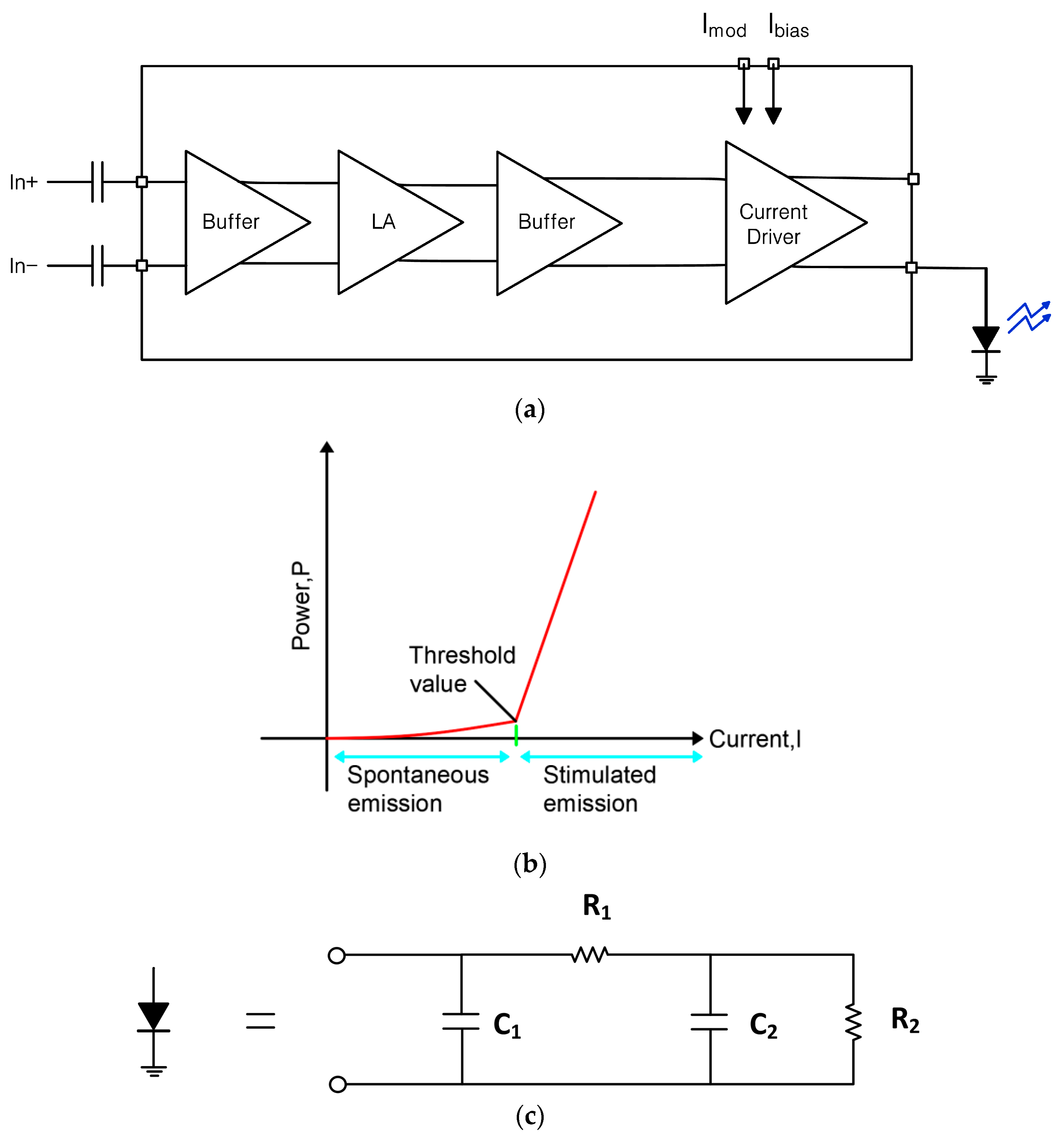
Figure 2a depicts the architecture of a voltage-mode VCSEL driver, which comprises a buffer input for self-biasing and 50 Ω impedance matching, a limiting-amplifier (LA) stage to boost the input signals, an additional buffer to isolate the LA from the following main driver in terms of the parasitic capacitance and the DC offset voltages, and a main driver to generate the final output currents for the VCSEL diode. In particular, the differential signals are AC-coupled through external capacitors at the input.
Figure 2b illustrates the characteristic curve of the current (
I) flowing through the VCSEL diode and the corresponding output power (
P), which shows two modes of the optical power emission, i.e., spontaneous emission and stimulated emission. The former occurs when the bias current of the VCSEL diode is below the threshold value (
Ith), where the emission of the optical power nearly disappears. The latter occurs when the bias current of the VCSEL diode is above the threshold (
Ith). Then, the optical power increases abruptly and almost linearly, hence clearly demonstrating the importance of the operations above the threshold current to achieve an efficiently stimulated emission.
For circuit simulations, the VCSEL diode is transformed into an electrically equivalent model so that its behaviors can be predicted as precisely as possible.
Figure 2c depicts the equivalent circuit of a VCSEL diode with the target wavelength of 850 nm, which includes a resistor (
R1) representing the signal loss, a capacitor (
C1) denoting the capacitance of the optical cavity, a capacitor (
C2) describing the capacitive effect, and a resistor (
R2) as an external load impedance (50 Ω). This equivalent circuit model can be incorporated to analyze the response of a VCSEL diode at wide-range frequencies and to optimize the performance of VCSEL drivers, particularly for short-range LiDAR sensors, thus enhancing the system’s efficiency and stability [
15].
Figure 2.
(
a) Block diagram of a voltage-mode VCSEL driver, (
b) the characteristic curve of a VCSEL diode, and (
c) an equivalent model of a VCSEL diode for circuit simulations [
16,
17].
Figure 2.
(
a) Block diagram of a voltage-mode VCSEL driver, (
b) the characteristic curve of a VCSEL diode, and (
c) an equivalent model of a VCSEL diode for circuit simulations [
16,
17].
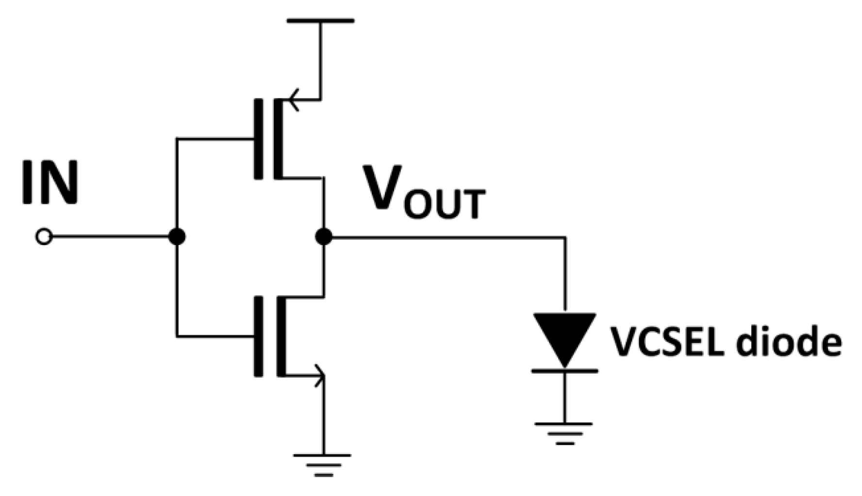
Conventionally, voltage-mode logic (VML) circuits have been exploited as VCSEL drivers. An example is a push-pull inverter architecture of which a schematic diagram is shown in
Figure 3 together with a VCSEL diode. Here, it is clearly seen that currents are flowing through the VCSEL diode via the pull-up transistor (PMOS) and that the amplitudes of currents in this VML driver are only half of those in a current-mode logic (CML) driver. Then, the total power dissipation of a VML driver can be reduced. However, the output impedance of a VML driver is dependent on the parallel combination of the NMOS/PMOS on-resistances. Thus, it can be highly sensitive to variations in the manufacturing process. Furthermore, although a typical VML driver exhibits low power consumption characteristics at low-frequency operations, its efficiency may not be as high as that of a CML driver, especially for high-frequency applications, thereby restricting the output signal swings. This defect may affect the signal quality during the optical emission mode. Hence, we prefer a current-mode VCSEL driver in this work.
3. Modified Current-Mode VCSEL Driver
Figure 4 depicts the simplified block diagram of the proposed modified current-mode VCSEL diode driver (m-CMVD), where the bias current (I
BIAS) control and the modulation current (I
MOD) control are facilely merged, not only to reduce the chip area considerably but also to enable the reliable operations of the VCSEL diode. Previously, a similar topology was presented in [
17], where a tree-like output driver with 100 driver cells was employed to drive a common-anode VCSEL diode. Each cell consisted of an inverter followed by an NMOS cascode circuit with a thick-gate common-gate transistor, consequently driving up to 5 mA
pp. This tree-like architecture mandated a very careful layout to avoid delay mismatches, and the final results demonstrated severe peaking and distortions.
Also, a modified current-steering logic (m-CSL) is incorporated to produce the modulation currents flowing through the VCSEL diode and to vary the magnitudes of the modulation currents more effectively than the VML drivers. Also, the m-CSL replaces PMOS/NMOS transmission gates with simple NMOS switches to drive the VCSEL diode, resulting in considerably decreased distortions of the output pulses. Moreover, the architecture of the m-CMVD is quite simple for circuit designers.
Nonetheless, an inevitable disadvantage exists in this configuration, i.e., a single-ended architecture. Thus, this single-ended m-CMVD circuit might be sensitive to common-mode noises, e.g., power supply noises. However, this defect can be significantly alleviated by employing external voltage regulator chips that are integrated on a testing PC-board.
In the m-CMVD shown below, the bias generator utilizes a wide-swing current mirror circuit to generate the reference current of 1 mA. The modulation currents of 100 µApp~10 mApp are derived through the parallel AND gates with the input voltage (Vin) and six switches (from A to F). Namely, these six input buffers (IBs) are concurrently biased by the DC current from the wide-swing current mirror circuit. They are either turned on or off by the amplitudes of the input signals, thereby flowing the generated modulation currents into the external VCSEL diode.
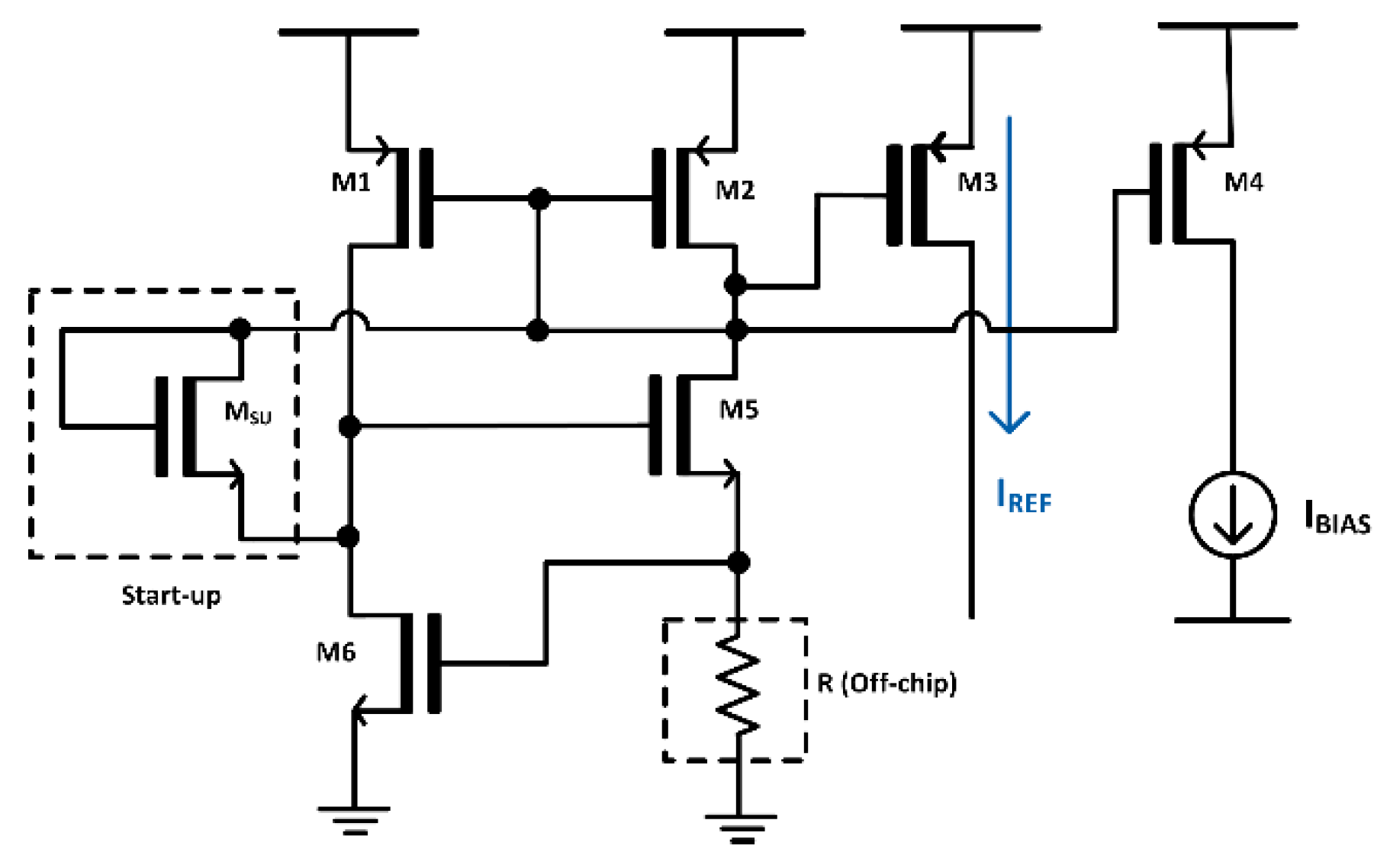
Figure 5 illustrates the schematic diagram of the bias generator in more detail, where the gate-source voltage (V
gs6) of M
6 is carefully designed to be approximately identical to its threshold voltage (V
th), i.e.,
Here, an off-chip precision resistor (R) is utilized so that the effect of temperature can be negligible with less than 1% variation. Then, the generated reference current (Iref) can be almost independent of temperature, voltage, and process (PVT) variations. Hence, the resulting bias current (IBIAS) can be nearly constant.
A diode-connected transistor (M
SU) is added to the gate of M
5, not only as a startup transistor, but also to ensure that M
5 does not enter the cutoff region. Therefore, the gate voltage of M
5 can be equal to V
DD − |V
SG2| − V
gs_su. As long as the supply voltage (V
DD) is sufficiently high, the gate voltage of M
5 cannot be too low, thus preventing the transistor from entering the cutoff region. Hence, this condition can be satisfied with (2)
According to the simulations of PVT variations for the bias generator, the modulation currents deviate a maximum of 15% in the worst case of SS (slow NMOS and PMOS), with a 2.97 V supply voltage at 125 °C. This indicates that the proposed bias generator guarantees stable operations against significant PVT variations.
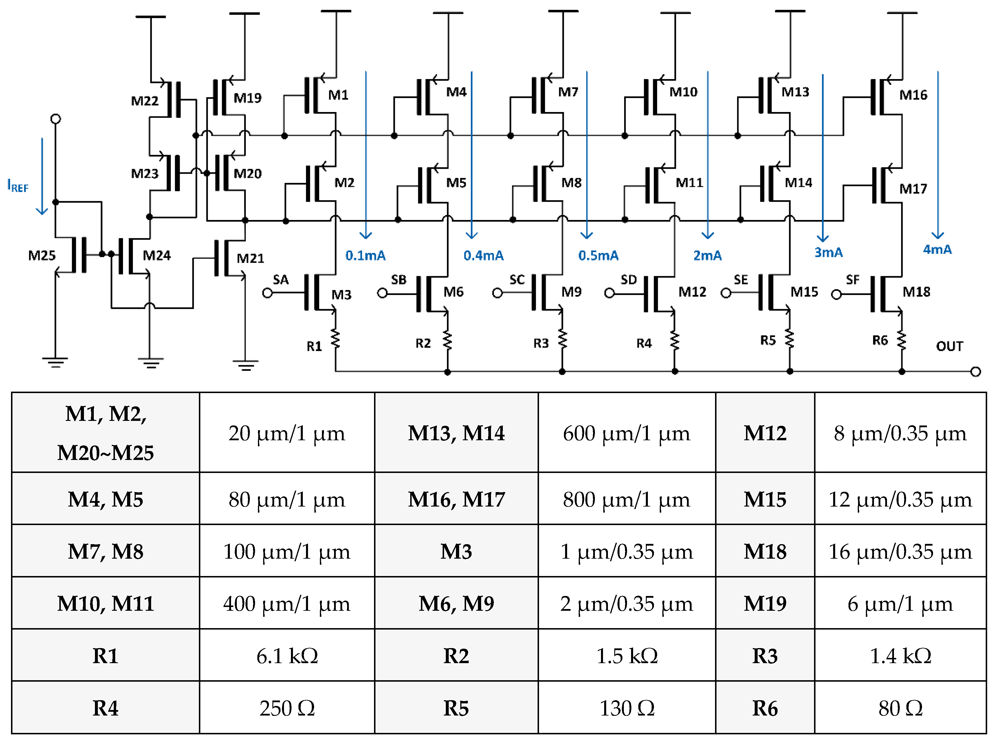
Figure 6 shows the schematic diagram of the m-CSL circuit in detail. Here, a reference current from the bias generator is mirrored into the NMOS current mirror transistors (M
24 and M
21). Then, it is transferred by utilizing the parallel NMOS switches (M
3, M
6, M
9, M
12, M
15, and M
18), which can be turned on or off by the six switches (SA~SF). In our previous work in [
17], the PMOS/NMOS transmission-gates were employed for this switch configuration. However, the severe relaxation oscillations at low modulation currents might be attributed to these transmission-gates because of their large parasitic capacitance. Therefore, NMOS-only switches are exploited in this work, which are more suitable for low-level signals and result in considerably reduced overshoots of the output pulses. Simulations of the m-CSL circuit prove that the troublesome overshoot has nearly disappeared.
Meanwhile, the diode-connected PMOS transistors (M19 and M20) determine the DC voltages of the PMOS current mirror circuits. Thereafter, the total currents of the PMOS current mirror circuits can flow accordingly toward the VCSEL diode, as long as the gate voltages can be lower than the threshold voltage, i.e., VG < VDD − |VTHP|. Here, VTHP represents the threshold voltage of a PMOS transistor.
The simulations of PVT variations for the m-CSL circuit reveal that the modulation currents deviate a maximum of 22.6% in the worst case of FF (fast NMOS and PMOS), with a 2.97 V supply voltage at 125 °C. This indicates that the proposed m-CSL block confirms stable functions against significant PVT variations.
4. Layout and Simulation Results
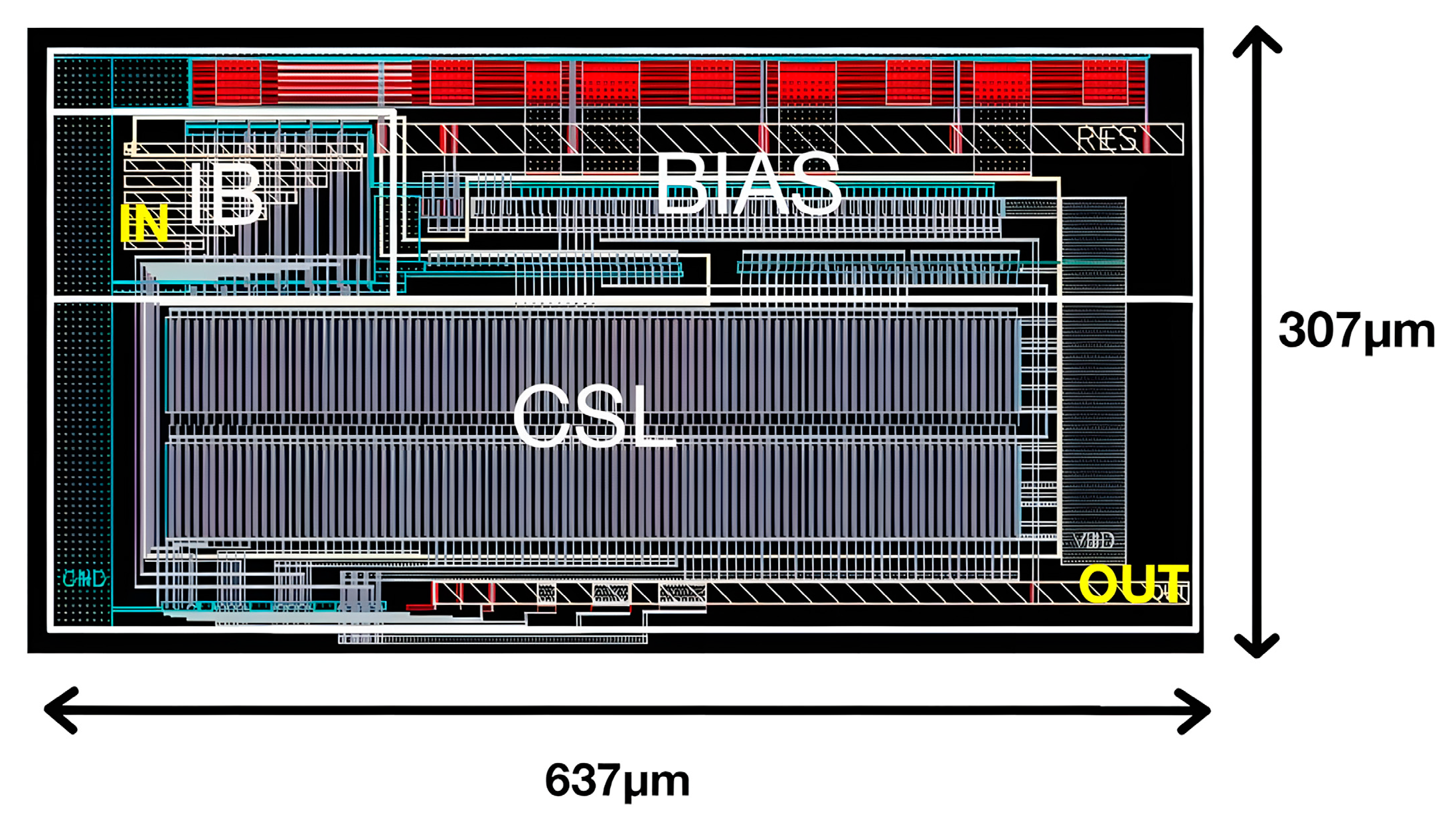
Figure 7 depicts the layout of the proposed m-CMVD circuit, where the fabricated chip occupies a core area of 0.196 mm
2. Post-layout simulations were conducted using a standard 180 nm CMOS process. DC simulations reveal a maximum power consumption of 11 mW from a single 3.3 V supply.
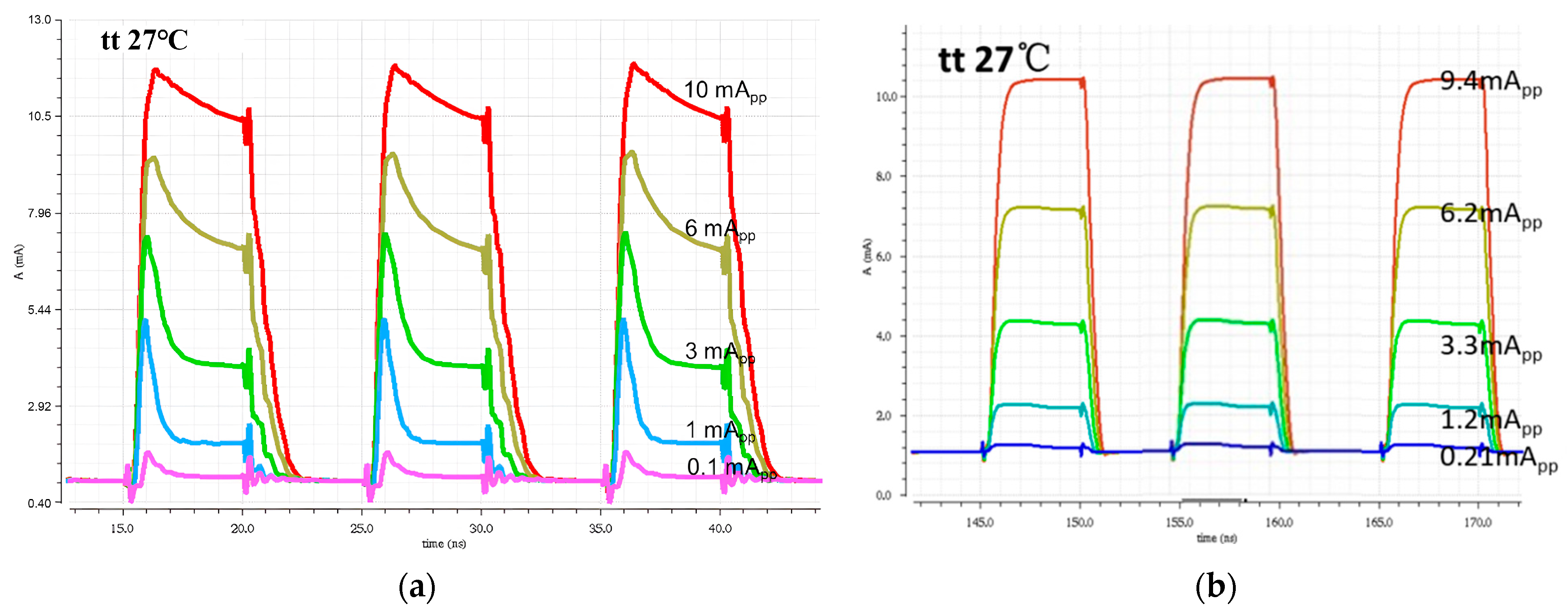
Figure 8 compares the simulated pulse responses of the m-CMVD circuit with those of the previous CMVD reported in [
17], under the same conditions, with a pulse width of 5 ns and modulation currents ranging from 0.1 mA
pp to 10 mA
pp. It is clearly observed that the troublesome overshoots are almost discarded in the proposed m-CMVD circuit.
Figure 9 shows the simulated pulse response of the m-CMVD circuit for the input pulses with two different pulse-widths. It is clearly seen that the previous m-CMVD suffers no overshoot distortions, even with narrower 3 ns pulses.
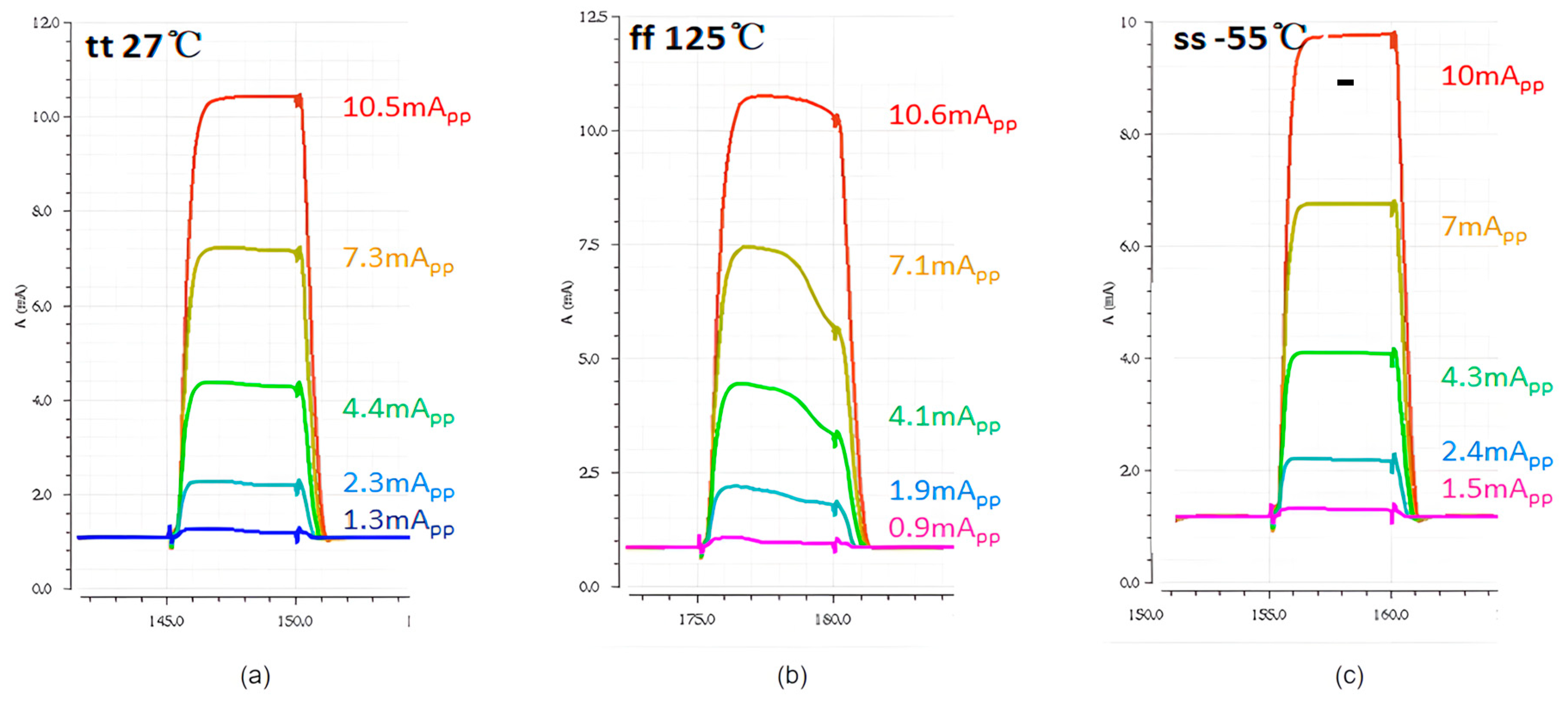
Figure 10 depicts the simulation results of PVT variations for the proposed m-CMVD circuit in three worst-case corners, where the
x-axis indicates the time (in ns) during the transient simulations and the
y-axis shows the combined currents (=I
BIAS + I
MOD) flowing through the VCSEL diode at different temperatures, from −55 °C to 125 °C.
As shown in
Figure 10a, with the wide range of modulation currents (0.1~10 mA
pp), the combined output currents for the case of TT corners are slightly different from the theoretical values (1.1~11 mA
pp), i.e., 4.5% for 11 mA
pp and 15.4% for 1.1 mA
pp. For the case of FF corners (as shown in
Figure 10b), the combined currents deviate from the nominal values of the TT case, 30.8% for the minimum current and 0.95% for the maximum current. Finally, for the case of SS corners (as shown in
Figure 10c), the combined currents differ from the nominal values of the TT (typical NMOS and PMOS) case, 15.4% for the minimum current and 30.8% for the maximum current.
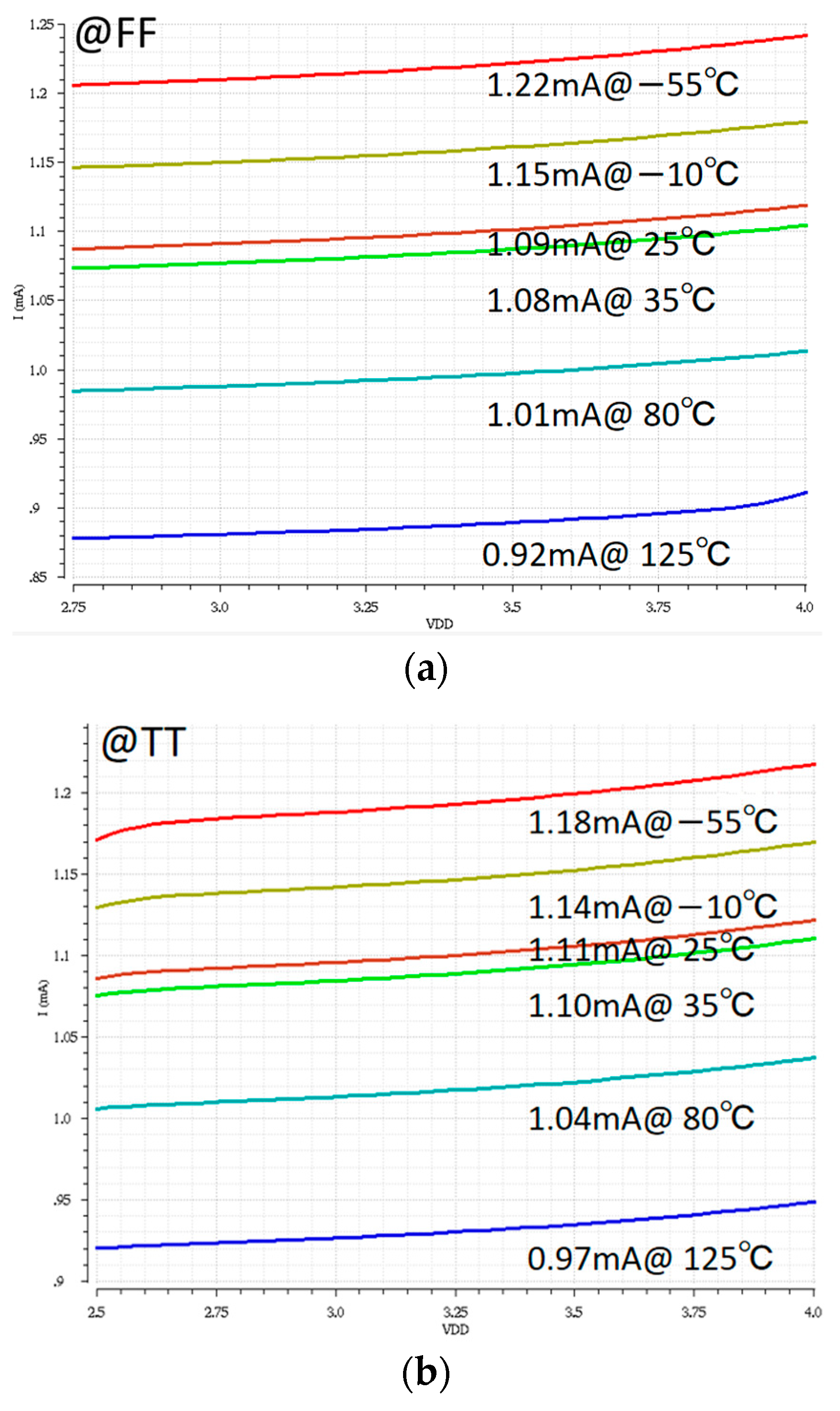
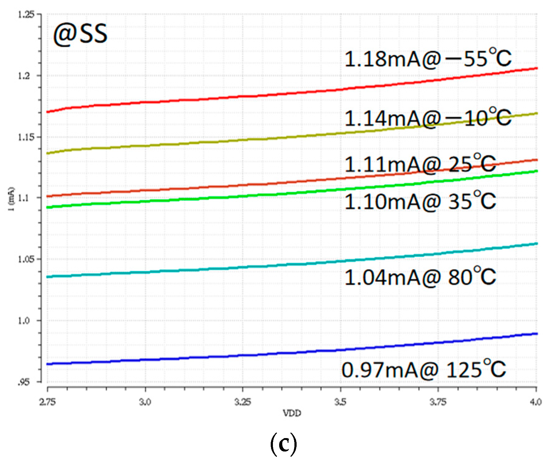
Figure 11 illustrates the simulation results of PVT variations for the bias current of the proposed m-CMVD, where the
x-axis represents the supply voltage varied from 2.75 V to 4.0 V, while the
y-axis depicts the resulting bias currents at different temperatures, from −55 °C to 125 °C.
For the case of FF corners (as shown in
Figure 11a), the largest variation of 4.3% occurs at 125 °C when compared to the reference current of 1.09 mA at 25 °C. For the case of SS corners (as depicted in
Figure 11c), the deviation of 5.4% occurs at 125 °C.
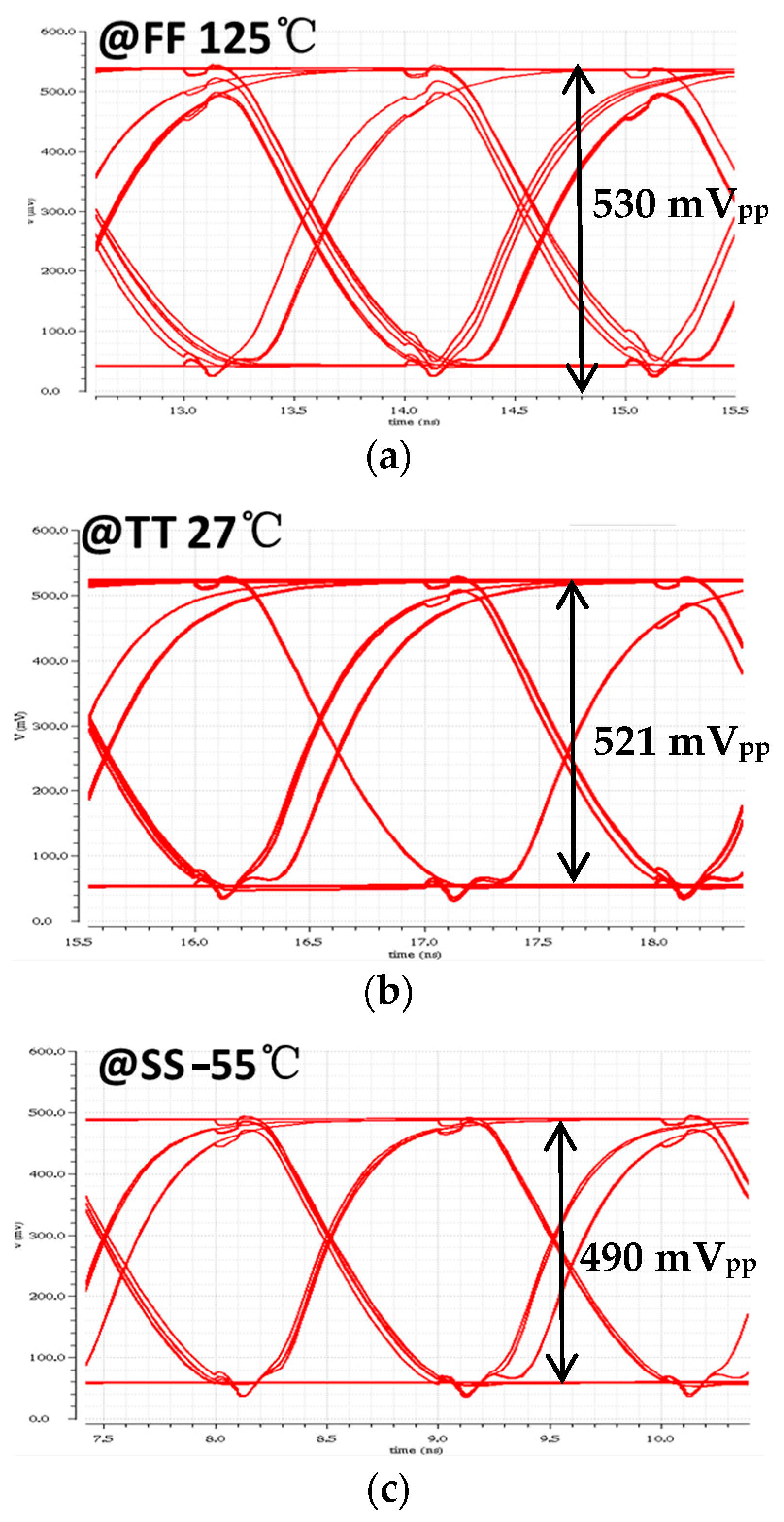
Figure 12 shows the simulated PVT variations of the eye-diagrams for the m-CMVD circuit at the same 1 Gb/s operations with an input current of 10 mA
pp. It is clearly seen that a maximum amplitude deviation of ~6% is observed from the nominal value of 521 mV
pp.
Table 1 compares the performance of the proposed m-CMVD circuit with the previously reported CMOS VCSEL (or laser diode) drivers. Ref. [
9] presented a driver array with multi-channel laser diodes, where each channel generated the modulation currents of 1~16 mA
pp with the bias currents of 1~10 mA. However, it inevitably consumed high power. Ref. [
12] demonstrated a voltage-mode VCSEL driver, in which the eye-diagrams of four channels were optically measured at 10 Gb/s. Yet, the proposed chip utilized dual supplies and consumed a large amount of power. Ref. [
13] realized a differential VCSEL driver with push-pull voltage-mode configuration in a 65 nm CMOS process, which only yielded a limited modulation current of 7 mA. Ref. [
14] suggested a CMOS linear VCSEL driver for intermediate frequency over fiber links, where a large bias current of 10 mA was still required. Ref. [
17] introduced a current-mode VCSEL driver that shared a topology almost similar to this work, with the same bias and modulation currents. However, it yielded the output pulses with severe distortions and peaking. In this work, a modified current-mode CMVD is presented, not only to provide stable bias currents with the regulated cascode current mirror circuit but also to generate variable modulation currents up to 10 mA
pp with the modified CSL circuit, resulting in the absence of pulse distortions and overshoots.
