Abstract
This paper presents an inverter-based active feedback transimpedance amplifier (IAF-TIA), in which an active feedback is applied to a voltage-mode inverter-based TIA, and therefore, the controlled positive regeneration process enables the proposed IAF-TIA to achieve the limiting operations for input currents greater than 100 μApp. However, the active inverter feedback mechanism might be prone to instability, hence mandating a very careful optimization of the loop gain. For this purpose, a diode-connected NMOS transistor is employed as a switch in the feedback path with its gate connected to the input, which helps not only to mitigate the corresponding issue but also to accommodate large input currents up to 1.5 mApp. The proposed IAF-TIA implemented in a standard 180 nm CMOS process demonstrates a 70.5 dBΩ transimpedance gain, 1.21 GHz bandwidth, 4.3 noise current spectral density, 63.5 dB input dynamic range, and 23.6 mW power dissipation from a single 1.8 V supply. The chip core occupies an area of 180 × 50 μm2, including an on-chip P+/N-well/Deep N-well avalanche photodiode as an optical detector.
1. Introduction
For the past few decades, research on transimpedance amplifiers (TIAs) as an analog front-end (AFE) receiver circuit has been extensively conducted along with the proliferation of consumer electronic applications including optical interconnects and LiDAR sensors, because the TIA determines the overall performance of optical receivers in aspects such as their gain, bandwidth, noise, dynamic range, and power [1,2,3,4,5,6,7,8]. Accordingly, novel circuit methodologies are required in the designs of TIAs to satisfy more stringent performance specifications, especially low power for prolonged reliability and small area for low cost.
Conventionally, the voltage-mode shunt feedback inverter TIA has been very popular because of its high gain and low noise characteristics [2,3]. However, there is a well-known disadvantage in this configuration, i.e., the gain–bandwidth tradeoff. In addition, the input dynamic range would be considerably narrow with the high transimpedance gain characteristics, so severe signal distortion might occur for large input photocurrents. Hence, a number of current-mode TIA architectures were suggested, e.g., common-gate TIAs [4,5,6], regulated cascode TIAs [7,8,9,10], current mirror TIAs [11,12], etc. These current-mode TIAs are very effective to isolate the large photodiode capacitance from the bandwidth determination due to its inherently low input impedance. Yet, the notoriously large input noise current spectral density can be problematic so that the exploitation of these current-mode TIAs is limited to short-distance optical interconnects and/or short-range detection for LiDAR sensors.
In this paper, a new architecture of a voltage-mode shunt-feedback inverter TIA is proposed to demonstrate a low-cost, low-power solution that is capable of the limiting operations by applying an active feedback mechanism to a conventional shunt feedback TIA. Thereby, it can extend the dynamic range even with the absence of automatic gain control.
Additionally, a diode-connected NMOS transistor is added as a switch in the feedback path to achieve a wide input dynamic range (i.e., 1.0 mApp to 1.5 mApp in this work) by automatically turning on/off the feedback path.
Meanwhile, as an optical photodetector, either a p-i-n photodiode or an avalanche photodiode (APD) is employed, depending on the specified applications. Provided that the utilized optical photodetector is an off-chip component, however, the bond-wire interconnection between the photodiode and the receiver chip causes significant signal distortions. Also, the length of bond-wires cannot be precisely controlled, thus degrading the receiver performance. Furthermore, on-chip electro-static discharge (ESD) protection diodes are mostly necessary to avoid the chip damage from the ESD, which may shrink the receiver bandwidth. Therefore, in this work, on-chip photodetectors are realized to avoid the aforementioned issues. In particular, an APD is preferred despite the characteristics of noise amplification because the target application of this work is short-range LiDAR sensors where the targets are usually located within a few-meter distance, hence providing large photocurrents.
2. Circuit Description
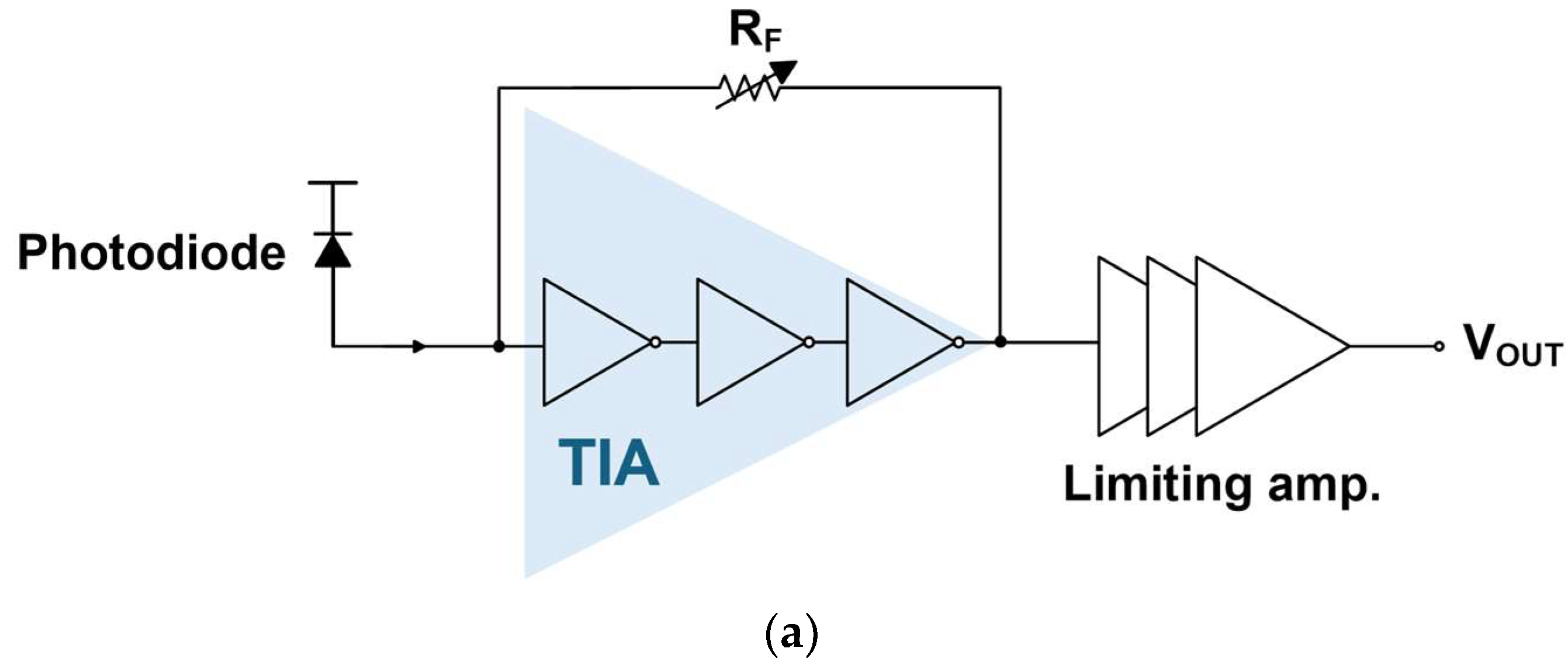
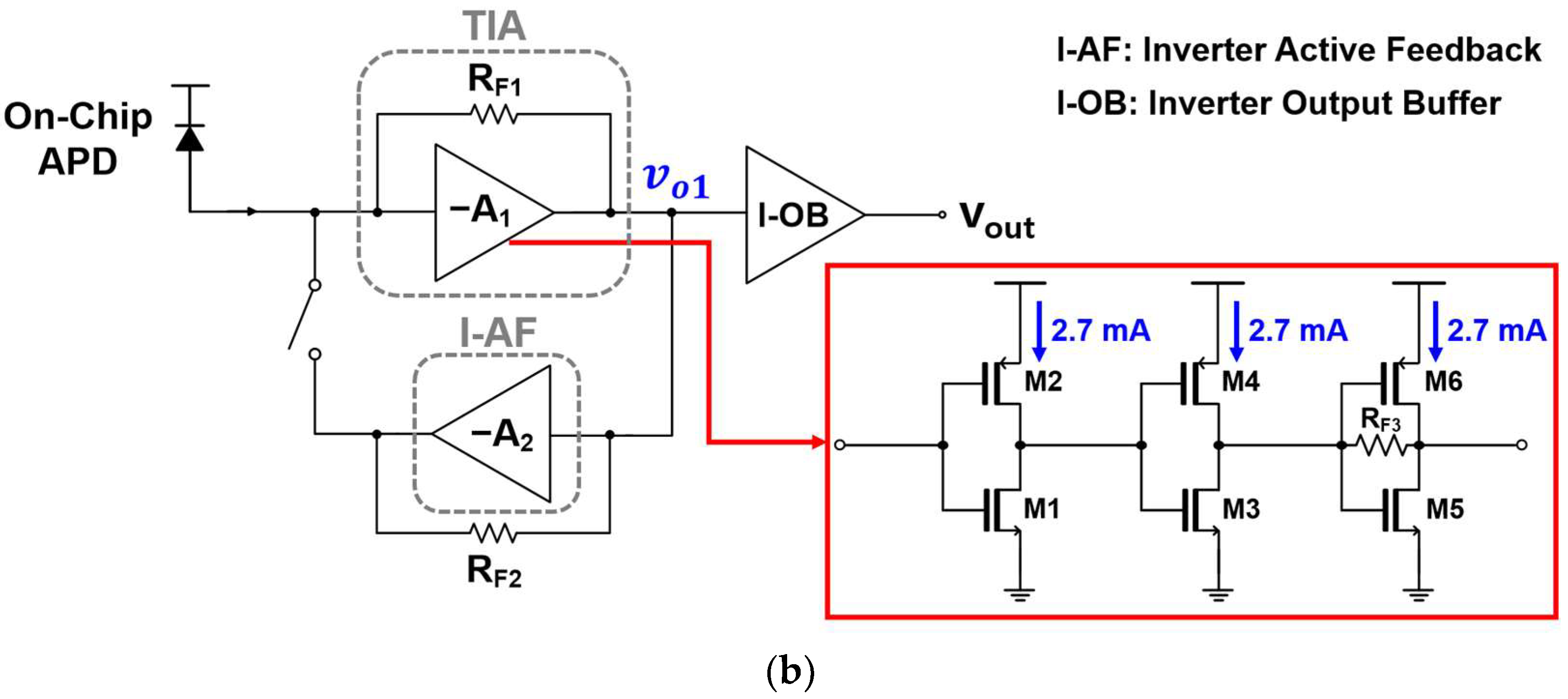
Figure 1a shows the block diagram of a conventional shunt feedback TIA (SF-TIA), and Figure 1b depicts that of the proposed inverter-based active feedback TIA (IAF-TIA). The conventional TIA comprises a three-stage inverter amplifier and an automatic gain control (AGC) circuit with a variable feedback resistor. On the contrary, the IAF-TIA consists of a three-stage cascaded inverter amplifier with dual feedback resistors and an active feedback inverter. Particularly, an NMOS switch is inserted between the input node and the active feedback inverter so that the switch can be turned on for input currents greater than 100 µApp.

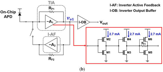
Figure 1.
Block diagrams of (a) a conventional SF-TIA and (b) the proposed IAF-TIA.
Since the active feedback circuit is basically an inverter TIA, the closed-loop mechanism becomes a positive feedback path. Thereby, it might give rise to instability in the proposed IAF-TIA. Thus, a very careful optimization of the closed-loop gain is necessary to prevent the circuit from unstable operations. With the iterations of the optimization process, the proposed IAF-TIA can facilely achieve the limiting operations for input currents greater than 100 µApp despite the absence of the following power-hungry limiting amplifier.
2.1. Multi-Stage Inverter
The shunt feedback inverter TIA is one of the most popular configurations due to its design simplicity, high gain, and low noise. However, it suffers from the notorious gain–bandwidth tradeoff and limited dynamic range, thereby mandating an AGC circuit. Also, the voltage gain in the inverter amplifier directly affects the transimpedance gain characteristics, hence demanding a large voltage gain. Yet, it cannot be increased indefinitely due to the circuit stability. Therefore, a three-stage cascaded inverter amplifier is considered to be the optimized configuration [13].
Meanwhile, Figure 1b shows the block diagram of the proposed multi-stage inverter-based TIA that exploits a dual-feedback topology, where the main feedback (RF1) is applied from the output (vo1) to the input node, and the local feedback (RF3) is inserted at the third inverter stage. Then, the small signal analysis of the IAF-TIA shows that the equations of the input resistance and the transimpedance gain are respectively given by
where A1 represents the voltage gain of the TIA.
Then, it is clearly seen that the input resistance of the proposed IAF-TIA becomes very small, enabling us not only to avoid the loss of the input photocurrents effectively but also to extend the bandwidth further. Provided that the transimpedance gain of the proposed IAF-TIA is identical to that of a conventional SF-TIA, the feedback resistance (RF1) can be enlarged such that the noise contribution from RF1 can become negligible because the noise current spectral density from RF1 is inversely proportional to the resistance. Additionally, the dual-feedback mechanism helps to match the output resistance to the required value, 50 Ω, due to the parallel combination of the main TIA and the I-AF.
2.2. Inverter-Based Active Feedback
Figure 2 depicts a schematic diagram of the proposed inverter-based active feedback (I-AF) circuit that basically functions as a positive feedback path. Then, the output voltages of the IAF-TIA can be easily saturated even with small input photocurrents.
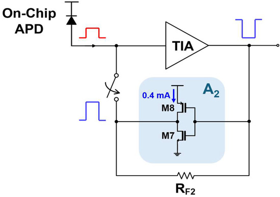
Figure 2.
A schematic diagram of the inverter-based active feedback circuit.
Hence, this configuration helps to eliminate the power-hungry limiting amplifier that is inevitably equipped in a typical optical receiver. Consequently, it results in the potential to achieve a low-power, low-cost solution for the applications of optical interconnects and short-range LiDAR sensors. Namely, the I-AF circuit not only extends the input dynamic range in the transient responses but also removes the limiting operations in a receiver architecture. These will be demonstrated in the simulation and measurement results of the proposed IAF-TIA. Yet, it should be noted that the positive feedback might lead to the regeneration process and is thus prone to oscillations, i.e., instability. In order to avoid these undesired situations, the voltage gain in the feedback inverter should be judiciously selected to be unity.
2.3. Inverter-Based Output Buffer
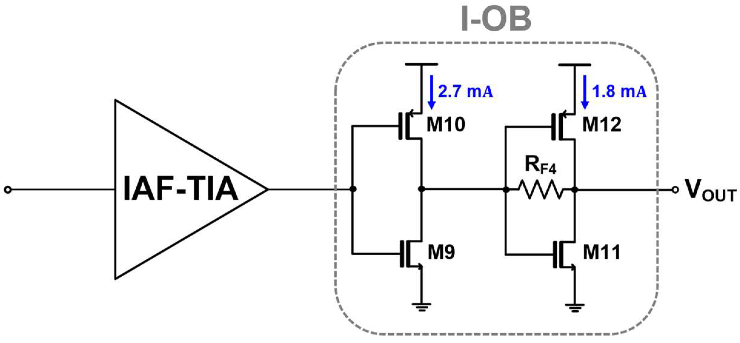
Finally, the inverter-based output buffer (I-OB) is employed to match the output impedance to 50 Ω and also to isolate the output load capacitance from the core TIA circuit effectively. Figure 3 illustrates the schematic diagram of the I-OB that consists of an inverter followed by an additional inverter-based TIA for impedance matching. In this work, the simulated output resistance is determined to be 67.5 Ω.
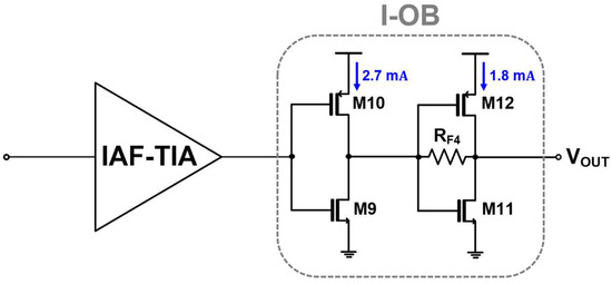
Figure 3.
A schematic diagram of the proposed inverter-based output buffer.
2.4. On-Chip APD
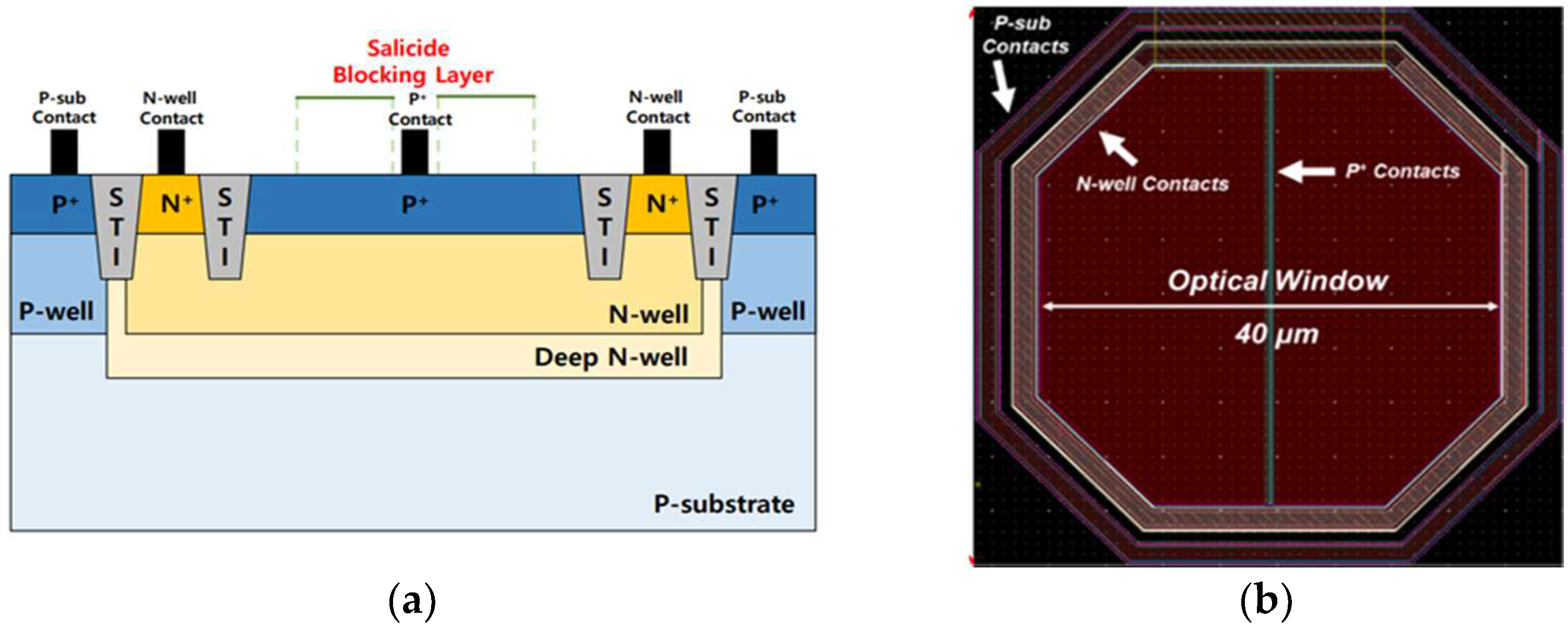
Figure 4a illustrates the cross-sectional view of the on-chip CMOS P+/N-well/Deep N-well APD (or P+/NW/DNW APD), where the avalanche multiplication is initialized by a hole occurring at the P+/NW junction. The premature edge breakdown can be prevented by the shallow trench insulators (STIs). Also, the DNW improves the near-infrared (NIR) sensitivity because it decreases the number of holes spreading into the P-substrate. Moreover, the photocurrents generated in the P-substrate can be excluded owing to the built-in potential barrier between the DNW and the P-substrate.
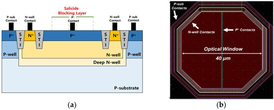
Figure 4.
(a) A cross-sectional view of a P+/NW/DNW APD, (b) the layout of the on-chip APD.
Figure 4b depicts the layout of the on-chip CMOS P+/NW/DNW APD, where the P+ source and drain regions should be covered by the salicide blocking layer to form an optical window.
However, the P+ contacts in the middle of the optical window should not be blocked because the salicidation process reduces the contact’s resistivity [14]. The diagonal length of the optical window is 40 µm, such that the APD provides a total depletion capacitance (CPD) of 470 fF and a photodetection bandwidth of 1.7 GHz at a reverse bias of 10.25 V. The octagonal shape is preferred to minimize the possible damage from the edge breakdown. For HSPICE simulation purposes, the equivalent modeling of the on-chip APD comprises an ideal current source with a parasitic capacitance of 470 fF.
3. Layout and Simulation Results
Figure 5 illustrates the layout of the proposed IAF-TIA with an on-chip P+/NW/DNW APD, where the chip core occupies an area of 180 × 50 μm².

Figure 5.
The layout of the proposed IAF-TIA.
Post-layout simulations were conducted for the IAF-TIA by utilizing the model parameters of a standard 180 nm CMOS technology. DC simulations reveal that the proposed IAF-TIA dissipates 23.6 mW from a single 1.8 V supply.
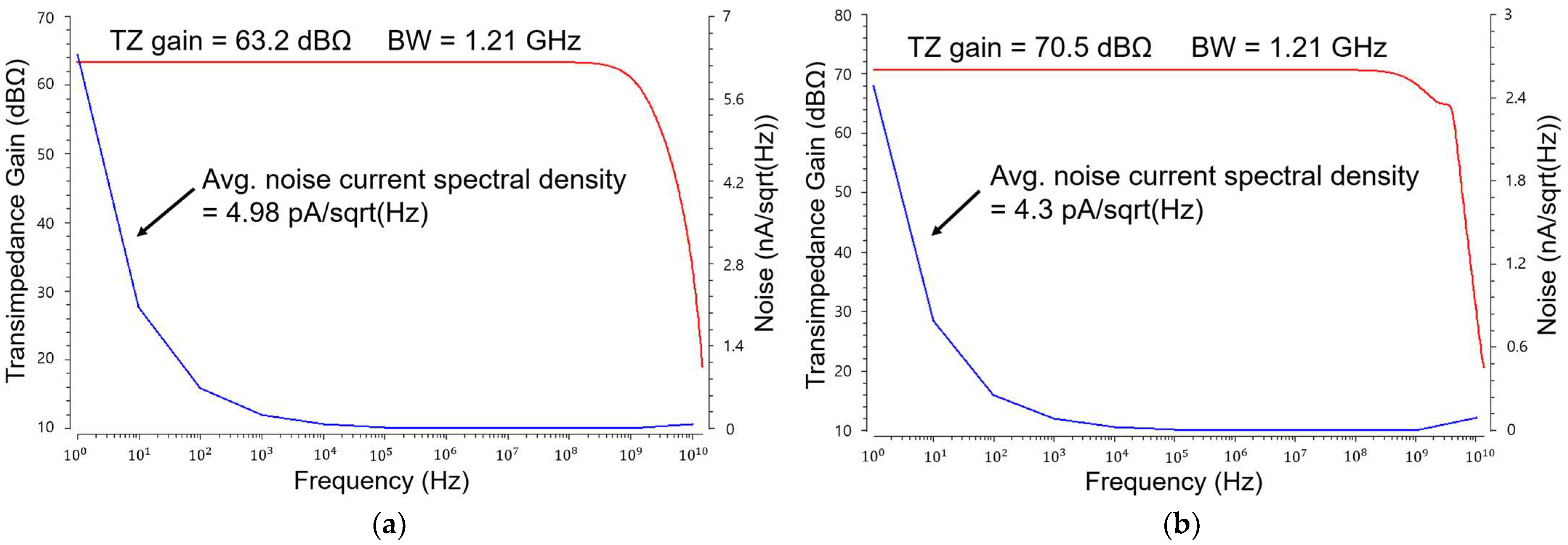
Figure 6 compares the frequency response of the IAF-TIA with that of the conventional SF-TIA for the same bandwidth characteristics, in which the IAF-TIA shows a transimpedance gain of 70.5 dBΩ, a bandwidth of 1.21 GHz for a photodiode capacitance of 0.47 pF (extracted from the on-chip APD in [14,15]), and a noise current spectral density of 4.3 pA/sqrt(Hz). On the contrary, the conventional SF-TIA obtains a transimpedance gain of 63.2 dBΩ, a bandwidth of 1.21 GHz for the same photodiode capacitance of 0.47 pF, and a noise current spectral density of 4.98 pA/sqrt(Hz). Hence, it is clearly seen that the proposed IAF-TIA achieves higher transimpedance gain and lower noise characteristics, as anticipated in the above analysis. In addition, the post-layout simulations reveal that the phase margin of the IAF-TIA is close to 90 deg., which confirms that the proposed IAF-TIA circuit is stable.
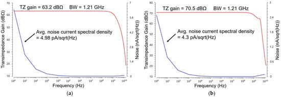
Figure 6.
Simulated frequency responses of (a) the conventional SF-TIA and (b) the proposed IAF-TIA for the same bandwidth characteristics.
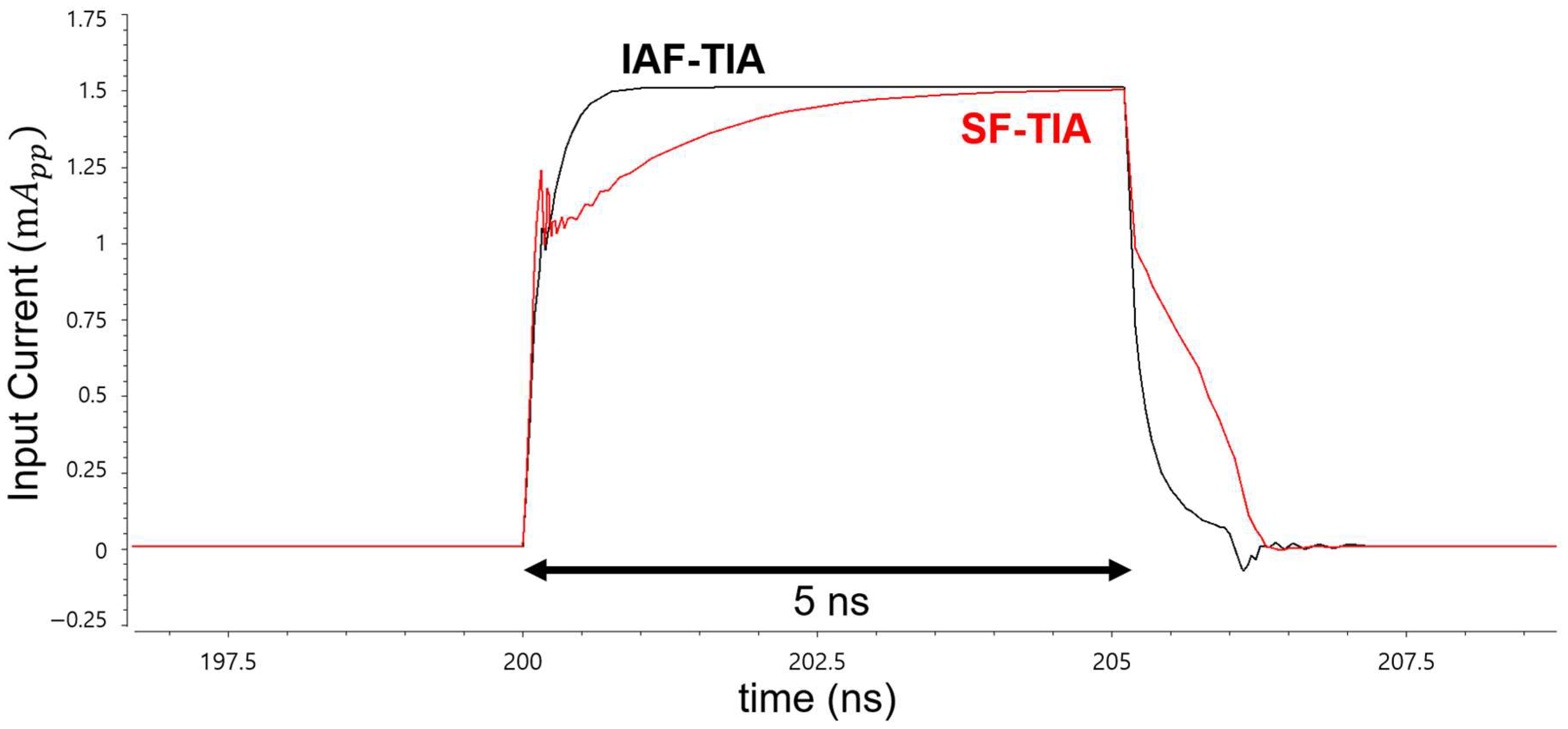
Figure 7 compares the simulated pulse response to the input currents at the IAF-TIA with those at the SF-TIA, where it is clearly seen that the input current pulse of the SF-TIA is severely distorted at both the rising and falling edges. This may be attributed to the limited dynamic range characteristics of the conventional SF-TIA. On the contrary, the proposed IAF-TIA shows an undistorted clean pulse response, thus confirming the extended dynamic range, as anticipated.
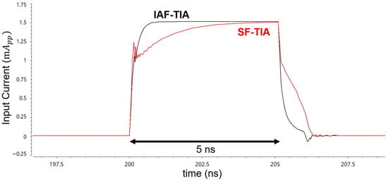
Figure 7.
Simulated current pulses at the input node of the IAF-TIA vs. those of SF-TIA (pulse width: 5 ns).
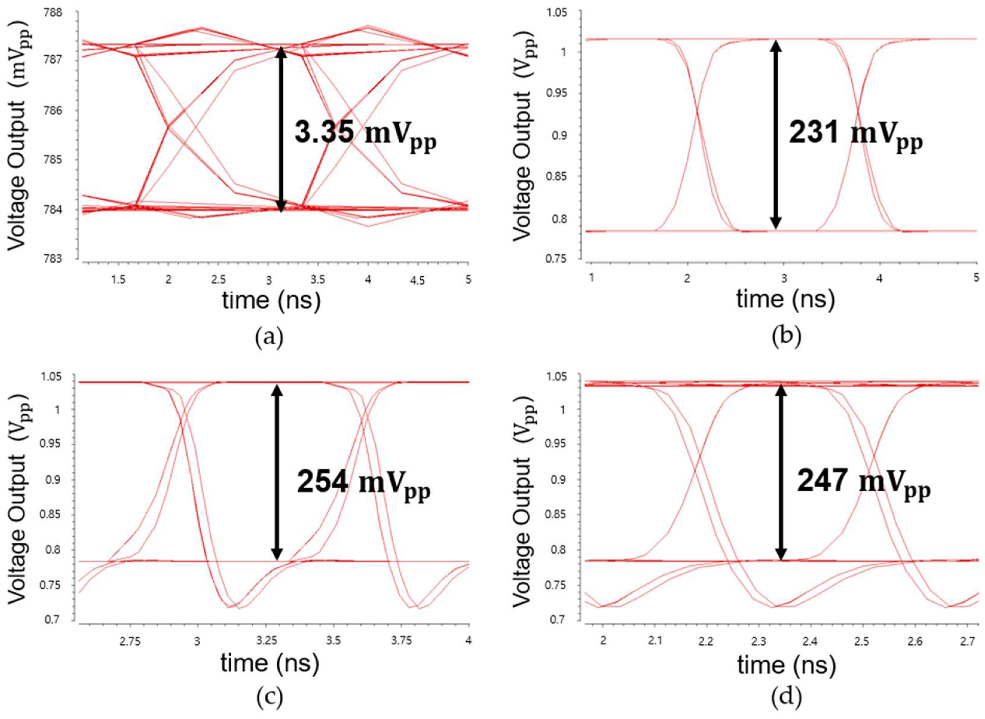
Figure 8 depicts the simulated eye diagrams of the IAF-TIA at the same 300 Mb/s data rate for different input currents from 1 µApp to 1.5 mApp, revealing wide and clean eyes for the wide range of input currents. The overshoot occurs vividly at the falling edges of the eye diagrams for input currents greater than 500 µApp, which may be attributed to the active positive feedback path. Yet, it is clearly seen that the eye heights are saturated from input currents larger than 100 µApp.
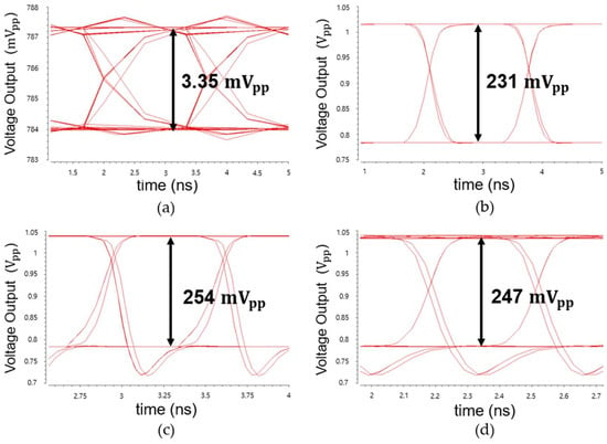
Figure 8.
Simulated eye diagrams of the IAF-TIA at 300 Mb/s data rates: (a) 1 μApp, (b) 100 μApp, (c) 500 μApp, and (d) 1.5 mApp, respectively.
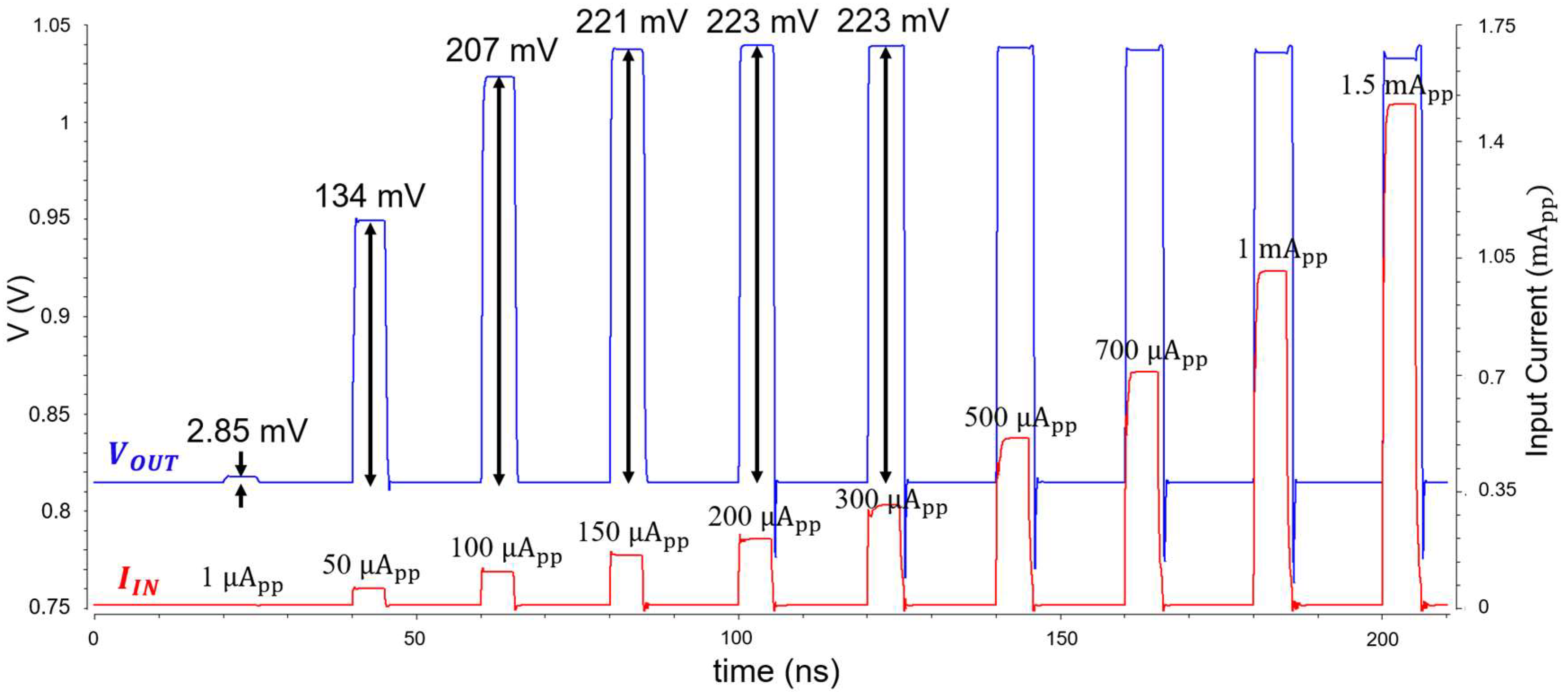
Figure 9 shows the simulated pulse response of the IAF-TIA, where the output pulses for small input currents less than 100 µApp increase almost linearly, while those for large photocurrents greater than 100 µApp are saturated. Thus, it confirms the extended dynamic range and the limiting operations for large input currents.
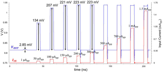
Figure 9.
The simulated pulse response of the IAF-TIA for different input currents.
Table 1 lists the performance deviation from the process, voltage, temperature (PVT) variations for the three worst cases: (a) SS, 1.62 V, −45 °C, (b) TT, 1.8 V, 25 °C, and (c) FF, 1.98 V, 125 °C, respectively. It is clearly seen that the TZ gain varies within 2%, the bandwidth changes less than 7%, and the noise current spectral density deviates within 14%. In the transient response of the IAF-TIA, the output voltage swing varies within 26% for input currents less than 100 µApp, while the output voltages are saturated for input currents larger than 100 µApp. In addition, the multi-stage architecture of the proposed IAF-TIA might give rise to an offset voltage problem. Therefore, the DC voltage especially at the output node of the IAF-TIA, i.e., Vo1,DC shown in Figure 1b, should be as constant as possible. However, the double-feedback configuration is more efficient to keep the DC bias point because both the main feedback resistor (RF1) and the local feedback resistor (RF3) in the last stage maintain the common-mode DC voltage. Simulations confirm that the DC bias alters within 11.7%.

Table 1.
The PVT simulation results of the proposed IAF-TIA.
Table 2 compares the performance of the proposed IAF-TIA with some of the previously reported CMOS TIAs.

Table 2.
Performance comparison with previously reported TIAs.
The authors of ref. [16] suggested a voltage-mode CMOS feedforward (VCF) input configuration followed by a post-amplifier, which could successfully attain high transimpedance gain and wide dynamic range. However, the AGC function was manually carried out with a reference voltage. Also, a commercial 16-channel off-chip APD array was exploited.
The authors of ref. [17] suggested a current mirror input configuration with a shunt feedback topology, which could successfully attain high transimpedance gain and wide dynamic range. However, the AGC function was carried out by an external field programmable gate array. Also, it exploited off-chip APDs with a very high 45 A/W responsivity.
The authors of ref. [18] presented a frequency-compensated inverter TIA that could demonstrate very low noise current spectral density. However, it revealed high power dissipation and mandated a large reverse voltage of 200 V for the off-chip APD to achieve 50 A/W responsivity characteristics.
The authors of ref. [19] succeeded in realizing a fully differential TIA to improve the PSRR characteristics. For this purpose, a dual-feedback folded cascode input configuration was suggested with an active single-to-differential converter to minimize the mismatches. Also, a following cascaded post-amplifier was necessary, hence leading to a rather large power consumption.
In this proposed IAF-TIA, we realized the inverter-based positive feedback AGC mechanism with an NMOS switch in the feedback path by judiciously selecting the loop gain. Also, the dual-feedback topology enables us to equip a large feedback resistor in the TIA, thereby reducing the noise current spectral density despite the relatively wide bandwidth characteristics. Consequently, the input dynamic range of the proposed IAF-TIA can be extended much further, i.e., the minimum and maximum detectable currents of 1 μApp and 1.5 mApp, respectively.
4. Conclusions
This paper presents a novel inverter-based active-feedback TIA realized in a standard 180 nm CMOS process. Due to the additional inverter TIA in the feedback path, the IAF-TIA can limit the output voltage swings by the regeneration process and therefore enable us to discard the following power-hungry limiting amplifier. Conclusively, the proposed IAF-TIA demonstrates the potential to acquire a low-power, low-cost solution for optical interconnects and LiDAR sensors.
Author Contributions
Conceptualization, S.-M.P.; methodology, S.P. and S.-M.P.; validation, S.P., S.L., B.S., Y.C. (Yejin Choi), Y.S., Y.C. (Yeojin Chon) and S.C.; writing—original draft preparation, S.P., S.L., B.S. and S.-M.P.; writing—review and editing, S.P., S.L., B.S., Y.C. (Yejin Choi), Y.S., Y.C. (Yeojin Chon) and S.C.; visualization, S.P., S.L. and B.S.; supervision, S.-M.P.; project administration, S.-M.P.; funding acquisition, S.-M.P. All authors have read and agreed to the published version of the manuscript.
Funding
This research was supported by the MSIT (Ministry of Science and ICT), Republic of Korea, under the ITRC (Information Technology Research Center) support program (IITP-2020-0-01847) supervised by the IITP (Institute for Information and Communications Technology Planning and Evaluation).
Institutional Review Board Statement
Not applicable.
Informed Consent Statement
Not applicable.
Data Availability Statement
Data are contained within the article.
Acknowledgments
This work was supported by the National Research Foundation (NRF), Korea, under project BK21 FOUR. The EDA tool and chip fabrication were supported by the IC Design Education Center.
Conflicts of Interest
The authors declare no conflicts of interest.
References
- Lakshmikumar, K.R.; Kurylak, A.; Nagaraju, M.; Booth, R.; Nandwana, R.K.; Pampanin, J.; Boccuzzi, V. A Process and Temperature Insensitive CMOS Linear TIA for 100 Gb/s/λ PAM-4 Optical Links. IEEE J. Solid-State Circuits 2019, 11, 3180–3190. [Google Scholar] [CrossRef]
- Razavi, B. Design of Integrated Circuits for Optical Communications, 2nd ed.; Wiley: Hoboken, NJ, USA, 2012. [Google Scholar]
- Andrade, H.; Maharry, A.; Hirokawa, T.; Valenzuela, L.; Pinna, S.; Simon, S.; Schow, C.L.; Buckwalter, J.F. Analysis and Monolithic Implementation of Differential Transimpedance Amplifiers. IEEE J. Light. Technol. 2020, 38, 4409–4418. [Google Scholar] [CrossRef]
- De Medeiros Silva, M.; Oliveira, L.B. Regulated common-gate transimpedance amplifier designed to operate with a silicon photo-multiplier at the input. IEEE Trans. Circuits Syst. I Regul. Pap. 2013, 61, 725–735. [Google Scholar] [CrossRef]
- Elsaegh, S.; Veit, C.; Zschieschang, U.; Amayreh, M.; Letzkus, F.; Sailer, H.; Jurisch, M.; Burghartz, J.N.; Wurfel, U.; Klauk, H.; et al. Low-power organic light sensor array based on active-matrix common-gate transimpedance amplifier on foil for imaging applications. IEEE J. Solid-State Circuits 2020, 55, 2553–2566. [Google Scholar] [CrossRef]
- Lu, Z.; Yeo, K.S.; Lim, W.M.; Do, M.A.; Boon, C.C. Design of a CMOS Broadband Transimpedance Amplifier with Active Feedback. IEEE Trans. Very Large Scale Integr. (VLSI) Syst. 2010, 18, 461–472. [Google Scholar] [CrossRef]
- Park, S.M.; Yoo, H.-J. 1.25-Gb/s regulated cascode CMOS transimpedance amplifier for Gigabit Ethernet applications. IEEE J. Solid-State Circuits 2004, 39, 112–121. [Google Scholar] [CrossRef]
- Costanzo, R.; Bowers, S.M. A current reuse regulated cascode CMOS transimpedance amplifier with 11-GHz bandwidth. IEEE Microw. Wirel. Comp. Lett. 2018, 28, 816–818. [Google Scholar] [CrossRef]
- Takahashi, Y.; Ito, D.; Nakamura, M.; Tsuchiya, A.; Inoue, T.; Kishine, K. Low-Power Regulated Cascode CMOS Transimpedance Amplifier with Local Feedback Circuit. Electronics 2022, 11, 854. [Google Scholar] [CrossRef]
- Li, C.; Palermo, S. A Low-Power 26-GHz Transformer-Based Regulated Cascode SiGe BiCMOS Transimpedance Amplifier. IEEE J. Solid-State Circuits 2013, 48, 1264–1275. [Google Scholar] [CrossRef]
- Yoon, D.; Joo, J.E.; Park, S.M. Mirrored Current-Conveyor Transimpedance Amplifier for Home Monitoring LiDAR Sensors. IEEE Sens. J. 2020, 21, 5589–5597. [Google Scholar] [CrossRef]
- Zohoori, S.; Dolatshahi, M.; Pourahmadi, M.; Hajisafari, M. A CMOS, low-power current-mirror-based transimpedance amplifier for 10 Gbps optical communications. Microelectron. J. 2018, 80, 18–27. [Google Scholar] [CrossRef]
- Yan, P.; Hong, C.; Chang, P.-H.; Kang, H.; Annabattuni, D.; Kumar, A.; Fan, Y.-H.; Liu, R.; Rady, R.; Palermo, S. A 12.5 Gb/s 1.38 mW all-inverter-based optical receiver with multi-stage feedback TIA and continuous time linear equalizer. Analog. Integr. Circuits Signal Process. 2024, 119, 283–296. [Google Scholar] [CrossRef]
- Lee, M.-J.; Choi, W.-Y. Performance comparison of two types of silicon avalanche photodetectors based on N-well/P-substrate and P+/N-well junctions fabricated with standard CMOS technology. J. Opt. Soc. Korea 2011, 15, 1–3. [Google Scholar] [CrossRef]
- Hu, Y.; Joo, J.-E.; Zhang, X.; Chon, Y.; Choi, S.; Lee, M.-J.; Park, S.-M. A Current-Mode Optoelectronic Receiver IC for Short-Range LiDAR Sensors in 180 nm CMOS. Photonics 2023, 10, 746. [Google Scholar] [CrossRef]
- Hong, C.; Kim, S.-H.; Kim, J.-H.; Park, S.M. A linear-mode LiDAR sensor using a multi-channel CMOS transimpedance amplifier array. IEEE Sens. J. 2018, 18, 7032–7040. [Google Scholar] [CrossRef]
- Zheng, H.; Ma, R.; Liu, M.; Zhu, Z. High Sensitivity and Wide Dynamic Range Analog Front-End Circuits for Pulsed TOF 4-D Imaging LADAR Receiver. IEEE Sens. J. 2018, 18, 3114–3124. [Google Scholar] [CrossRef]
- Wang, X.; Ma, R.; Li, D.; Zheng, H.; Liu, M.; Zhu, Z. A low walk error analog front-end circuit with intensity compensation for direct ToF LiDAR. IEEE Trans. Circuits Syst. I Regul. Pap. 2020, 67, 4309–4321. [Google Scholar] [CrossRef]
- Joo, J.-E.; Lee, M.-J.; Park, S.M. A CMOS Fully Differential Optoelectronic Receiver for Short-Range LiDAR Sensors. IEEE Sens. J. 2023, 23, 4930–4939. [Google Scholar] [CrossRef]
Disclaimer/Publisher’s Note: The statements, opinions and data contained in all publications are solely those of the individual author(s) and contributor(s) and not of MDPI and/or the editor(s). MDPI and/or the editor(s) disclaim responsibility for any injury to people or property resulting from any ideas, methods, instructions or products referred to in the content. |
© 2024 by the authors. Licensee MDPI, Basel, Switzerland. This article is an open access article distributed under the terms and conditions of the Creative Commons Attribution (CC BY) license (https://creativecommons.org/licenses/by/4.0/).

