Communication

Plasmonic Focusing of a High-Order Cylindrical Vector Beam for On-Chip Detection

1
School of Optical-Electrical and Computer Engineering, University of Shanghai for Science and Technology, Shanghai 200093, China
2
Zhangjiang Laboratory, Shanghai 201204, China
*
Author to whom correspondence should be addressed.
Photonics 2024, 11(6), 579; https://doi.org/10.3390/photonics11060579
Submission received: 17 May 2024 / Revised: 14 June 2024 / Accepted: 19 June 2024 / Published: 20 June 2024
(This article belongs to the Section Optical Interaction Science)

Abstract

:
We investigate the interaction between cylindrical vector beams (CVBs) and metallic annular structures. The mechanisms for plasmonic focusing and field distributions are studied both analytically and numerically. We demonstrate that the focusing patterns are locked with the order of CVBs due to the polarization selectivity for the excitation of plasmonic fields, which can be employed as a simplified yet efficient means of characterizing and detecting CVBs. The robustness of the focusing pattern is analyzed as a deviation between the centers of the CVBs and nanoring is introduced, providing a quantitative indicator of the relationship between the maximum deviation value and the focusing patterns. Our research contributes to a deeper understanding of interactions between CVBs and nanostructures, paving the way for novel applications in light detection and optical imaging.

1. Introduction

Polarization is one of the fundamental properties of light and plays a crucial role in many areas of modern science and technology [1,2,3]. Vector beams with spatially variant polarization states have attracted considerable research interest for the past decades due to their customized intensity patterns and novel applications. As a sophisticated class of structured light, cylindrical vector beams (CVBs) exhibit cylindrical symmetry in their polarization with a singularity and donut-shaped intensity pattern at the center. A significant characteristic of CVBs is the additional degree of freedom in terms of their vectorial polarization order, with different states being orthogonal to each other, where radially and azimuthally polarized beams are the two lowest orders of CVBs. High-order vectorial polarization states have also been widely investigated [4,5]. In contrast to the conventional linearly polarized beam, CVBs possess strong longitudinal/transverse field components in focusing [6,7,8,9,10], giving rise to many intriguing phenomena such as spin–orbit interaction [11], optical needles [12], and the topological structure of light [13,14,15,16,17], as well as a variety of applications including optical trapping [18,19,20,21], optical lithography [22,23], and optical micro-fabrication [24,25].
The unique polarization structure of CVBs opens up new avenues for light manipulation and optical engineering at the subwavelength scale since tailored polarization distributions can selectively couple with the resonant modes of nanostructures [26,27]. Particularly, the interaction between CVBs and metallic nanostructures has drawn much research attention. By tuning the polarization state of CVBs, researchers can manipulate the plasmonic resonances, leading to enhanced field localization, chiroptical effects, and nonlinear optical effects [28,29,30]. The selective excitation of plasmonic modes has promoted the development of on-chip photonic devices for advanced nanophotonic technologies with tailored functionalities [31,32]. Many plasmonic devices were proposed to focus surface waves and detect the polarization order of CVBs [33,34,35,36,37], which play a significant role in ultrasensitive sensing [38,39], nonlinear optics [40], and quantum information processing [41,42,43], further highlighting the need for robust methods to both measure and analyze the features of high-order vector beams.
In this work, we investigated the plasmonic focusing patterns generated by the interaction between high-order cylindrical vector beams and metallic annular structures. We demonstrated that the number of focusing lobes is related to the order of the CVBs, which stems from the polarization selectivity for the excitation of plasmonic fields. The robustness of the focusing pattern is analyzed as a deviation between the center of the CVBs, and nanoring is introduced. Our results suggest that the plasmonic patterns can serve as a candidate for a simplified yet efficient means of characterizing and detecting CVBs, potentially leading to the development of CVB-centric information detection systems. Moreover, this model could be employed as a precise calibration methodology within sophisticated optical imaging systems, thereby allowing for improved accuracy and reliability in mapping and manipulating the features of CVB fields.

2. Theoretical Model for Ideal Alignment

The schematic illustration for generating plasmonic focusing patterns is shown in Figure 1a. A metallic nanoring with an inner radius r 0 = 7   μ m is etched into a gold film ( n A u = 0.18 + 3.06 i at 633 nm) of 200 nm thickness deposited on a glass substrate (n = 1.515). An incident CVB with a wavelength of λ = 633 nm illuminates the metallic nanostructure perpendicularly from the glass side. To investigate the transmission properties under the subwavelength regime ( λ / d > 1 ) [44,45,46], the slit width is set to be significantly smaller than the incident wavelength ( d = 200   n m ). The subwavelength dimensions of the annular ring structure facilitate momentum matching between the incident light and the surface plasmon polariton (SPP), enabling the excitation and confinement of surface waves. The annular ring operates as a nanoantenna, coupling the incident-free space beam to SPPs propagating along the surface.
Our analysis initiates with the premise that the incident light is precisely centered atop the metallic ring, ensuring no discrepancy between their respective centers. The geometric layout employed for calculation is depicted in Figure 1b. Given this supposition, incident CVBs, defined by their order m and an initial phase ϕ 0 , can be represented by the Jones vector as follows:
E i n = cos m ϕ + ϕ 0 e x sin m ϕ + ϕ 0 e y
For a slot of sufficiently narrow dimensions, solely the radial component of incident CVB’s electric field is capable of coupling with and stimulating SPP excitation [47,48]. The polarization states of the incident light can be formulated in the cylindrical coordinate system as follows:
E = e i m 1 ϕ + ϕ 0 + e i m 1 ϕ + ϕ 0 2 e r + e i m 1 ϕ + ϕ 0 e i m 1 ϕ + ϕ 0 2 i e ϕ
Equation (2) implies that a CVB can be regarded as the superposition of radially and azimuthally polarized vortex beams with the topological charge determined by the order of CVB. As an arbitrary order, CVB illuminates on the annular ring; it induces two optical vortices of opposite topological charges, which then engage with the metallic nanoslit to produce plasmonic vortices. Since the z component of SPP is dominant, the fields excited at any arbitrary position ( R , θ ) relative to the central point can be expressed as follows:
E z = E 0 z e i m 1 ϕ + ϕ 0 + e i m 1 ϕ + ϕ 0 2 e k z z e i k s p p R e R r e r r d ϕ
where E 0 z signifies the amplitude of the electric field, k s p p and k z are the transverse and longitudinal wavevectors of plasmonic field. Since the propagation direction of SPP at each segment of slot is pointing to the origin, the wavevector of SPP can be expressed as k s p p = k s p p e r , guiding directly to the formulation of Equation (3) stated below:
E z = E 0 z e k z z r e i k s p p r e i m 1 ϕ + ϕ 0 + e i m 1 ϕ + ϕ 0 2 e i k s p p R c o s θ ϕ ϕ = π E 0 z e k z z r e i k s p p r e i m 1 θ + ϕ 0 i m 1 J m 1 k s p p R + e i m 1 θ + ϕ 0 i m 1 J 1 m k s p p R
where J l is the Bessel function of the first kind with order l . Equation (4) reveals that the focusing pattern of CVB is a result of two plasmonic vortices with opposite topological charges. By applying the symmetry of Bessel functions that J l ( x ) = 1 l J l ( x ) , the description of the focusing pattern can consequently be framed as follows:
E z R ,   θ e i m 1 θ + ϕ 0 i m 1 J m 1 k s p p R + e i m 1 θ + ϕ 0 i m 1 J m 1 k s p p R cos m 1 θ + ϕ 0 J m 1 k s p p R
The equation encompasses a cosine term and m 1 order Bessel function with respect to position parameters R and θ , thereby imparting periodic and symmetric characteristics to the plasmonic fields. We fix the initial phase ϕ 0 to 0 since it only modulates the relative intensity of the focusing field without altering the focusing pattern. Specifically, when m equals 1—indicative of a radially polarized beam—the nanoring transforms the CVB into a zeroth-order evanescent Bessel beam, featuring a prominent central peak (see Figure 2a). Conversely, for the other order of CVBs, polarization selectivity leads to partial coupling of the incident light with SPPs, giving rise to multiple focal points and the central dark plasmonic field. In addition, the number of focusing lobes is locked with the order of CVBs.
The normalized intensity distributions of plasmonic fields of different orders are illustrated in Figure 2a–c. As expected, the number of focuses aligns with the order of incident CVB, where different orders of Bessel profiles are divided along the radial direction, demonstrating the polarization selectivity of the plasmonic lens. With increasing m , the annular plasmonic pattern is further subdivided, which can be employed as a simplified yet efficient means of characterizing and detecting CVBs.

3. Analysis of Focusing with Deviation

As an offset between the center of the CVB and nanoring is introduced, the focusing pattern is modulated. Due to the circular symmetry of the ring structure, we specify the offset in the y direction. Figure 1c shows the geometric configuration. Two different coordinate systems are labeled. The point O represents the geometric center of the nanoring, and the point O represents the illumination center. Due to the mismatch between the geometric center and the incidence center, the radial component of the incidence CVB in the x - y coordinate system is not applicable to the nanoring structure; thus, we need to convert it into the x - y coordinate system. Defining the offset distance as e = | O O | , the incident field for the excitation of the plasmonic field can be expressed as
E = cos m ϕ 1 e x + sin m ϕ 1 e y = cos m ϕ 1 cos ϕ e r sin ϕ e ϕ + sin m ϕ 1 sin ϕ e r + cos ϕ e ϕ = cos m ϕ 1 ϕ e r + sin m ϕ 1 ϕ e ϕ
where ϕ and ϕ 1 are the deviation angle with respect to the geometric center and the incidence point (Figure 1c). From Equation (6), we identify the radial component that excites SPPs as E r = cos m ϕ 1 ϕ , which is different from the case in Section 2. It is related to two geometric parameters. As the offset changes, even for the same point, the deviation angle ϕ changes, causing a modulation of the radial component. It suggests that the plasmonic field will be modulated by the offset value. The field distribution at an arbitrary position ( R , θ ) with respect to the origin is the integral of the field due to the infinitesimal length dl along the ring, which can be expressed as
E z R ,   θ = 0 2 π E 0 z cos m ϕ 1 ϕ e k z z e i k s p p R e R r e r r ϕ = E 0 z e k z z r e i k s p p r 0 2 π cos m 1 ϕ + m α e i k s p p R c o s ϕ θ ϕ
where the geometric relations ϕ 1 = ϕ + α and sin α = e r cos ϕ 1 are used. To facilitate the analysis and obtain insights into its properties, we introduce an approximation based on the assumption that the deviation e is not comparable to the radius of annular ring that e < < r and α   ~   0 . This approximation is valid in two scenarios:
  • The offset value e remains constant, and the angle ϕ 1 is close to π / 2 , which corresponds to observation points located closer to the upper and lower regions of the ring, where the deviation from ideal alignment is minimal.
  • The angle ϕ 1 remains constant, and the offset e is small. This scenario reflects the intuitive understanding that a smaller offset ensures greater focusing accuracy, as the deviation from the alignment is minimized.
Under the small-angle approximation, we can rewrite Equation (7) into the following:
E z R ,   θ 0 2 π c o s m 1 ϕ m e r cos ϕ sin m 1 ϕ   e i k s p p r e i k s p p R c o s ϕ θ r ϕ
Equation (8) reveals that the field distribution can be decomposed into two parts. The first part represents the field distribution in the absence of any offset, corresponding to the ideal alignment scenario. The second part encapsulates the influence of the offset characterized by the term m e r , which depends on both the order of CVB and the relative deviation distance e / r . By utilizing the Bessel integral, the plasmonic field can be expressed as follows:
E z R ,   θ cos m 1 θ J m 1 k s p p R m e 2 r i sin m θ J m k s p p R + m e 2 r i sin m 2 θ J m 2 k s p p R
which is a linear combination of three Bessel functions of different orders: m 1 , m , and m 2 . Notably, in the absence of deviation where e = 0 , which signifies ideal alignment between the CVB center and the nanoring center, the electric field in Equation (9) corresponds to the case of ideal alignment. However, the introduction of deviation introduces distortions into the field distribution. As e increases, these distortions become more pronounced, ultimately leading to a significant alteration of the focusing pattern. For a given CVB with order m, there exists a critical deviation value beyond which the focus pattern becomes indistinguishable, effectively hindering the accurate detection and characterization of the incident CVB. This critical deviation represents the maximum deviation range for the specific device configuration.
The focusing patterns for different deviation distances with m = 4 are shown in Figure 3. At ideal alignment ( e = 0 ), the focusing pattern exhibits a symmetrical distribution with six lobes (Figure 3a). When the deviation is not comparable to the radius of the annular ring, the focusing patterns remain largely unchanged (Figure 3b,c), where the theoretical prediction in Equation (9) agrees well with the simulations (insets in Figure 3b,c). As e increases, the symmetry is progressively broken, leading to more complex electric field distributions (Figure 3d–f), which stem from the mismatched excitation of plasmonic modes due to the offset. The modulation of the focusing patterns in Figure 3d–f is negligible near the y axis, while it is amplified near the x axis. This discrepancy can be explained by the fact that the deviation angle α is smaller for observation points closer to the vertical center boundary of the ring compared to those near the horizontal boundary. Consequently, the approximation in Equation (9) is more accurate in regions where α is inherently smaller. Nevertheless, in most cases, the approximation formula serves as a valuable tool for analyzing related problems.
As the deviation distance e increases, the innermost focuses, which we refer to as the “indicator” due to their distinct characteristics as information indicators for the incident CVB, undergo significant modulations. They become elongated and skewed, with the intensity pattern becoming distorted, hindering the exact extraction of information from the focusing pattern. Simultaneously, extra focal points arise at locations further away from the nanoring center, while the inner focuses become increasingly obscured and distorted. Moreover, the inner horizontal focuses gradually shift towards the left and right extremities of the pattern.
Analyzing the evolution trend depicted in Figure 3, we propose the following judgment criteria to determine the critical deviation value: We measure the intensity distribution and use a certain scale to filter the focus patterns to detect the number of focal points. We observed that, as the “indicator” is distorted, additional focal points appear simultaneously, leading to an increase in the number of focal points. The critical deviation value occurs when the number of focal points begins to change.
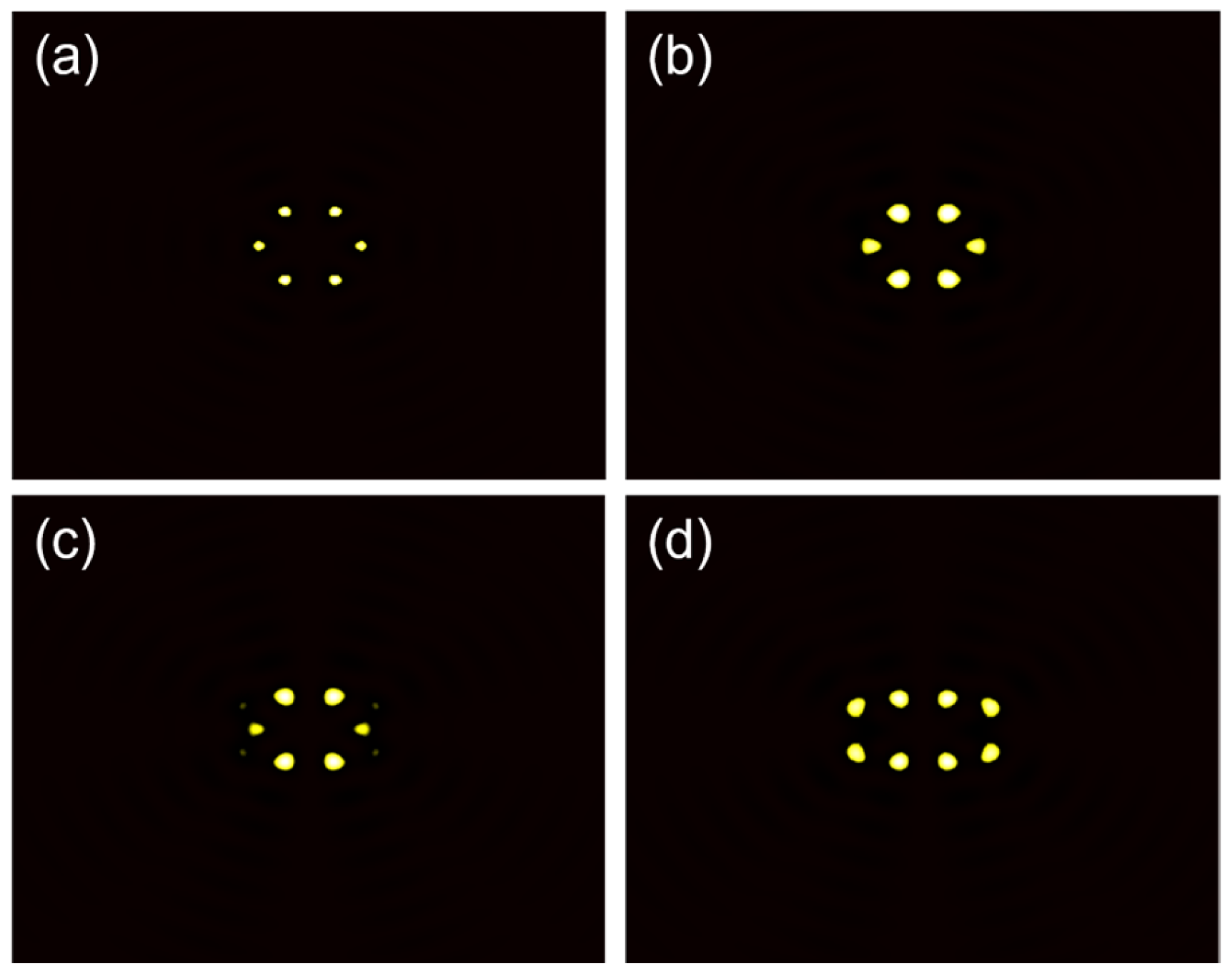
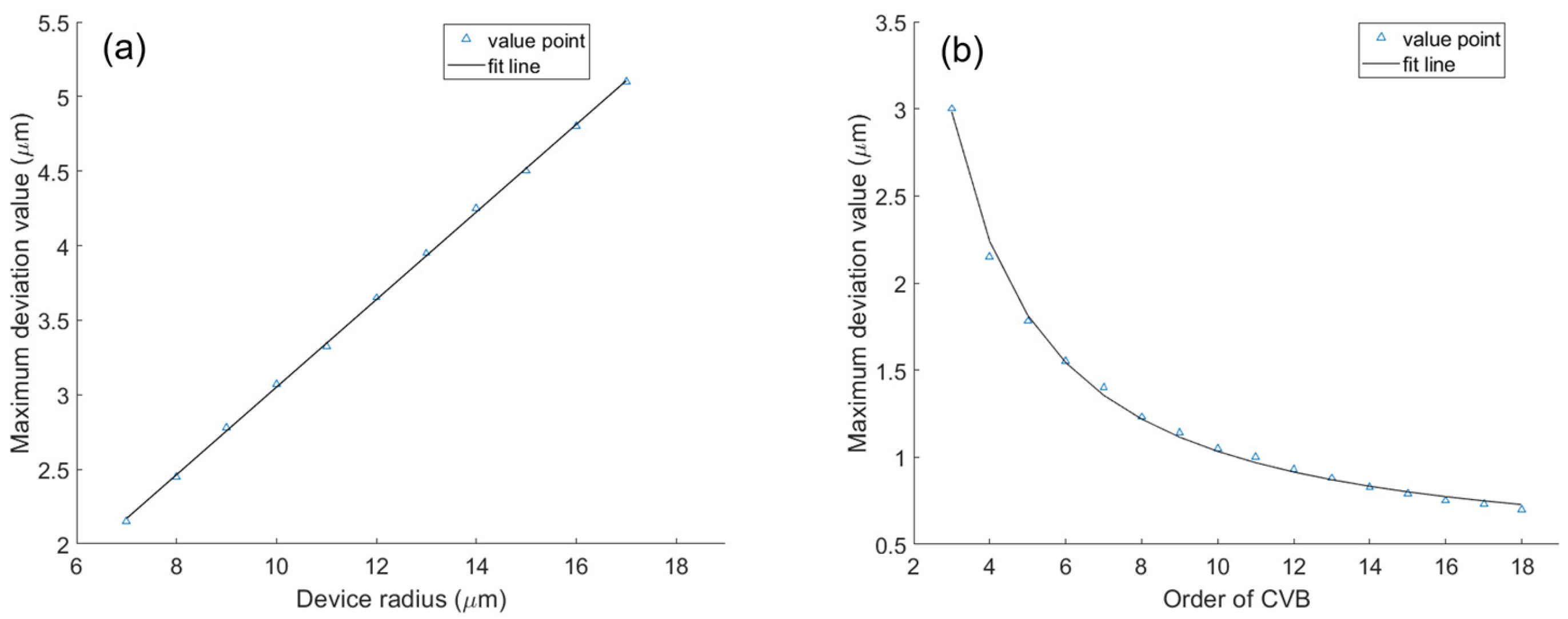
We chose a threshold value for filtering 90% of the maximum intensity to better identify the related focal points. The field distributions after filtering for different offset values are shown in Figure 4. As a result of the filtering process, we eliminated redundant information from the graph and retained only the key areas of high intensity. The number of identified focal points in Figure 4a–c is six, which indicates that they do not reach the deviation limit. However, when the offset is increased to 3   μ m , we can clearly observe additional focal points. This threshold coincides with the emergence of new focuses in the outer layer of the ring pattern. Beyond the critical deviation value, it becomes challenging to identify the accurate related parameters, such as the number of focuses, solely through visual inspection or even with the aid of extra AI-based image recognition algorithms. Moreover, the pattern loses its effectiveness as a reliable indicator of the incidence. Since the modulation of the focusing pattern is characterized by m e r , for a larger device with radius r > r , to maintain an identical focusing pattern, a proportionally larger deviation e is required. This implies a linear relationship between the e and r . Consequently, a larger radius of the annular ring allows for greater tolerance to deviation, enhancing the robustness of the focusing pattern against alignment imperfections. The deviation tolerance for different ring radii is shown in Figure 5a, validating the linear relationship. This phenomenon arises from the increased interaction area between the CVB and the nanostructure, facilitating effective SPP coupling and excitation, thus allowing for greater deviation.
Likewise, we also investigated the influence of the order of the incident beam m . Unlike the relationship observed with the radius, we obtained an inversely proportional relationship between the deviation tolerance and CVB order, as shown in Figure 5b, which stems from the high sensitivity of high-order CVBs to deviations from the center. A higher-order beam possesses a more intricate polarization distribution, making its interaction with the nanostructure more susceptible to disruptions caused by deviation. As m increases, the delicate balance of plasmonic mode excitation required for the formation of the distinct focusing pattern becomes more unstable, leading to a reduced tolerance.

4. Conclusions

In conclusion, we have investigated the interplay between high-order cylindrical vector beams and metallic nanostructures, elucidating the dependence of plasmonic focusing patterns on the incident beam parameters. Our exploration has led to the development of an accurate mathematical model based on Bessel solutions, which reveals the hidden mechanisms behind the focusing patterns. The plasmonic fields exhibit good robustness against the deviations of the incident beam, enabling their potential use for the detection and characterization of high-order CVB. Our finding not only contributes to a deeper understanding of plasmonic nanostructure under high-order CVB interaction but also paves the way for practical applications for novel optical manipulation methods, on-chip photonic devices, and related nanophotonics fields.

Author Contributions

Conceptualization, X.L. and Q.Z.; methodology, X.L. and J.Z.; writing—original draft preparation, H.W.; writing—review and editing, X.L.; supervision, X.L. and Q.Z.; All authors have read and agreed to the published version of the manuscript.

Funding

This research was funded by the National Natural Science Foundation of China (92050202, 12204309, 12304367); the Shanghai Rising-Star Program (22YF1415200, 23YF1415800); and the Open Research Fund of State Key Laboratory of Materials for Integrated Circuits (No. SKL2022).

Institutional Review Board Statement

Not applicable.

Informed Consent Statement

Not applicable.

Data Availability Statement

The original contributions presented in the study are included in the article, further inquiries can be directed to the corresponding authors.

Conflicts of Interest

The authors declare no conflicts of interest.

References

  1. Bhandari, R. Polarization of Light and Topological Phases. Phys. Rep. 1997, 281, 1–64. [Google Scholar] [CrossRef]
  2. Stenholm, S. The Semiclassical Theory of Laser Cooling. Rev. Mod. Phys. 1986, 58, 699–739. [Google Scholar] [CrossRef]
  3. Rubinsztein-Dunlop, H.; Forbes, A.; Berry, M.V.; Dennis, M.R.; Andrews, D.L.; Mansuripur, M.; Denz, C.; Alpmann, C.; Banzer, P.; Bauer, T.; et al. Roadmap on Structured Light. J. Opt. 2016, 19, 013001. [Google Scholar] [CrossRef]
  4. Rashid, M.; Maragò, O.M.; Jones, P.H. Focusing of High Order Cylindrical Vector Beams. J. Opt. A Pure Appl. Opt. 2009, 11, 065204. [Google Scholar] [CrossRef]
  5. Khonina, S.N.; Karpeev, S.V.; Alferov, S.V.; Soifer, V.A. Generation of Cylindrical Vector Beams of High Orders Using Uniaxial Crystals. J. Opt. 2015, 17, 065001. [Google Scholar] [CrossRef]
  6. Zhan, Q. Cylindrical Vector Beams: From Mathematical Concepts to Applications. Adv. Opt. Photon. 2009, 1, 1–57. [Google Scholar] [CrossRef]
  7. Chandrasekaran, R.; Prabakaran, K.; Rajesh, K.B.; Ravi, V. Tight Focusing Properties of Cylindrically Polarized Annular Multi-Gaussian Beam. Optik 2016, 127, 7537–7542. [Google Scholar] [CrossRef]
  8. Chen, S.; Zhou, X.; Liu, Y.; Ling, X.; Luo, H.; Wen, S. Generation of arbitrary cylindrical vector beams on the higher order Poincaré sphere. Opt. Lett. 2014, 39, 5274–5276. [Google Scholar] [CrossRef] [PubMed]
  9. Youngworth, K.S.; Brown, T.G. Focusing of High Numerical Aperture Cylindrical-Vector Beams. Opt. Express 2000, 7, 77–87. [Google Scholar] [CrossRef]
  10. Xiaoqiang, Z.; Ruishan, C.; Anting, W. Focusing Properties of Cylindrical Vector Vortex Beams. Opt. Commun. 2018, 414, 10–15. [Google Scholar] [CrossRef]
  11. Bliokh, K.Y.; Rodríguez-Fortuño, F.J.; Nori, F.; Zayats, A.V. Spin–Orbit Interactions of Light. Nat. Photonics 2015, 9, 796–808. [Google Scholar] [CrossRef]
  12. Šlevas, P.; Orlov, S. Creating an Array of Parallel Vortical Optical Needles. Photonics 2024, 11, 203. [Google Scholar] [CrossRef]
  13. Du, L.; Yang, A.; Zayats, A.V.; Yuan, X. Deep-Subwavelength Features of Photonic Skyrmions in a Confined Electromagnetic Field with Orbital Angular Momentum. Nat. Phys. 2019, 15, 650–654. [Google Scholar] [CrossRef]
  14. Lei, X.; Yang, A.; Shi, P.; Xie, Z.; Du, L.; Zayats, A.V.; Yuan, X. Photonic Spin Lattices: Symmetry Constraints for Skyrmion and Meron Topologies. Phys. Rev. Lett. 2021, 127, 237403. [Google Scholar] [CrossRef] [PubMed]
  15. Lei, X.; Zhan, Q. Topological Charge Constrained Photonic Skyrmion Defects in Split Plasmonic Vortices. ACS Photonics 2023, 10, 3551–3557. [Google Scholar] [CrossRef]
  16. Droop, R.; Ehrmanntraut, D.; Denz, C. Transverse energy flow in an optical Skyrmionic Hopfion. Opt. Express 2023, 31, 11185–11191. [Google Scholar] [CrossRef] [PubMed]
  17. Shi, P.; Du, L.; Yuan, X. Spin photonics: From transverse spin to photonic skyrmions. Nanophotonics 2021, 10, 3927–3943. [Google Scholar] [CrossRef]
  18. Kozawa, Y.; Sato, S. Optical trapping of micrometer-sized dielectric particles by cylindrical vector beams. Opt. Express 2010, 18, 10828–10833. [Google Scholar] [CrossRef] [PubMed]
  19. Ye, H.; Wan, C.; Huang, K.; Han, T.; Teng, J.; Ping, Y.S.; Qiu, C.-W. Creation of Vectorial Bottle-Hollow Beam Using Radially or Azimuthally Polarized Light. Opt. Lett. 2014, 39, 630–633. [Google Scholar] [CrossRef]
  20. Moradi, H.; Shahabadi, V.; Madadi, E.; Karimi, E.; Hajizadeh, F. Efficient Optical Trapping with Cylindrical Vector Beams. Opt. Express 2019, 27, 7266–7276. [Google Scholar] [CrossRef]
  21. Donato, M.G.; Vasi, S.; Sayed, R.; Jones, P.H.; Bonaccorso, F.; Ferrari, A.C.; Gucciardi, P.G.; Maragò, O.M. Optical Trapping of Nanotubes with Cylindrical Vector Beams. Opt. Lett. 2012, 37, 3381–3383. [Google Scholar] [CrossRef] [PubMed]
  22. Van, M.; Ushakova, K.; Bastiaansen, C.; Pereira, S.; Urbach, H.; Broer, D. Enhanced Lithographic Resolution Using Longitudinal Polarization State of Light. J. Micro/Nanolithography MEMS MOEMS 2015, 14, 043509. [Google Scholar] [CrossRef]
  23. Helseth, L.E. Roles of Polarization, Phase and Amplitude in Solid Immersion Lens Systems. Opt. Commun. 2001, 191, 161–172. [Google Scholar] [CrossRef]
  24. Li, X.; Cao, Y.; Gu, M. Superresolution-Focal-Volume Induced 3.0 Tbytes/Disk Capacity by Focusing a Radially Polarized Beam. Opt. Lett. 2011, 36, 2510–2512. [Google Scholar] [CrossRef] [PubMed]
  25. Lou, K.; Qian, S.-X.; Wang, X.-L.; Li, Y.; Gu, B.; Tu, C.; Wang, H.-T. Two-Dimensional Microstructures Induced by Femtosecond Vector Light Fields on Silicon. Opt. Express 2012, 20, 120–127. [Google Scholar] [CrossRef] [PubMed]
  26. Shi, C.; Guo, L.; Cheng, M.; Li, R. Scattering of a High-Order Vector Bessel Gaussian Beam by a Spherical Marine Aerosol. J. Quant. Spectrosc. Radiat. Transf. 2021, 265, 107552. [Google Scholar] [CrossRef]
  27. Tian, H.W.; Jiang, W.X.; Li, X.; Zhang, X.G.; Yang, Z.Y.; Cui, T.J. Generation of High-Order Orbital Angular Momentum Beams and Split Beams Simultaneously by Employing Anisotropic Coding Metasurfaces. J. Opt. 2019, 21, 065103. [Google Scholar] [CrossRef]
  28. Sancho-Parramon, J.; Bosch, S. Dark Modes and Fano Resonances in Plasmonic Clusters Excited by Cylindrical Vector Beams. ACS Nano 2012, 6, 8415–8423. [Google Scholar] [CrossRef] [PubMed]
  29. Xiao, F.; Shang, W.; Zhu, W.; Han, L.; Premaratne, M.; Mei, T.; Zhao, J. Cylindrical Vector Beam-Excited Frequency-Tunable Second Harmonic Generation in a Plasmonic Octamer. Photonics Res. 2018, 6, 157–161. [Google Scholar] [CrossRef]
  30. Das, T.; Schuller, J.A. Dark Modes and Field Enhancements in Dielectric Dimers Illuminated by Cylindrical Vector Beams. Phys. Rev. B 2017, 95, 201111. [Google Scholar] [CrossRef]
  31. Feng, F.; Si, G.; Min, C.; Yuan, X.; Somekh, M. On-Chip Plasmonic Spin-Hall Nanograting for Simultaneously Detecting Phase and Polarization Singularities. Light Sci. Appl. 2020, 9, 95. [Google Scholar] [CrossRef] [PubMed]
  32. Mei, S.; Huang, K.; Liu, H.; Qin, F.; Mehmood, M.Q.; Xu, Z.; Hong, M.; Zhang, D.; Teng, J.; Danner, A.; et al. On-Chip Discrimination of Orbital Angular Momentum of Light with Plasmonic Nanoslits. Nanoscale 2016, 8, 2227–2233. [Google Scholar] [CrossRef] [PubMed]
  33. Chen, W.; Abeysinghe, D.C.; Nelson, R.L.; Zhan, Q. Plasmonic Lens Made of Multiple Concentric Metallic Rings under Radially Polarized Illumination. Nano Lett. 2009, 9, 4320–4325. [Google Scholar] [CrossRef] [PubMed]
  34. Liu, Z.; Steele, J.M.; Srituravanich, W.; Pikus, Y.; Sun, C.; Zhang, X. Focusing Surface Plasmons with a Plasmonic Lens. Nano Lett. 2005, 5, 1726–1729. [Google Scholar] [CrossRef]
  35. Lei, X.; Ren, Y.; Lu, Y.; Wang, P. Lens for Efficient Focusing of Bloch Surface Waves. Phys. Rev. Appl. 2018, 10, 044032. [Google Scholar] [CrossRef]
  36. Fu, Y.; Wang, Y.; Zhang, Y.; He, Y.; Min, C.; Yuan, X. Detecting Cylindrical Vector Beams with an On-Chip Plasmonic Spin-Hall Metalens. Opt. Express 2022, 30, 10758–10769. [Google Scholar] [CrossRef] [PubMed]
  37. Zhang, C.; Min, C.; Zhang, Y.; Fu, Y.; Li, L.; Wang, Y.; Yuan, X. Detection of Cylindrical Vector Beams with Chiral Plasmonic Lens. Chin. Opt. Lett. 2022, 20, 023602. [Google Scholar] [CrossRef]
  38. Qin, Y.; Li, Y.; Deng, D.; Liu, Y.; Sun, M. Ultracompact Biosensor Based on a Metalens with a Longitudinally Structured Vector Beam. Appl. Opt. 2019, 58, 4438–4442. [Google Scholar] [CrossRef] [PubMed]
  39. Wang, R.; Zhang, C.; Yang, Y.; Zhu, S.; Yuan, X.-C. Focused Cylindrical Vector Beam Assisted Microscopic pSPR Biosensor with an Ultra Wide Dynamic Range. Opt. Lett. 2012, 37, 2091–2093. [Google Scholar] [CrossRef]
  40. Liu, H.; Li, H.; Zheng, Y.; Chen, X. Nonlinear Frequency Conversion and Manipulation of Vector Beams. Opt. Lett. 2018, 43, 5981–5984. [Google Scholar] [CrossRef]
  41. Milione, G.; Nguyen, T.A.; Leach, J.; Nolan, D.A.; Alfano, R.R. Using the Nonseparability of Vector Beams to Encode Information for Optical Communication. Opt. Lett. 2015, 40, 4887–4890. [Google Scholar] [CrossRef] [PubMed]
  42. Montagnac, M.; Brûlé, Y.; Cuche, A.; Poumirol, J.-M.; Weber, S.J.; Müller, J.; Larrieu, G.; Larrey, V.; Fournel, F.; Boisron, O.; et al. Control of Light Emission of Quantum Emitters Coupled to Silicon Nanoantenna Using Cylindrical Vector Beams. Light Sci. Appl. 2023, 12, 239. [Google Scholar] [CrossRef] [PubMed]
  43. Ndagano, B.; Nape, I.; Cox, M.A.; Rosales-Guzman, C.; Forbes, A. Creation and Detection of Vector Vortex Modes for Classical and Quantum Communication. J. Light. Technol. 2018, 36, 292–301. [Google Scholar] [CrossRef]
  44. Bravo-Abad, J.; Martín-Moreno, L.; García-Vidal, F.J. Transmission Properties of a Single Metallic Slit: From the Subwavelength Regime to the Geometrical-Optics Limit. Phys. Rev. E 2004, 69, 026601. [Google Scholar] [CrossRef] [PubMed]
  45. Lindberg, J.; Lindfors, K.; Setälä, T.; Kaivola, M.; Friberg, A. Spectral Analysis of Resonant Transmission of Light through a Single Sub-Wavelength Slit. Opt. Express 2004, 12, 623–632. [Google Scholar] [CrossRef] [PubMed]
  46. Ebbesen, T.W.; Lezec, H.J.; Ghaemi, H.F.; Thio, T.; Wolff, P.A. Extraordinary Optical Transmission through Sub-Wavelength Hole Arrays. Nature 1998, 391, 667–669. [Google Scholar] [CrossRef]
  47. Yang, S.; Chen, W.; Nelson, R.L.; Zhan, Q. Miniature Circular Polarization Analyzer with Spiral Plasmonic Lens. Opt. Lett. 2009, 34, 3047–3049. [Google Scholar] [CrossRef]
  48. Novotny, L.; Hecht, B. Principles of Nano-Optics, 2nd ed.; Cambridge University Press: Cambridge, UK, 2012; ISBN 978-1-107-00546-4. [Google Scholar]
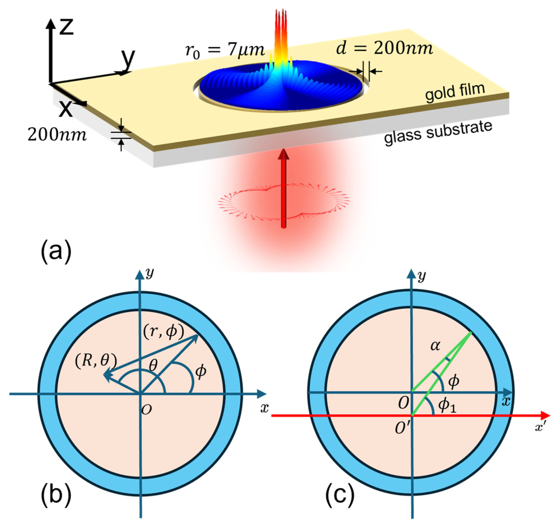
Figure 1. (a): Schematic diagram of the plasmonic focusing pattern with the interaction between CVBs and metallic nanoring structure. (b,c): Geometric layout of metallic ring structure with parameters and coordinates under (b) ideal alignment condition and (c) deviation condition; the blue regime represents the nanoring.
Photonics 11 00579 g001
Figure 2. Simulation results of normalized intensity distributions of plasmonic field with interactions between CVB and annular ring. (ac): Orders of CVB for 1, 2, and 5 as the center are aligned with the center of the annular ring. The scale bar represents a distance of 1   μ m . The plasmonic fields range from −2.5 to 2.5 μ m for both x and y directions in (ac).
Photonics 11 00579 g002
Figure 3. The dependence of the field distribution on the deviation distance between the centers of the annular ring and CVB with an order of 4 for (a) e = 0 ; (b) e = 0.5   μ m ; (c) e = 1   μ m ; (d) e = 2   μ m ; (e) e = 3   μ m ; and (f) e = 4   μ m . The insets in (b,c) represent the theoretical results calculated by Equation (8), as the deviation is not comparable to r . The scale bar represents a distance of 1   μ m . The plasmonic fields range from −2.5 to 2.5 μ m for both x and y directions in (af).
Photonics 11 00579 g003
Figure 4. The field distributions of incident CVB with order 4 under 90% of the maximum intensity scale filtration for different offset values (a) e = 1   μ m ; (b) e = 2   μ m ; (c) e = 2.15   μ m (critical deviation value); and (d) e = 3   μ m .
Photonics 11 00579 g004
Figure 5. The maximum deviation value as a function of (a) device radius and (b) order of CVB. The colored lines in the figures give the corresponding approximation-fit lines. The order of CVB is fixed as 4 in (a) and the radius of ring is fixed as 7   μ m in (b).
Photonics 11 00579 g005
Disclaimer/Publisher’s Note: The statements, opinions and data contained in all publications are solely those of the individual author(s) and contributor(s) and not of MDPI and/or the editor(s). MDPI and/or the editor(s) disclaim responsibility for any injury to people or property resulting from any ideas, methods, instructions or products referred to in the content.