1. Introduction
Surface plasmon polaritons (SPPs) on a metal surface are collective oscillations of free electrons with photons that produce an electromagnetic spectrum, which transpire as they migrate along the metal–dielectric junction [
1]. The travel of the SPPs is in a direction paralleling the metal surface, and it is in the direction perpendicular to the metal surface that their electric field strength decays exponentially; thus, SPPs are bound to the metal surface and exhibit surface-localized properties [
2,
3]. When the incident light and the free electrons on the metal surface have the same frequency, the electromagnetic field energy can be well localized on the metal surface, which enhances the cooperation between transmitted light and other substances. Therefore, by utilizing this special optical property, a new path can be opened for the design of novel optical sensors, whose theory and related techniques have become a research field at the forefront of nanophotonics, with a widespread application in ultra-diffractive lithography, beamsplitters [
4,
5], spatial technology, optical switches [
6], sensors [
7], and highly integrated photonic circuits, among others.
SPPs in nano-optoelectronic devices have attracted the interest of many researchers by virtue of their great advantages over conventional electronic devices, leading to the design of a wide variety of waveguide structures, such as filters [
8,
9,
10], rectangular waveguides based on MIM [
11,
12], nanoshells [
13], nanowires [
14,
15], and farnesoidal resonances [
16,
17,
18,
19], among others. Among the various structures mentioned above, MIM waveguides have been recognized by researchers as having advantages such as a simple structure, easy processing and acceptable propagation length, and have been designed into various types of micronano-optoelectronic devices. One of the unique phenomena based on the MIM waveguide using the coupled cavity resonance, Fano resonance has aroused the interest of researchers from various countries because the Fano resonance phenomenon produces steep and sharp resonance transmission spectral lines, which are affected by much less compared to other micro-nano photonic devices. However, in the MIM waveguide structure, its structural composition dictates the existence of a slit, which ensures that SPPs can propagate efficiently in this slit, even in the subwavelength state. In this paper, the surface plasmon MIM waveguide is used as the sensing structure, and the Fano resonance effect is used as the sensing basis.
Fano resonance has been labeled as a phenomenon that produces a dispersive resonance with an unsymmetrical line formed by the integration of two scattering amplitudes, one for scattering in the continuous state (background-dependent) while the other is for excitation in the dispersive state (resonance-dependent). In close proximity to the resonance energy, the change in the amplitude of the backscattering with energy is usually gentle; however, the amplitude of the resonance scattering, both in magnitude and in phase, changes quite rapidly, leading to the onset of asymmetry [
20,
21]. The output waveform of the Fano resonance is extremely susceptible to fluctuation in the surrounding environment, and small changes in the environment can cause large wavelength drifts [
22,
23,
24]. Therefore, the Fano resonance-based MIM waveguide metal structure can be applied to the sensing field to greatly improve the sensitivity and provide a better choice for high-precision measurements. Such sensors have now moved from the early stages of proof-of-concept demonstration and theoretical modeling to further device and system development and practical applications. Research efforts are increasingly focused on the detection of samples from more realistic and complex media. One such area is the development of portable rapid diagnostic devices for immediate care. Another important area is vapor detection [
25].
Rakhshani et al., in 2018, designed a plasma nanosensor consisting of an array of nanorods inside a square resonant cavity coupled with two slot cavities. Their sensor properties were obtained by filling with a grape solution and varying its concentration, with a sensitivity of 892 nm/RIU [
26]. Chen Ying et al., in 2019, devised a compact optical waveguide structure with a MIM waveguide coupled to a metal baffle SCRR, and their structure also obtained desirable sensing characteristics, in which the sensitivity was as high as 1120 nm/RIU [
27]. A. Noual et al. proposed resonators consisting of a bus waveguide made of graphene coupled to resonators inserted along the waveguide, where each resonator consisted of a set of two coupled graphene nanoribbons (CGNR) [
28]. Yamina Rezzouk et al. proposed a sensor connected to an infinite waveguide in a T-shaped cavity consisting of a short segment of length d
0 and two side branches of length d
1 and d
2. The whole system consists of a MIM plasmonic waveguide that operates in the telecommunication range with a sensitivity of 1400 nm/RIU [
29]. The performance of the sensors presented herein is superior to the performance of the sensors presented in the literature [
30,
31,
32]. And compared to the sensors proposed in the literature [
33], although the sensitivity of the sensors proposed herein is slightly lower, the sensors proposed herein, however, can be adjusted with multiple geometrical parameters to suit different applications.
The structure of this new nanoscale refractive index sensor, designed in this paper, consists of a MIM waveguide with two rectangular baffles and a ring with a rectangular annular cavity, which is simple and easy to parameterize. Changing the geometrical parameters of the structure affects both the transmittance and the position of the Fano resonance peaks, and the sensor structure has a large number of adjustable geometrical parameters. In this paper, when the sensor was used to detect the concentrations of electrolyte sodium and potassium ions in human blood, it was found that the structure was sensitive to changes in the refractive index and was able to achieve sensitivities of 0.495 nm/mgdL−1 and 0.6375 nm/mgdL−1. The structure has excellent sensing properties and can be used for concentration detection in solutions as well as for sensors at the nanoscale.
In this paper, based on existing studies and basic theories, a nanoscale sensor with a simple structure is proposed and investigated, which is derived from the coupling of a MIM and CRERR structure. Using COMSOL 5.4 software and in conjunction with the finite element method (FEM) [
34], we have carried out an in-depth simulation study of the sensing characteristics of the designed sensor. This paper addresses the influence of various geometric parameters on the transmission characteristics, which include the exterior radius of the ring, the length of the baffle rectangle, the rotation angle of the external rectangular ring, the height of the outer rectangular ring, as well as the coupling distance among MIM waveguides in relation to the CRERR structure.
2. Structure and Methods
Given that the 2D model is more simplified than the 3D model, and the 2D model can reduce computational complexity while retaining key physical properties, it makes the study more efficient. Secondly, the height of the proposed structure is much larger than the skinning depth of the SPPs, so that the 2D model can be used instead of the 3D model for simple calculations. As shown in
Figure 1, the entire sensor structure is symmetric along the centerline and comprises a MIM waveguide having a rectangular baffle coupled to a CRERR structure. The radius of the outside circle and the radius of the inside circle of the CRERR structure are denoted by R and r, respectively, and the values of R and r satisfy R = r + 50 nm. In addition to the above-mentioned parameters, the height of the rectangular stopper is precisely set to h, and g is the key value used to describe the doubling distance of the coupling between the MIM waveguide and the CRERR. Furthermore, α indicates the specific angle at which the rectangular annular cavity is rotated around the center of its torus, while L represents, in turn, the height of the rectangular annular cavity. Additionally, w serves as a common parameter that defines not only the width of the MIM waveguide but also the width of the annular cavity, the rectangular cavity and the rectangular baffle. When the value of w is in a small range, the SPPs in the up-and-down metal–dielectric interfaces will exhibit two dispersion modes due to mutual coupling. In the even-symmetric mode, the SPPs can maintain a long propagation distance and have a relatively low energy loss. In order to achieve efficient energy transmission and low loss in this study, we deliberately designed all the structures based on the even-symmetric mode. To achieve this, the width w is precisely set to 50 nm in the MIM waveguide structures to ensure that only one transmission mode, the even-symmetric mode, exists.
In order to have a better excitation of SPPs and because silver has a stronger electric force as well as less powerful consumption, metallic silver was used for the metal layer in this study. In
Figure 1, the yellow area is for silver material, while the white area is for air, whose dielectric constant is 1. The dispersion model used in this paper to represent the dielectric constant of metallic silver uses the Debye–Drude dispersion equation as follows [
35]:
where
is the quiescent dielectric constant,
is the relative permittivity at the wireless angular frequency,
is the permittivity in vacuum,
is the relaxation time, and
is the electrical conductivity of silver.
In some special cases, such as on the surface of nanostructures or in waveguide structures with specific designs, the TE-polarized modes may be converted into TM-polarized modes through certain mechanisms (e.g., mode conversion or scattering), and thus, SPPs may be generated, which needs to be achieved by precisely designing the geometrical parameters and material properties of nanostructures. Therefore, in general, TE polarization modes do not directly generate SPPs, and TE polarization modes in nanostructures can generate SPPs under specific conditions [
36]. Electromagnetic waves can excite SPPs only in the TM mode on the layer surface of the metal. Hence, this paper focuses on analyzing the TM mode, and its equation in the MIM waveguide can be described as [
37]
where
represents the waveguide width, and
is the wavevector in the waveguide,
,
. The wavevector
in a vacuum is denoted as
;
is determined by Equation (2), and
and
denote the dielectric constants in the metal and dielectric.
Given the high cost of nanoscale device fabrication, simulation has emerged as an efficient means of allowing us the flexibility to adapt the structure of the sensor and ultimately maximize its performance. In this paper, COMSOL 5.4 software was used to successfully fabricate a 2D model structure of CRERR and subsequently perform an exhaustive simulation analysis. The overall simple simulation is described as follows: (1) Identify the appropriate physical field modules and interfaces. (2) The geometric drawing tool that comes with COMSOL 5.4 can be used to draw the design structure. (3) Before performing the simulation, the port locations of the model, the applicable material model and the corresponding fluctuation formulae first need to be carefully selected and configured. Subsequently, in order to ensure the accuracy and efficiency of the simulation, the entire simulation area will be meshed using a triangular meshing method. (4) Parametric scanning can be easily set up in COMSOL’s simulation environment using its own solver. Specifically, specify a wavelength range from 1600 nm to 3000 nm, and set the step size to 1 nm. Once these settings are made, simply click the ‘Calculate’ button, and COMSOL will automatically perform a parametric scan to compute and simulate the response of the physical model point by point in this wavelength range.
In refractive index sensors, sensitivity (
) is generally defined as the amount of variation in the value of the resonance pole position experienced when there is a unit movement in the refractive index. This concept can be precisely expressed by the following mathematical formula: [
38,
39]:
where
is the modification of the refractive index, and
is the change in resonance wavelength. The unit of
can be expressed as nm/RIU.
The FOM is a reflection of the holistic performance of the refractive index sensor and is another key parameter for measuring many sensors, which can be expressed by the formula
where
denotes the half-height width.
3. Results and Analysis
In the preliminary study of this paper, we compared the performance of a single annular cavity structure with that of a CRERR structure sensor. Through careful comparative analyses, we found that the CRERR structure sensor demonstrated slightly higher sensitivity over a preset range of refractive index fluctuations, and its FOM value was superior. In view of these advantages, we decided to further investigate the properties and potential of the CRERR structure’s sensor in depth. The initial parameters of the structure are as follows: R = 250 nm, g = 10 nm, h = 160 nm, α = 0° and L = 60 nm.
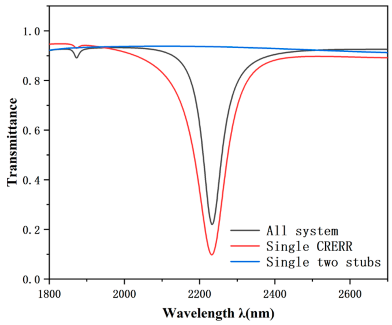
A series of exhaustive simulation analyses have been carried out in order to thoroughly investigate the formation mechanism of the Fano resonance and its spreading properties in the sensor. These analyses cover the overall structure of the system, the stand-alone CRERR structure, and the simplified double baffle composition. As shown in
Figure 2, we can see and understand the complete system fabric that the transmittal frequency profile exhibits as an unsymmetrical sharp form, deriving its linear shape from the interference of two scattering amplitudes—one in the continuous state (associated with the background) and the other in the discrete state of excitation (associated with the resonance). The energy of the resonant state must be in the energy range of the continuous state (i.e., the background) for this effect to occur. In the vicinity of the resonance energy, the amplitude of the background scattering usually varies gently with energy; however, the amplitude of the resonance scattering, both in magnitude and in phase, varies quite rapidly, leading to the onset of asymmetry. In the structure containing only two baffles, the transmission spectral line presents an approximately straight line feature, and all points on this line possess high transmittance. However, when we introduced the CRERR structure into the system, the collection capability of the entire system for electric fields and the capture capability of SPPs were significantly improved. This improvement makes the system more advantageous for sensor performance evaluation.
In an attempt to explain the generation process of the Fano resonance in more detail, we further investigated the distributed magnetic field at the resonance inclination (
,
) for a single CRERR structure and the whole system, as depicted in
Figure 3. It is noteworthy from the figure, that here, the SPPs could pass through the waveguide and pair to the CRERR structure in both the individual CRERR structure and the whole system structure. The distributions of the naturalized magnetism are dominated by the CRERR fabric, which is sparsely observed in the bus waveguide, indicating that significant resonance occurs. Moreover, we can also see from the figure that the CRERR’s upper and lower parts are inverted, and the overall structure is similar to the normalized magnetic field distributed by a single CRERR structure, but the addition of the rectangular baffle increases the propagation of the SPPs throughout the system, which further contributes to the formation of the Fano resonance.
We systematically adjusted the values of the refractive indices, which were set to 1.00, 1.01, 1.02, 1.03, 1.04 and 1.05, and carried out an exhaustive comparative study of the same values. From
Figure 4a, it can be seen that the shape of the transmission spectral curve is constant when the refractive index n is varied, and the curve undergoes an almost equidistant redshift when the refractive index n is increased. As illustrated in
Figure 4b, the displacement of the inclination wavelength changes linearity according to the difference in the refractive index n. It is evident that, based on these features, this can be used as a refractive index transducer in our presented structure. After calculating the skewness of the sensitivity fit line, an optimal parameter for the construction was calculated, and the sensitivity of the transducer obtained reached 3180 nm/RIU and a FOM of 54.8, which is the optimal parameter for this structure.
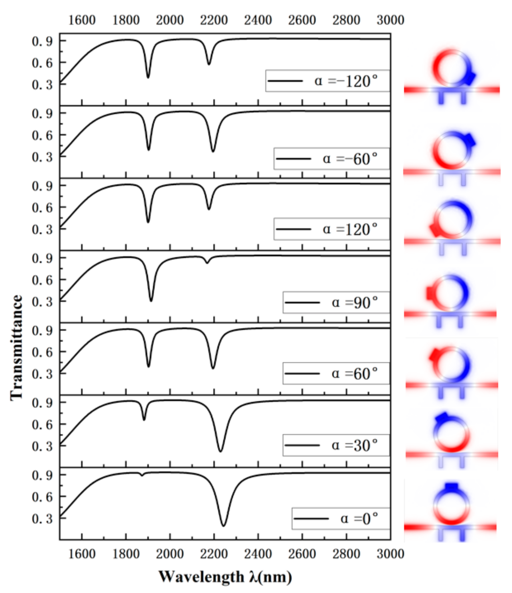
We set the values of α to −120°, −60°, 120°, 90°, 60°, 30° and 0°, and as demonstrated in
Figure 5, the transmission curves, when rotated at the same angle counterclockwise and clockwise, have curves with essentially the same shape, so it is sufficient for us to study the case where α is greater than 0°. As α changes from 0° to 120°, a shift of the curve to the left is observed; i.e., the S of the sensor decreases, and the FOM decreases. After that, we observed the magnetic field distribution in the lumen of CRERR from several perspectives, finding that the differential magnetic scene distribution is different at different angles, and the magnetic scene concentration is higher where the cavity is located, while the magnetic field distribution of these structures is symmetric near the centerline of the rectangular toroidal cavity. This is an indication of the fact that these structures are in the same resonance mode and that the location of the rectangular annular cavity leads to differences in these contrasting structures, with the rectangular annular cavity region being the structure that predominantly binds the energy. When α is 0° the transmission spectrum is an unsymmetrical curve, having an ultra-low transmit rate and a great range of wavelengths, which indicates that this is a Fano resonance of high sensitivity.
The above study shows that the transmission spectral curves of the sensor are basically the same for the same angle of counterclockwise and clockwise rotation, and the performance of the sensor improves as the angle of rotation of the rectangular annular cavity decreases. Thus, the structure when α is 0° is chosen as the main structure to be studied in the following discussion.
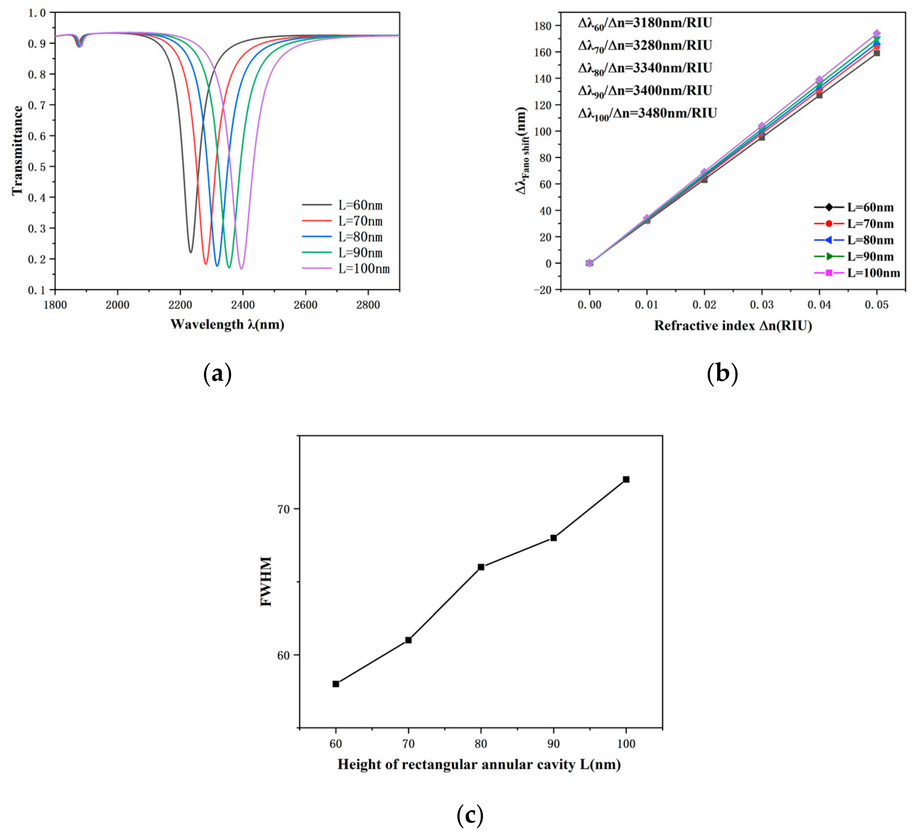
An in-depth study of the rectangular annular cavity was carried out by investigating its height L at 60 nm, 70 nm, 80 nm, 90 nm and 100 nm. As shown in
Figure 6a, the transmission spectrum is red-shifted with increasing L. This is due to the fact that the increase in L causes an extension of the effective length of the structure, which induces a redshift of the resonance trough, but the change in the transmittance is not very significant.
Figure 6b indicates that as the height of the rectangular annular cavity increases, there is no significant effect on the sensitivity change. From
Figure 6c, it is observed that the FWHM becomes dramatically larger as the height L from 60 nm to 100 nm is added, and the FWHM is smallest at a rectangular annular cavity height of 60 nm, and the FWHM is 72 nm at a L of 100 nm. Since the effect on both the transmission spectrum and sensitivity is insignificant when L is varied, it can be concluded that the FOM is maximum when L is 60 nm, which is when the sensor’s performance is best. Therefore, after comprehensive consideration, 60 nm is the most suitable height for the rectangular annular cavity.
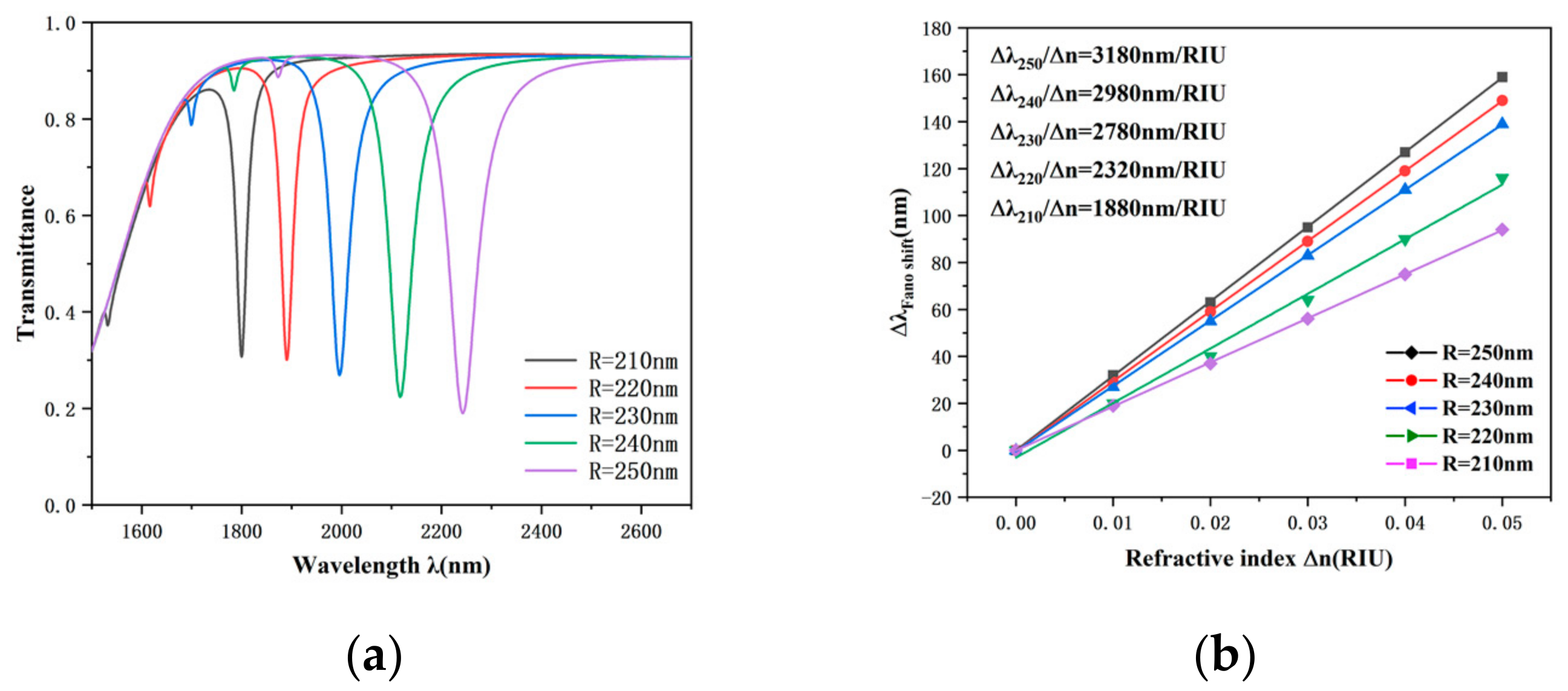
We then estimated the impact of R on the entire system. The parameters of R are adjusted to 210 nm, 220 nm, 230 nm, 240 nm and 250 nm, illustrated in
Figure 7a, which demonstrates that R has the lowest transmittance and maximum wavelength when it is 250 nm. As R increases, the transmission spectral profile shows a significant redshift, which is attributed equally to the expansion of the reactive length of the structure due to the increase in R, which leads to a redshift of the resonance trough. The sensitivity fit line for this structure is provided in
Figure 7b, from which it can be observed that linearity between the varying refractive index and the varying wavelength exhibits an excellent linear relationship. In addition to this, the sensitivity of the CRERR structure is significantly improved as the outer radius R of the structure continues to increase. We also note that the growth of R increases susceptibility from 1880 nm/RIU to 3180 nm/RIU, indicating that the outer radius R is the main geometrical parameter for the structure to enhance sensitivity. In summary, we chose 250 nm as the outer radius of the structure in this paper, at which point the structure has a higher S and FOM sensitivity.
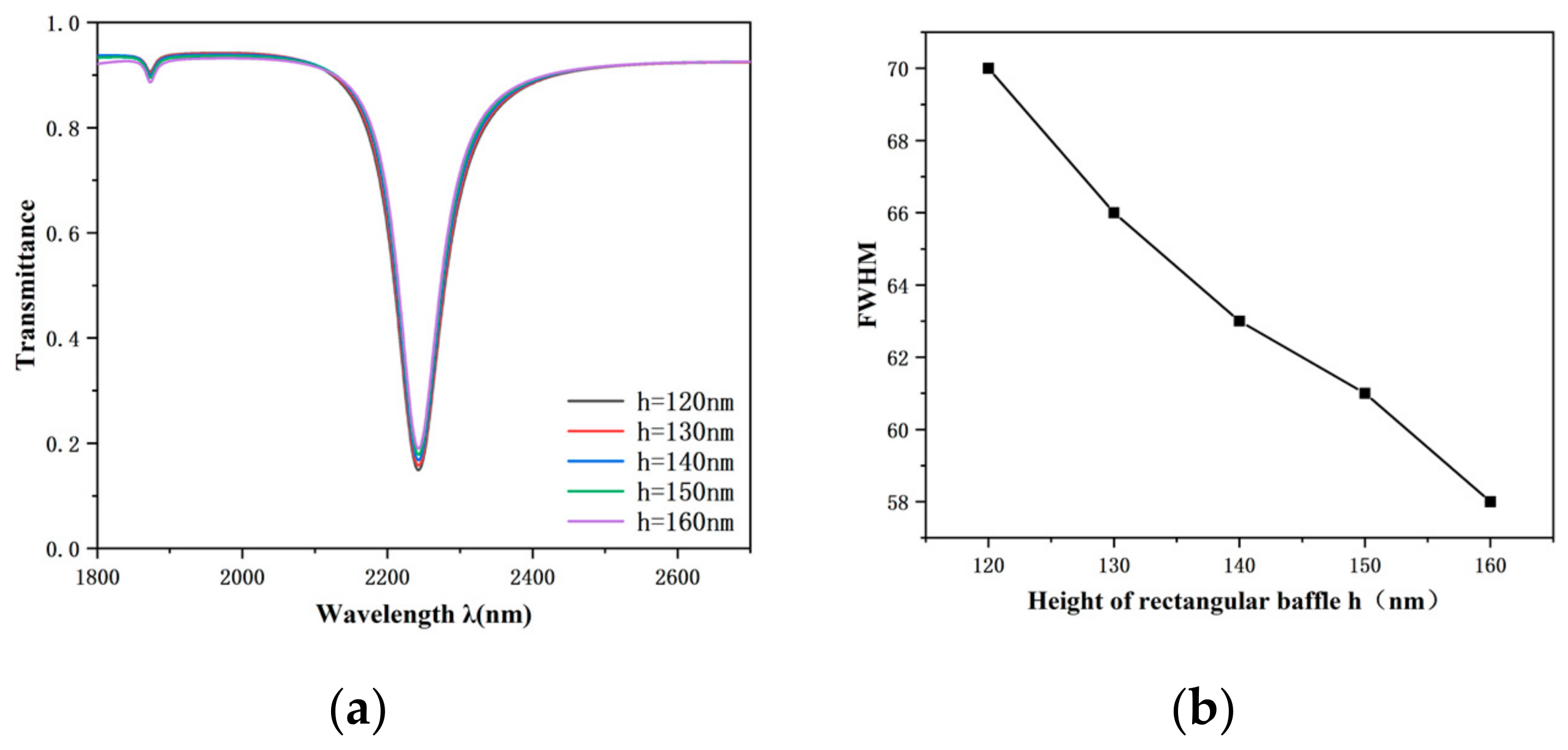
Then, this paper evaluated the impact of the MIM waveguide’s structural parameters on the transmission properties of this sensor. The two rectangular baffle heights h grew from 120 nm to 160 nm, with a step interval of 10 nm for five sets of data. As shown in
Figure 8a, the tilted wavelength and transmittance of the Fano resonance do not significantly change when h is varied, and the degree of asymmetry of the transmission spectral curve does not change significantly. During Fano resonance production, a succession of broad bands is generated by the MIM waveguide. As shown in
Figure 8b, the height of the rectangular baffle also has some effect on the FWHM, and it can be seen from the experiment that as the height h of the rectangular baffle increases, the corresponding FWHM value becomes smaller. The FWHM is minimized at 58 nm when h is 160 nm.
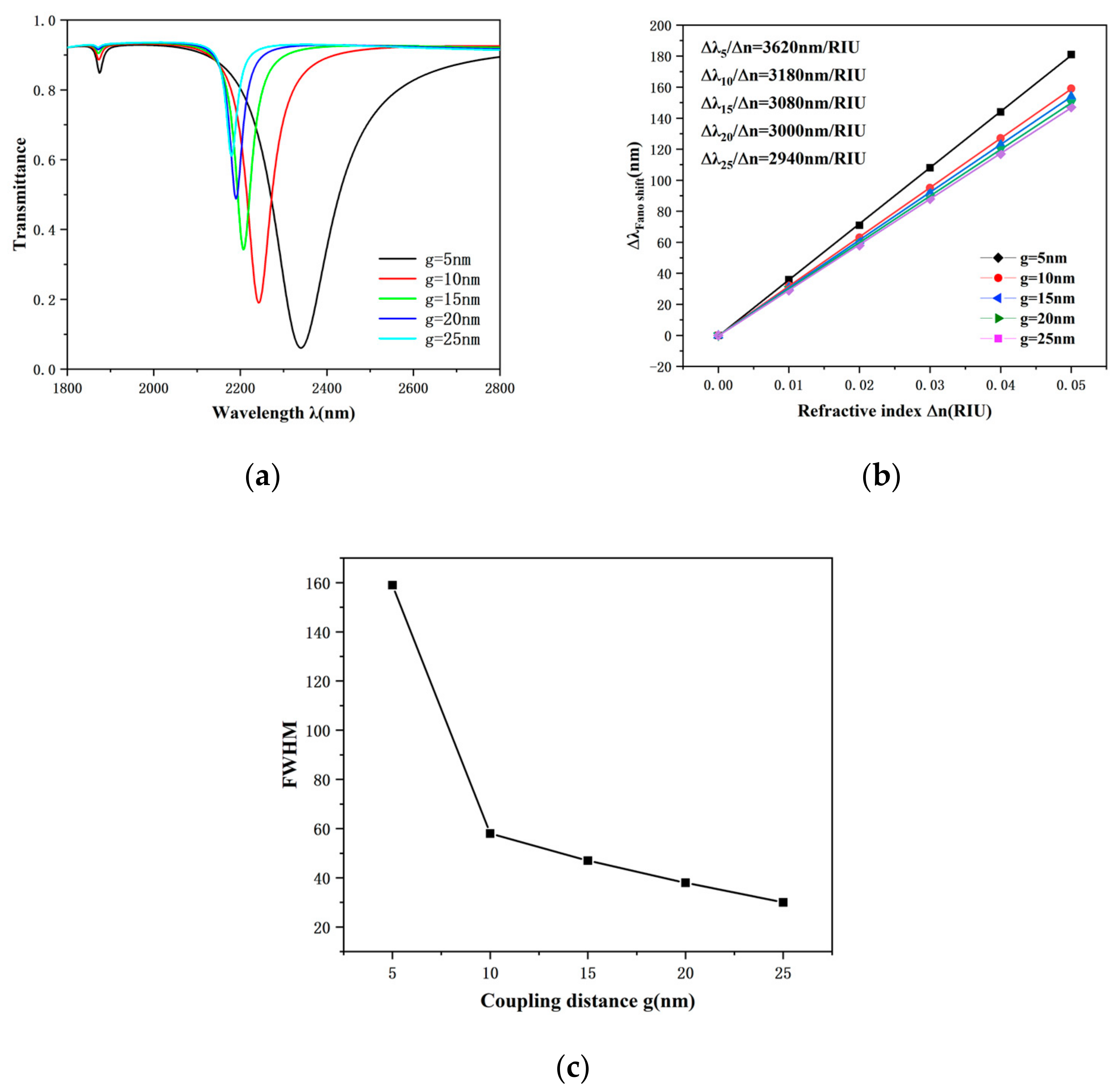
Next, we will deeply exploit the effect of the coupling distance between the waveguide and the CRERR on the transmission features. Specifically, we set the starting value of the coupling distance g to be 5 nm. Take this as a benchmark, and follow the increment of 5 nm up to 25 nm. By observing
Figure 9a, we can distinctly see that the transmission spectral profile significantly shifts towards the short wavelength (i.e., blueshift) with the growth of the coupling distance, and the transmittance also shows an increasing trend. Further,
Figure 9c shows that the FWHM value decreases with an increasing coupling distance, a phenomenon that indicates that, as the coupling gap between the waveguide and the CRERR structure widens, the coupling effect between them becomes weaker, while the electric field strength also weakens accordingly [
40]. Therefore, by the choice of a suitable coupling distance g, a transmission spectrum with a lower transmittance can be obtained. When
, the corresponding FWHM value increases dramatically. As shown in
Figure 9b, the sensitivity decreases as the coupling distance increases but decreases at coupling distances greater than 10 nm. The sensitivity at this point is maximized to 3620 nm/RIU, as g is equal to 5 nm, but the corresponding FWHM value is as high as 159 nm, and the FOM value is only 22.76, as shown in Equation (4). The larger FWHM clearly destroys the FOM of the structure, as the coupling distance is less than 10 nm. After comprehensive consideration, 10 nm was selected as the preferable coupling length for the submitted sensor. At this point, the sensitivity of the proposed sensor is 3180 nm/RIU with a FOM value of 54.8.
4. Biological Sensing Applications
The sensor proposed in this work has a simple structure and high sensitivity; thus, we applied it as a sensor for detecting electrolyte concentrations in human blood. The balance between sodium (
) and potassium (
) ions in electrolytes ensures the functioning of the body’s cells, and the monitoring of
and
concentrations plays an extremely important role in the control of cardiovascular and neurological diseases. The linear relationship between the refractive index and the
concentration and
concentration at constant temperature is expressed as the following [
41]:
where
and
denote the concentration of
and
, respectively, and
and
represent the concentration factors of
and
, respectively, whose values are set to 30 and 50, respectively. Furthermore,
and
are the refractive index values for different concentrations of
and
, respectively. The sensitivity of the sensor for detecting electrolyte concentrations can be expressed as
where
represents the shift in the transmission spectrum, and
represents the change in the concentration of the detected substance.
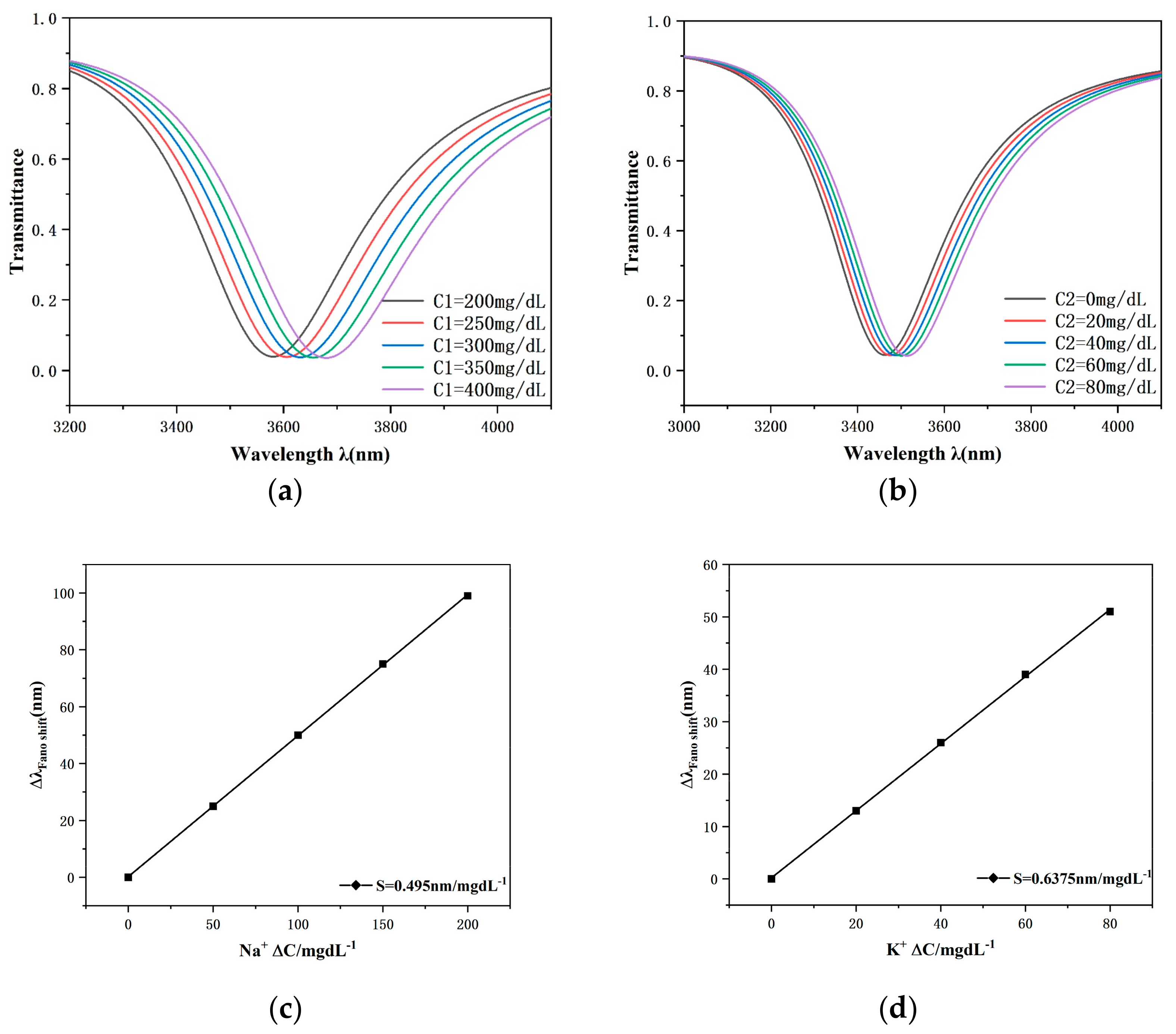
Because of the high optical activity of the surface plasmon excitations in this sensor system, it is theoretically possible to place small amounts of blood samples in the waveguide and resonator. In addition, a change in the concentration of the sample results in a change in the refractive index of the sensor, which indirectly reflects the change in concentration by calculating the shift in the transmission spectrum caused by the change in refractive index. The structural parameters of the proposed sensor were fixed at R = 250 nm, h = 160 nm, α = 0°, L = 60 nm and g = 10 nm; the concentrations of were set to 200, 250, 300, 350 and 400 mgdL−1; and the concentrations of were set to 0, 20, 40, 60 and 80 mgdL−1.
Observing
Figure 10a,b, we can see that the transmission spectra show a clear redshift as the concentration value of the substance to be detected increases. The sensitivity of this concentration detection sensor is shown in
Figure 10c,d, which indicates that the structure exhibits a satisfactory linear fit, which ensures the accuracy of the measurements. The sensor is capable of achieving sensitivities of 0.495 nm/mgdL
−1 and 0.6375 nm/mgdL
−1 for the detection of electrolyte sodium and potassium ion concentrations in human blood. With the advantages of simple structure, fast response, high reliability and easy integration at the nanoscale, this sensor model provides a high-performance cavity option for surface plasma-based biosensor devices, which is expected to open up new opportunities in the field of medical detection.

