Article

Optical Design of a Wavelength Selective Switch Utilizing a Waveguide Frontend with Beamsteering Capability

by
Georgios Patsamanis
1,2,*,
Dimitra Ketzaki
1,3,
Dimitrios Chatzitheocharis
1,2 and
Konstantinos Vyrsokinos
1,2
1
Centre for Interdisciplinary Research and Innovation, Aristotle University of Thessaloniki, 57001 Thessaloniki, Greece
2
School of Physics, Aristotle University of Thessaloniki, 54124 Thessaloniki, Greece
3
Department of Informatics, Aristotle University of Thessaloniki, 54124 Thessaloniki, Greece
*
Author to whom correspondence should be addressed.
Photonics 2024, 11(4), 381; https://doi.org/10.3390/photonics11040381
Submission received: 14 March 2024 / Revised: 15 April 2024 / Accepted: 16 April 2024 / Published: 18 April 2024

Abstract

:
Wavelength selective switches (WSSs) are essential elements for wavelength division multiplexing (WDM) optical networks, as they offer cost-effective, high port-count and flexible spectral channel switching. This work proposes a new hybrid WSS architecture that leverages the beam shaping and steering features of uniform silicon nitride-based end-fire optical phased arrays (OPAs). By introducing beamforming to a WSS system, the spectral channels on the liquid crystal on silicon (LCoS) panel can be tailored and arranged properly, depending on the optical configuration, using the beam control capabilities of OPAs. Combining 3D-FDTD and ray tracing simulations, the study shows that, by reducing the input beam dimensions with proper sizing of the OPAs, the WSS design with a null-steering OPA layout and 4 × No switch size features increased spectral resolution. This extensive beamforming study on the steering-enabled layout reveals the acquirement of an even higher input channel number, matching the 8 × No WSS scheme, with flexible channel routing on the LCoS panel. Such implementation of beamsteerers can unlock an extra degree of freedom for the switching capabilities of hybrid WSS devices. The results show great promise for the introduction of OPAs in WSS systems and provide valuable insight for the design of future wireless communication links and WDM systems.

1. Introduction

Reconfigurable Optical Add-Drop Multiplexers (ROADMs) serve as the backbone of modern network routing technology by efficiently managing the data traffic in wavelength division multiplexing (WDM) interconnections [1,2,3]. A critical component for the colorless, directionless and contentionless (CDC) function of ROADMs is the wavelength selective switch (WSS), which physically (de)multiplexes the dispersed wavelengths of the input light to separate output ports. The operation of this switching array allows multiple wavelengths that carry data channels of the WDM signals to be added and/or dropped without the need for optical–electronic–optical conversion. Resembling a spectroscope, a free-space based WSS typically employs a transmissive or reflective diffraction grating or a GRISM (grating and prism) as the demultiplexing element, a spatial light modulator (SLM) as the switching engine and a lens system or curved mirrors, or a combination of both, as the optical relay [4,5,6]. The architecture of the free-space WSS can be bidirectional or unidirectional, meaning that the output ports can be placed alongside or at a different location from the input ports, respectively. Its operation can utilize a 200 GHz, 100 GHz, or 50 GHz channel bandwidth.
Advanced Wavelength Selective Switches (WSSs) utilize Liquid Crystal on Silicon (LCoS) as the SLM device and incorporate integrated frontends [7,8], with free-space optics (FSO) in a hybrid scheme. The fully-integrated frontends comprise building blocks for splitting and rotating polarization states, along with splitters distributing light to multiple output waveguides, forming waveguide arrays that emit a beam with a specified wavefront profile [9]. This approach eliminates the necessity for handling polarization elements in free space, resulting in a reduction in the size and complexity of the FSO in the WSS. However, these waveguide frontends (WFEs) still emulate conventional systems in terms of beam emission, resulting in a fixed illumination pattern on the LCoS panel. So far, conventional WSSs have been based on a scheme that combines fiber array-based (FA) or waveguide-based frontends with microlens arrays, limiting any beamsteering functionality from the frontend’s perspective, which could potentially enhance system capabilities. Recent advancements in this field include the demonstration of the two-dimensional scanning capabilities of a 32-channel polymer Optical Phased Array (OPA) device [10]. This device was combined with a cylindrical lens and a reflective diffraction grating in the C-band, showing significant promise for conceptualizing and advancing compact FSO links. This innovative scheme is capable of further reinforcing ROADM architectures and expanding the effectiveness of wireless links [11,12] to offer novel solutions and tackle the increasing demands in data traffic.
This paper introduces for the first time a substantial advancement in optical WDM networks through the implementation of a novel hybrid WSS architecture that integrates end-fire silicon nitride (SiN) OPAs in the system’s frontend, aiming to enhance routing capabilities by introducing a new additional switching dimension through the beamsteering offered by the OPAs. The study initially demonstrates the utilization of OPA-based WFE with null-steering within a conventional WSS optical setup, revealing improvements in spectral resolution on the LCoS panel with decreasing input beam width, where the channel bandwidth shifts from 200 GHz with 24 wavelengths to 100 GHz with 48 wavelengths in the ITU C-band. Strategic modifications to the layout, including the incorporation of a concave mirror, enable OPA beam-steering functionality. This adaptation allows individual input channels to illuminate diverse pixelated areas on the LCoS panel. As the input beams narrow, a remarkable expansion in the number of available input channels is observed, achieving up to an 8 × No port count in the WSS. The study highlights the effective operation of the proposed WSS, demonstrating the versatility of OPA steering angles up to ±4.9°. Furthermore, the paper addresses optical crosstalk concerns, showcasing grating-lobe-free operation with a calculated side-lobe level crosstalk of 13 dB. Crosstalk from channel overlapping is minimized by ensuring the well-isolation of wavelength sub-holograms within the panel pixelation. The paper also includes a comprehensive tolerance study, identifying the acylindrical lens in front of the WFE Photonic Integrated Circuit (PIC) as the most critical component. A tolerable misposition range of ±0.5 μm is established, providing crucial insights into system robustness. The outlined achievements contribute valuable knowledge to the field, opening avenues for further exploration and application of these innovative optical technologies.
The design and analysis of the WSS optical system is conducted using the ray tracing simulation method. The properties of the multiple light beams that are incorporated into these simulations have been evaluated by applying the three-dimensional finite difference time domain (3D-FDTD) method on uniform SiN OPA emitters with the use of the Ansys Lumerical tool. The SiN material platform is chosen because of its low propagation loss, which is desired when handling large number of waveguides across long structures, its wide window of transparency, high tolerance to input power before non-linear phenomena start to emerge, and high fabrication yield [13,14,15,16]. The FSO part of the proposed WSS mainly consists of commercially available optical components for mid-infrared (mid-IR) optics, and the ray tracing simulations performed in sequential mode with the use of the Ansys Zemax OpticStudio tool take into account the relay system until reaching the LCoS, with the OPA modules solely acting as input optics of the system.
The structure of this paper is as follows: Section 2 presents the design of a 4 × No hybrid WSS system where the WFE consists of uniform end-fire based beam emitters and the conventional lenslet array (LA) is substituted by an acylindrical lens. Then, Section 3 moves on to the design of the proposed hybrid WSS setup that relies on the beamsteering operation offered by its OPA-based WFE. Section 4 presents the misalignment tolerance study. Section 5 discusses additional aspects of the device and Section 6 concludes this work.

2. Principle and Design

The design and analysis of a WSS system that exploits OPA-based beamforming and steering relies on both accurate modeling of the OPA, which constitutes its integrated module, and subsequent FSO setup. In this hybrid scheme, the beam that enters the optical system, formed by waveguide elements, needs to be well defined and then handled properly by the optical components. Therefore, the simulation and design techniques used in this work to study the proposed WSS system focus on solving the physical problem in the domains of both integrated optics and ray optics. In this way, the challenges that arise from the involvement of multiple design parameters from both aspects can be addressed methodically.
First, the far-field interference pattern of a beam emitted by an OPA is described using the Huygens–Fresnel diffraction theory for rectangular apertures and is given by [17]:
Ε ξ , η = f x , y e j k sin ξ x cos ξ + y sin η d x d y
where ξ and η are the directions, k the wavenumber equal to 2π/λ and f(x,y) = f(x)f(y) the distribution function of the apertures on the xy plane. Taking into consideration an isotropic array of emitters with N identical elements, the physical properties of the array are in correlation with the attributes of the far-field beam though equation [18]:
φ = k d cos θ
with φ being the phase difference between adjacent elements, d the array spacing and θ the deflection angle, which refers to the direction where constructive interference takes place, and the travelling waves are in phase as Huygens’ principle imposes. By defining the total length of the array as D = d(N − 1) + w, with w being the width of a single emitting element, the array factor AF can be written as follows:
A F = 1 + e j k d cos θ + e j k 2 d cos θ + + e j k N 1 d cos θ = m = 0 N 1 e j k m d cos θ = m = 0 N 1 e j k m D w N 1 cos θ
or alternatively:
A F = m = 0 N 1 e j m φ = 1 + e j φ + e j 2 φ + + e j Ν 1 φ
Taking into account that both Fresnel equations and antenna theory have their basis in Maxwell’s equations, the 3D-FDTD simulation method will be used to rigorously solve the equations and to calculate the parameters of the source beams emanating from the OPAs.
Moving on and looking upon the free-space based WSS as a device that resembles a spectrometer, the optical instrumentation can be accurately described by using the ray tracing method [19,20,21,22]. Considering a ray propagating along the yz plane (or xz plane) with the optical axis being on the z direction, the output ray is related to the input ray according to the ray transfer matrix analysis [23]. By that means, the ABCD matrix of the system associates the distances and angles of the input and output rays with respect to the optical axis. In the investigated WSS system, the involved component-related matrices correspond to combined lenses, the diffraction grating and/or a curved mirror, and the distances between them. Therefore, the ray tracing simulations will aid in effectively determining the incident rays onto the LCoS panel by solving the matrix equations for the WSS system with all the suitable optical elements.

2.1. Main Beam Calculations for the SiN OPA

The uniform N element SiN OPA in the WFE input optics of the WSS is presented in Figure 1a. The design parameters that describe the array, as detailed in Equations (1)–(4), are the width of the waveguides w, their spacing d, and the phase of each element in red, denoted by 0 < m < N − 1. The SiN waveguide array emits from the edge of the PIC to air in an end-fire scheme, forming a beam with dimensions based on the array’s geometry, as illustrated in the smaller figure at the top right corner. The refractive index of the SiN waveguides is 1.974 and that of the SiO2 cladding is 1.450, while the thickness of the waveguides is set to 800 nm. The radiation pattern and the beam characteristics are calculated using the 3D-FDTD method and the structure is scripted and generated in a simulation environment where all design parameters can be controlled, and each waveguide is excited by its corresponding mode source.
Figure 1b,c show the electric field at the edge of the OPA for the TE polarization and the beam intensity 100 μm away from the edge for φ = 0, respectively, at 1550 nm wavelength and for 4 elements, while Figure 1d,e for 8 waveguide elements. The beamwidth in this work is expressed by the angular full width at half maximum (FWHM) of the beam intensity measured on the horizontal and the vertical axes, with the latter being independent of N. The conversion to angular FWHM values is carried out by applying the arctangent to the beam’s width at far-field distances. For w = 1 μm and d = 2.5 μm, when the waveguides are excited by TE modes, the horizontal FWHM is decreased from 8.48° for N = 4 to 4.14° for N = 8, while the vertical FWHM is 52°. In addition, there is minimal impact on the horizontal FWHM when the waveguides are excited by the TM modes, while the vertical FWHM is reduced slightly to 50.4°. The vertical divergence of end-fire SiN OPAs exhibits a significantly high value and for this reason a lens with high acceptance angles needs to be placed in front of the PIC’s facet at a short distance. This approach allows the emitted beams of the WFE optics to adapt to the imaging optics of the WSS, maximizing light within the system and minimizing optical losses due to light escaping. The distribution of the electric field across the xz plane is also plotted at 100 μm distance from the OPA facet for an emitter with 4 waveguides in Figure 1f and with 8 waveguides in Figure 1g. The side-lobes maintain an intensity below 13 dB, eventually keeping the crosstalk in the optical device at a low level, nullifying the need for their ray tracing. Similarly, the 8 dB grating-lobes that appear at angles higher than 35° are not included in the ray tracing simulations in this scheme, as they are directed outside the optical system.
In the upcoming ray tracing simulations, the main lobes will be represented by paraxial input rays with marginal angles that are described by the numerical aperture (NA). NA is defined as the sine of the angular FWHM of the source beam emanating from the OPA’s facet. On that account, the input rays proceed from their radiant points in a conic shape with dimensions determined by the NA values. As the beam divergence decreases with increasing N, the NA will also decrease. The ray tracing method will computationally assist in completing the study of the optical system using various input sources with different wavelengths, as well as analyzing the combined geometrical ray diagrams when multiple emitters with distinct emission angles are deployed simultaneously.

2.2. Incorporation of an OPA-Based WFE in a Hybrid WSS

The incorporation of end-fire OPAs into a hybrid WSS system necessitates the frontend optics to generate well-defined beams in free space, effectively replacing the conventional FA and LA. Figure 2a,b illustrate the schematic of a conventional hybrid WSS from a top view (xz plane) and side view (yz plane), respectively, where the OPA-based WFE and high NA acylindrical lens replace both bulky optical elements. The acylinder is positioned in front of the WFE at a distance of 10 μm, equivalent to its back focal length, enabling collimation of the input beams on the yz plane. The acylinder’s design is customized with optimized curvature up to the 6th order, while the remaining optical components used in the ray tracing simulations are commercially available. The WFE comprises four SiN OPAs that emit perpendicularly (φ = 0) from the edge of the PIC. Cylindrical lens L1 slightly focuses the four input beams onto the transmissive diffraction grating (DG), and the diffracted beams, separated spectrally along the x-axis, are guided by the cylindrical lens L2 to the LCoS panel. Each of the four beams contains a set of wavelength holograms that are illuminated at fixed positions on the LCoS panel. This specific design constitutes a 4 × No WSS, with No representing the number of available output channels in the system’s output optics. Typically, in WSS-related literature the device is indicated as M × N, where M is the number of input channels and N the number of output channels, equivalent to the number of receivers. However, since in this work N represents the number of waveguides of an OPA, the Mo × No indicators are used in order to specify the number of the input/output channels of the proposed hybrid WSS. In addition, potential values for No will not be discussed, because the optical setup is studied until the LCoS, and the behavior of receivers is out of the scope of this work.
Figure 2c shows the design of the WSS in the ray tracing simulation environment in perspective view, where four source beams are emitted simultaneously from the WFE. The wavelength range of operation is the ITU C-band 1528.77 nm to 1566.31 nm. The rays adapt to the optical system accordingly so that the dimensions of the wavelengths’ holograms are arranged on the panel of a 4k LCoS with an active area of 15.32 × 8.98 mm2 and a pixel pitch of 3.74 μm [24]. The C-band diffraction grating operates in the first order of diffraction, has a resolution of 600 lines/mm with the lines perpendicular to the WFE’s plane, a thickness of 0.625 mm, a 29.4° operational angle of incidence and more than 92% diffraction efficiency for both polarizations [25]. The acylindrical microlens is designed with a radius of curvature of 0.2 mm, acylindrical coefficients α1 = 0.9, α2 = 1.6, α3 = 2.5 and a thickness of 1 mm. The cylindrical lenses L1 and L2 have radii of curvature of 11.5 mm and 60 mm and thicknesses of 3.9 mm and 15.1 mm, respectively. The distances between the components are: (WFE − L1) = 19.3 mm, (L1 − DG) = 10 mm, (DG − L2) = 100 mm and (L2 − LCoS) = 118 mm. The total size of the WSS optical setup is 280 × 70 mm2. Optionally, the use of flat mid-IR mirrors can make the setup more compact by folding light propagation.
The benefits gained from deploying OPAs instead of single mode FA arise from the ability to adjust the dimensions of the input beams to the WSS system, resulting to a change in dimensions and number of the wavelengths’ holograms. Along with a less divergent source-beam, the increase of N would also lead to narrower wavelength holograms, thereby achieving a better spectrally resolved pattern at the LCoS panel. The impact of the increase of N to the four channels is shown in Figure 3, where the separation between 24 wavelength holograms of 200 GHz ITU C-band is becoming larger for higher N values as expected. The resulting footprint diagrams of the ray tracing simulations in Figure 3 are presented for (a) N = 4, (b) N = 8, (c) N = 12 and (d) N = 16 waveguide elements, where the distance between the holograms increases with N. Consequently, the number of non-illuminated pixels between the holograms becomes larger and each wavelength channel is more distinct.
As can be observed from the rays’ footprint diagrams in Figure 3a–d, for N = 4 there is a spectral overlap at channels 1 and 4 ranging from 32 to 36 pixels, while for channels 2 and 3 the spacing between the wavelengths ranges from 14 to 18 pixels. This varied behavior between the outer and inner channels noted for N = 4 is due to the slightly different angles at which the beams are focused on the DG by the L1 lens. For N = 8, the spacing now increases and ranges between 14 and 20 pixels across all channels, for N = 12 between 23 and 28 pixels and for N = 16 between 25 and 30 pixels. The length of each hologram extends from 1318 to 1352 pixels, and the width from 19 pixels for the spectrally resolved cases of N = 4 to 6 pixels for N = 16, rendering them well-defined and distinguishable at the illuminated LCoS pixelation for 200 GHz operation. The horizontal distance between the channels varies from 79 pixels for N = 4 to 71 pixels for Ν = 16.
Since higher N, i.e., lower NA of the source-beams on the xz plane, results in highly isolated 24 wavelength holograms spaced apart by 200 GHz, an investigation has also been conducted into the case of 100 GHz with 48 input wavelengths. Figure 4 presents the results of the WSS ray tracing simulation for (a) N = 12 and (b) N = 16, where the four input channels now consist of 48 C-band wavelengths spaced 100 GHz apart. The dimensions of each hologram remain invariable, but the spacing between them now ranges from 5 to 9 pixels for N = 12 and from 9 to 13 pixels for N = 16, since 24 more wavelengths have been added to the system. A spacing of 7 pixels can be considered a safe reference distance in order to keep crosstalk due to pixel isolation of sub-holograms below 20 dB [26]. In addition, for null-steering, the grating-lobes are formed at angles above 30°, so they do not reach lens L1 and hence do not contribute to crosstalk. The study at 100 GHz reveals that the total number of wavelengths the WSS can support for its operation has a direct relation with the dimensions of the input beam to the optical system. In addition, the criterion for adding more wavelength values to system is the ability to resolve the pixelated dimensions of the holograms at the LCoS panel.
The footprint diagrams affirm that the 4 × No hybrid WSS designed for perpendicular beam-emission of the WFE can operate as an ITU 100 GHz or 200 GHz module. The selection of the ITU bandwidth relies on the degree of the spectral separation of the input channels on the active surface of the LCoS. Having a dependency of N, the module can be adjusted for 200 GHz operation by deploying OPAs with N ≥ 8, and for 100 GHz operation with N ≥ 12 respectively. The trace of the rays for the part after the imaging on the LCoS panel is not simulated in this work. This is due to the fact that the LCoS does not simply behave solely as a reflector but can also modify the wavefront by modulating the phase of each liquid crystal cell and tilting and directing each wavelength towards the desirable output port of the 4 × No WSS. Additionally, the number of inputs Mo here is maintained to 4, because extra channels could not be physically fitted in the specific 4k LCoS panel with this imaging system employed in the setup.

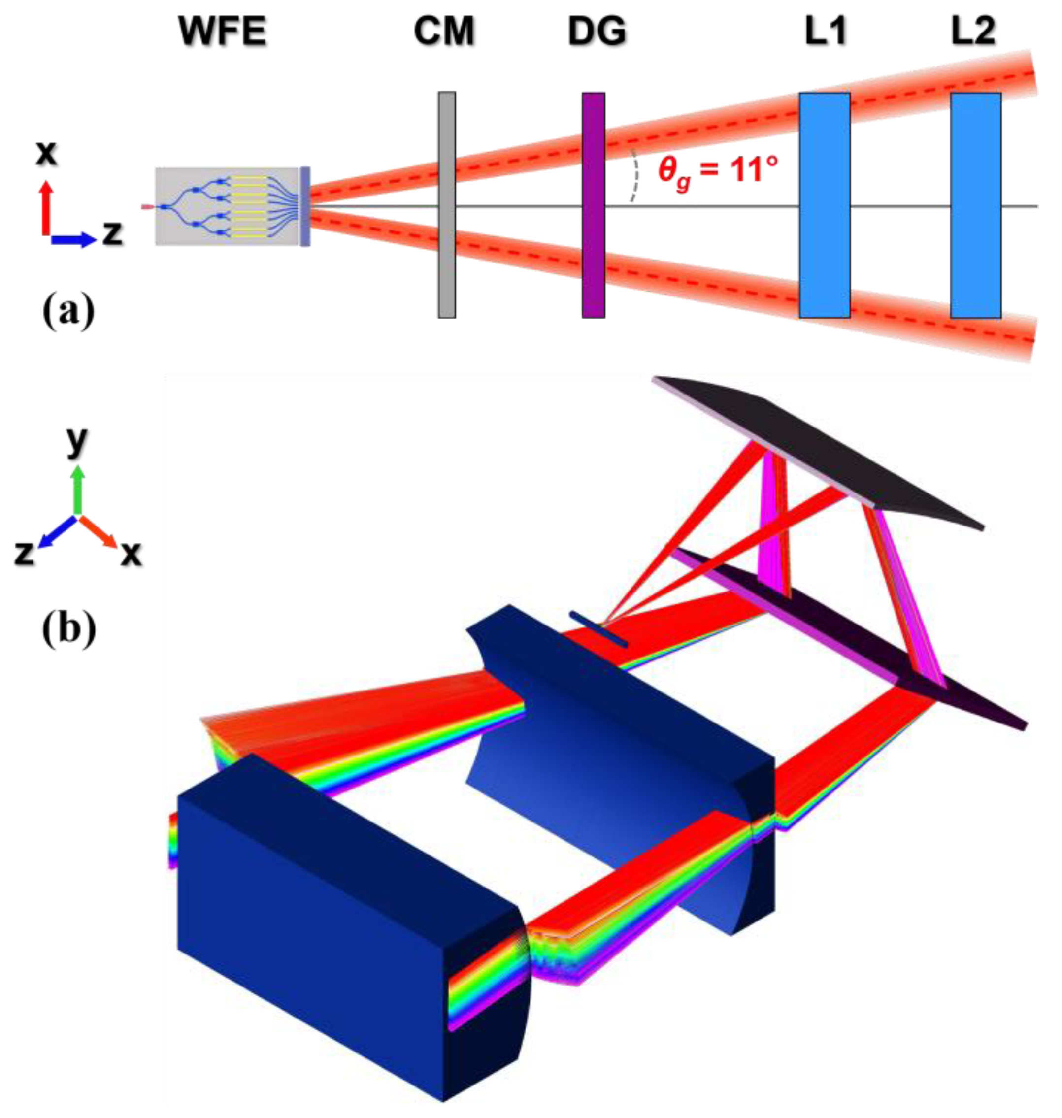
3. Optical Design of the OPA-Based WSS System with Beamsteering Capability

3.1. Beamsteering Calculations for SiN-Based OPAs

Prior to investigating the setup of the hybrid WSS that supports OPA-based beamsteering, it is essential to perform calculations regarding beamforming and steering for the SiN OPAs with varying N and d. The beam characteristics of the WFE’s input beamformers will determine the resulting channel pattern that can be imaged on the LCoS panel and thereby the operational limits that can be achieved. Figure 5 shows the FDTD calculated fields for N = 8, d = 2.5 μm, (a) φ = 0 and (b) φ = π/2, and for N = 32, d = 4 μm, (c) φ = 0 and (d) φ = π/2. As N increases, higher d values are also worth investigating for the uniform OPA. This investigation is motivated by the observation that closely packed end-fire arrays with more elements exhibit larger crosstalk due to undesired evanescent coupling of adjacent waveguides close to the facet, particularly at the fan-in section after the phase tuning stage. The value π/2 is chosen for φ in these calculations because it maintains a high peak power ratio of the main lobe compared to the grating-lobes for lower φ values. It is also essential to ensure that all θ angles of operation can be achieved for φ < π/2. When φ = π/2, the steering angle θ for N = 8 is calculated to be 9.32°, while for N = 32 it is 5.87° due to the higher d value. In addition, one of the two grating-lobes is also formed at a lower angle with increasing d. For φ = π/2, the grating-lobe with the lowest angle is formed at 26.88° for N = 8 and at 17.57° for N = 32.
Table 1 presents the calculations carried out for various combinations of N and d values, recording changes in the beam angular FWHM, steering angle, and lowest grating-lobe angle. Subsequent ray tracing simulations will be conducted using the characteristics of these input beams generated from arrays with varying N and d. All the values of Table 1 have been estimated for 1550 nm wavelength. It is worth noting that the beamwidth of each array, as well as the steering angles, are considered invariable across the wavelength range of the ITU C-band because they showed infinitesimal change in the simulations. The side-lobe level remains below 13 dB in all cases. The calculations reveal that, with φ = π/2, θ exceeds 5.8° for all N and d combinations under study. This observation indicates that any operational steering angle below this value ensures a high main lobe intensity. Additionally, the grating-lobes are formed at angles beyond 17.5°.

3.2. Hybrid WSS Enabling Beamsteering Functionality of the Frontend

To enable OPA beamsteering in the hybrid WSS, the optical system needs to be modified in such way that the variation of the angle of the input beams alters the position of the channels projected on the LCoS. In other words, the desired input angle regulates the subsequent channel routing. In the setup of Figure 2, any change of the angle of the input beam does not affect the position of the four channels and that is due to the use of the lens which guides the beam rays to the DG. Consequently, the facilitation of beamsteering can only be granted by using an optical element that does not impede this function, while also slightly focusing the rays to the DG. Figure 6a,b illustrate the schematic of the hybrid WSS on xz and yz planes, respectively, where the first cylindrical lens is substituted by a concave mirror (CM), and three lenses that are now arranged after the DG to ensure proper imaging of the channels at the LCoS. The DG is rotated by 90° compared to the previous scheme of Figure 2, with its lines now being parallel to the WFE plane. The arrangement of the DG now changes the direction of dispersion, leading to the spectral separation of the wavelengths along the y axis [27]. This also allows to steer the input beam at the xz plane without affecting the operational incident angle of the DG on the yz plane.
Figure 6c presents a perspective view of the WSS with WFE beamsteering functionality through the ray tracing simulation environment. The variation of the input angle of the source on the xz plane with respect to the optical z axis leads to a change in the position of the channel along the x axis on the LCoS panel due to the new orientation of the DG. The input beam is reflected by the CM and enters the DG with an angle equal to the input angle θ on the xz plane. The DG in this scheme has 1000 lines/mm and the angle of incidence is now 49.9° on the yz plane. The reason for choosing a DG with more lines/mm lies in the fact that, since the DG is rotated by 90° in the new scheme, the former small cone-angle of the conical beam now becomes the high cone-angle and vice-versa due to the new orientation of the lines, and thus a different DG with higher resolution is needed. Figure 6d shows the positioning of a channel at the panel with the variation of θ for the values −3°, 0°, +3°. The system is studied for the ITU 200 GHz with 24 wavelengths. Each wavelength of the 200 GHz C-band is diffracted at a different angle on the yz plane and, as a result, a beam with different wavelength illuminates a different pixelated region across the y axis. The steering with θ angle on the xz plane, in synergy with the diffraction on the yz plane, facilitates for the 2D scanning of the LCoS pixelation. It can be noticed that, as the channel moves away from the center of the panel, the holograms tend to bend upwards along the y axis, which is due to the input beam arriving with an angle θ at the DG. The CM has a radius of 70 mm, while the radii of curvature of the cylindrical lenses L1 (concave), L2 and L3 are 10 mm, 15 mm and 20 mm, and their thicknesses 4 mm, 7.8 mm and 8 mm, respectively. The distances between the components are (WFE − CM) = 20 mm, (CM − DG) = 10 mm, (DG − L1) = 20 mm, (L1 − L2) = 20 mm, (L2 − L3) = 10 mm and (L3 − LCoS) = 17 mm, and the total size of the system is 92 × 65 mm2.

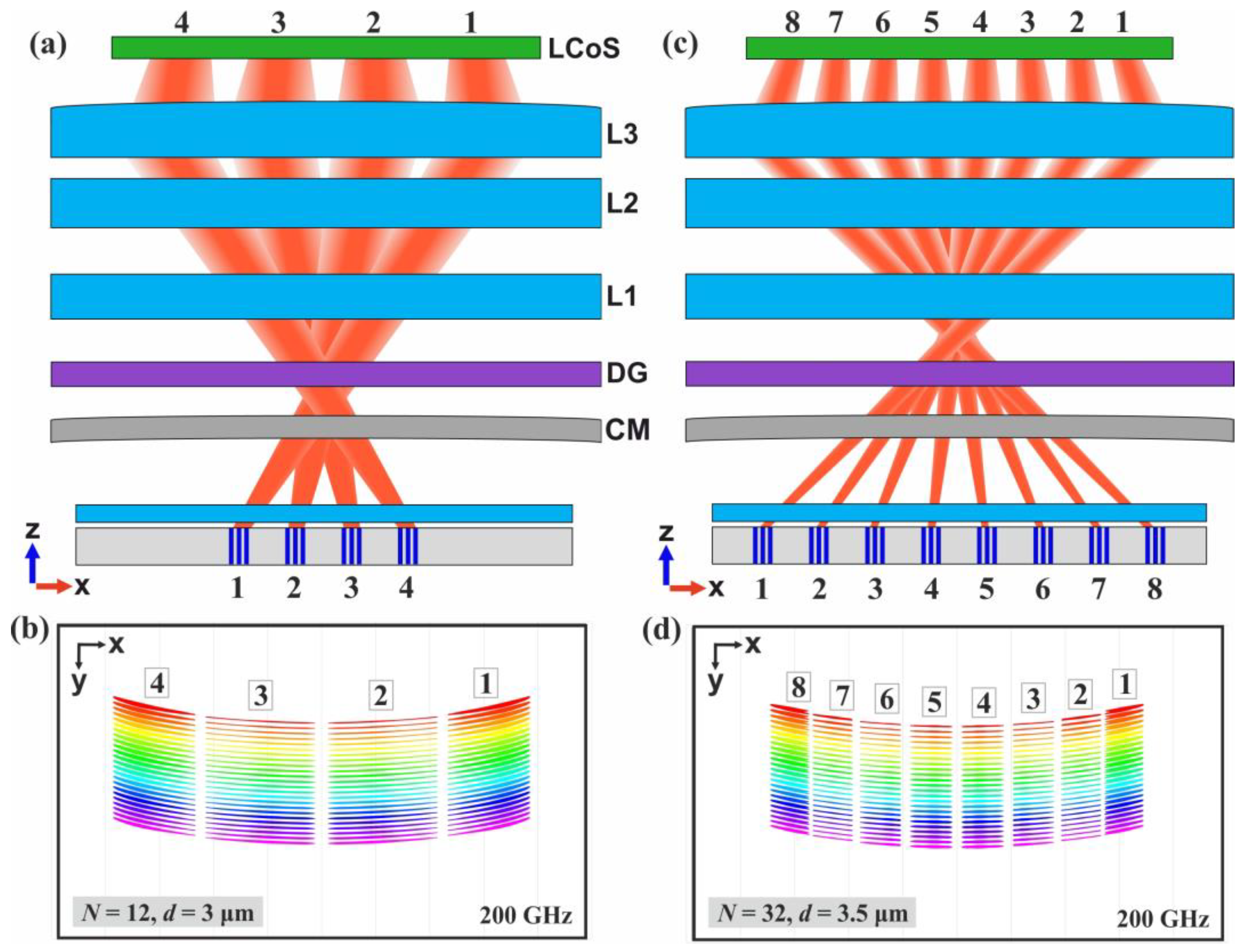
3.3. OPA Beamwidth and WSS Channels

The new arrangement of the DG does not only alter the orientation of the projected spectral channels, but also swaps the attribute that will be affected by the change in the directivity of the input beam. The beam directivity will now affect the width of each channel on the x axis, instead of the sub-hologram width on the x axis. In this under investigation WSS setup for ITU 200 GHz operation, the increase of the directivity of the input main beams will result in narrower channel width. As a consequence, the number of channels that can be displayed on the LCoS can be increased, given that the WSS will operate with an extended number of OPAs. As such, the use of waveguide arrays with greater D permits a higher number of channels to be displayed at the LCoS. This ultimately means that, by deploying OPA emitters with a specified beamwidth the hybrid WSS can be designed to support a desired number of input channels.
Ray tracing simulations explored various combinations of N and d, and Figure 7 displays the results, showcasing a distinct channel number achieved in each scenario. Employing two OPAs with N = 8 and d = 2.5 μm, Figure 7a illustrates the ray-traced model of the hybrid WSS, while Figure 7b presents the footprint diagram of the rays, revealing two channels covering a significant area of the LCoS panel. Accordingly, Figure 7c,d show four channels for N = 12 and d = 3 μm, Figure 7e,f show six channels for N = 24 and d = 3 μm, and Figure 7g,h show eight channels for N = 32 and d = 3.5 μm. Insets in each case provide close-ups of the acylindrical lens with the respective number of input beams, while the PIC of the WFEs is not depicted here. The simulations presented in Figure 7 offer a more detailed description of the proposed WSS compared to those in Figure 6, enabling an exploration of the maximum operational limit concerning N. Among the four presented scenarios, the highest value that θ needs to reach to satisfy the eight-channel condition is ±4.9°, as will be further discussed in Section 3.5 for the mixed steering scenarios.
To that end, the proper end-fire OPA geometry and choice of source dimensions determines the number of input port counts in the hybrid Mo × No WSS. In this manner, hybrid 2 × No, 4 × No, 6 × No and 8 × No WSS systems are presented through the ray tracing simulations of Figure 7. The horizontal size of the wavelength holograms ranges between 220 pixels for Mo = 2 and 1190 pixels for Mo = 8, while the vertical one ranges between 13 pixels at 1565.5 nm and 24 pixels at 1528.77 nm wavelength. The vertical distance between the sub-holograms is between 20 and 26 pixels while the horizontal distance between the channels is at least 55 pixels for all Mo cases. Based on the measurements from the footprint diagrams, the spectral separation in terms of pixel isolation is considered acceptable [22], preventing the increase of crosstalk at the LCoS panel for 200 GHz operation.

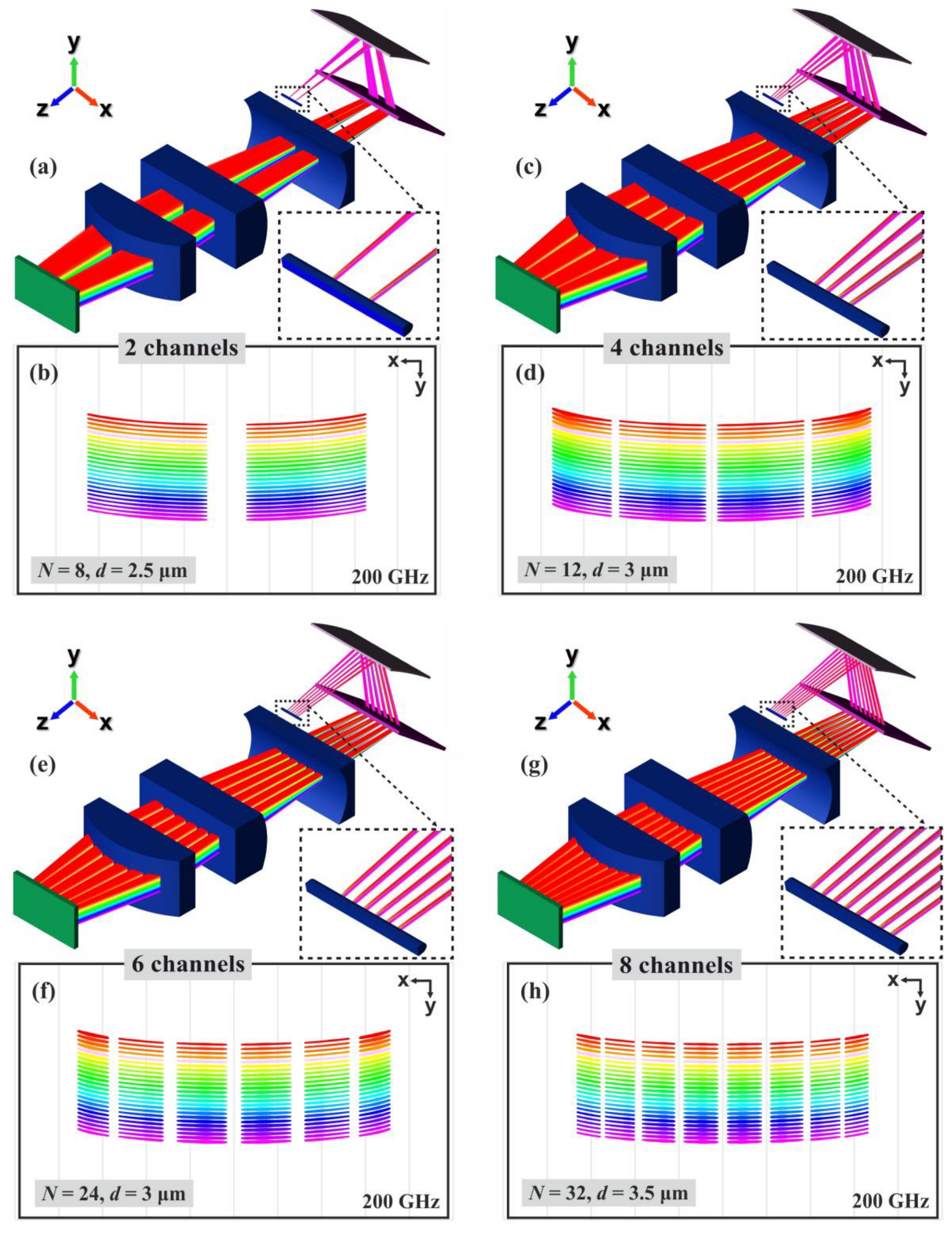
3.4. Simulation of Undesired Grating-Lobes in the Hybrid WSS

As mentioned earlier, the presence of side-lobes besides the main lobe can induce crosstalk across the LCoS below a 13 dB level from the peak power when coinciding with the channels. Another contributing factor to crosstalk would be the existence of grating-lobes appearing at 8 dB from the peak power of the main lobe according to the FDTD simulations of Section 2.1. For this reason, it is important to simulate the behavior of the grating-lobes, as well as to examine whether they would interact with the main lobes at the LCoS. In this study, two grating-lobes at angles θg are ray-traced throughout the hybrid WSS optics. In the schematic of Figure 8a, the grating-lobes are illustrated emanating from an OPA at θg = ±11°, travelling until L2, where it is clear that, beyond this point, all rays exit completely from the optical setup and do not reach L3. Figure 8b shows the simulated rays of the grating-lobes in the respective ray tracing environment for the same θg value, which is well beyond the angle calculated for all the different OPAs in Table 1. Taking into account Table 1, the simulations verify that the hybrid WSS is free from undesired grating-lobes since all OPAs feature θg ≥ 11°. The rays escape and will not interact with the remaining optical elements after L2. The PIC of the WFE is again not depicted in the latter figure for reasons of simplicity.

3.5. Channel Routing by Varying Input Beam Angles

The proposed WSS architecture is further examined by introducing input beams to the system with various input angles in such a way that the LCoS panel is illuminated by every input channel. An extreme case study is considered for both four and eight-channel counts, where the maximum angle of operation is utilized twice, illuminating the LCoS symmetrically. The ray tracing simulations of the hybrid WSS are performed with source beams of multiple OPA emitters, uniformly spaced on the WFE PIC. The optical paths of four input beams with different steering angles have been raytraced until the LCoS panel and are illustrated in Figure 9a. These beams, formed by OPAs with N = 12 and d = 3 μm, are positioned and numbered accordingly on the WFE facet, with a 0.5 mm spacing between them. The footprint diagram in Figure 9b illustrates the positions of the four channels, each labeled with the respective OPA emitter-related origin. The investigation with various input θ angles is also performed for eight OPA emitters with N = 32 and d = 3.5 μm and the illustration and results are shown in Figure 9c,d, respectively. The illumination pattern on the panel is symmetrical along the X axis, with the point of symmetry being the mid-point of the LCoS.
Table 2 provides details about the position of each OPA at the WFE, the emission angle θ for each channel, and the corresponding pixel dimensions and hologram spacing. The midpoint of each waveguide array aligns with the specified OPA position in the table, relative to the center of the WFE PIC. The steering angle θ required for the first OPA to display its input channel to the far opposite side of the LCoS represents the maximum angle of operation in each setup. In the configuration of Figure 9a, the highest θ can reach up to ±4.6°, while in the configuration of Figure 9c, it can go up to ±4.9°. All beams incident on the LCoS panel arrive at its active surface with an angle below 10°, preventing unnecessary reflections. Moreover, considering the outcomes of Table 1, a φ value less than π/2 is necessary to achieve the maximum θ in both displayed scenarios. This arguably means that the hybrid WSS is designed to operate at small OPA steering angles in order to achieve the flexible spectral illumination profile at the LCoS panel, contrary to LiDAR systems with a very high number of elements [28,29] that target a large field of view and a very narrow main beam. The previous analysis explains why OPAs with small N are suitable for WSSs with beamsteering capabilities.
The hologram size of each channel is measured along both the X and Y axes at the LCoS plane. On the X axis, the size decreases with N, remains independent of the wavelength, and exhibits larger dimensions for outer holograms compared to inner ones due to the upward bending induced by the incidence of the rays with angle θ on the DG. For the 4 channels scenario, the X size is either 634 or 845 pixels, while for the 8-channel one, it ranges between 296 and 320 pixels. For the Y axis, the hologram size varies based on wavelength, X position, and θ, ranging between 9 ± 4 and 28 ± 3 pixels for the 4 channels and between 9 ± 4 and 25 ± 4 pixels for the 8 channels. These Y size values account for the thickest region of the holograms. Similarly, the spacing between holograms on the Y axis varies, considering the distance between the thickest hologram regions, ranging between 12 ± 2 and 29 ± 6 pixels for the 4 channels and between 14 ± 3 and 33 ± 5 pixels for the 8 channels. Image measurements on the panel confirm that, for any supported channel emerging from an input beam at a θ angle, all wavelength sub-hologram pixelations are clearly distinct and do not overlap on any area of the panel. In other schemes with diverse steering angles, different from the presented extreme case study, hologram sizes and spacings do not fall below the minimum values recorded in Table 2, and their pixelations also remain clearly distinguished.
To sum up, the study of the hybrid WSS based on SiN OPA emitters reveals that more directive input source beams bring benefits to both straight and steering enabled layouts. For the null-steering layout, a higher-N SiN OPA structure results in better spectrally resolved wavelengths at the LCoS, allowing to project clearly even 48 channels at a 100 GHz spacing. For the steering-enabling layout, narrower input beams allow the hybrid WSS to support more input channels for 200 GHz operation, reaching an 8 × No port count while handling steering angles up to ±4.9°. The wavelength holograms are well distinguishable and isolated, and the ray tracing simulations further confirm that the hybrid WSS is free from grating-lobes, with the primary source of crosstalk being the 13 dB side-lobes. Considering all the above, the findings of this study illustrate the feasibility of designing novel hybrid WSS systems with frontends comprised of end-fire OPA-based emitters. To that end, the work highlights the prospect of exploiting OPAs in future wireless communication links and WDM systems, as well as the importance of addressing the capabilities of such systems in terms of electromagnetic and ray tracing design to unlock their full potential.

4. Misalignment Tolerance Study

The tolerance to alignment errors is evaluated by misaligning the most critical component in terms of alignment precision which is the acylindrical lens of the WFE. Sub-micrometer precision is typically required for the accurate positioning of the microlenses in hybrid optical systems, where alignment steps of 0.1 μm are achievable [30]. In this study, the acylindrical lens will be angularly misaligned on the xz plane with respect to the WFE PIC with 8 OPAs by a step of 0.5 μm, a value that can also be detected by a camera during the alignment procedure [31]. Figure 10a illustrates the misaligned acylindrical lens in front of the WFE PIC, where the ±Δxm misplacement at the lens’ sides corresponds to an angle of ±θm. Both PIC and lens are considered to be 5 mm wide. As the angular misalignment θm increases, the wavelength holograms become distorted. This distortion is more intense for the beams coming from OPAs that are closer to the sides of the lens, where Δxm is larger. Figure 10b–e show the footprint diagrams for θm = 0°, θm = 0.0115°, θm = 0.0229° and θm = 0.0343°, respectively, as Δx increases from 0 to 1.5 μm with the 0.5 μm step. The results reveal that the holograms are well distinguished until Δxm reaches 1 μm, where a minor overlap of 1 to 2 pixels appears at the wavelengths at the first and last channels. For a Δx of 1.5 μm the number of overlapping pixels between neighboring wavelengths is extended to 15 for the first and last channels, and to 14 and 4 for the two adjacent left channels. The pixelated area illuminated by overlapping wavelengths can potentially increase the crosstalk level of output ports should it be left unhandled. The unwanted light can be attenuated by tuning the phase shift of the LCoS pixels so that the light is directed to a region that is free from output ports. As a consequence, apart from the possibly increased crosstalk level, the misalignment can also increase the total optical losses of the system, since a fraction of the holograms’ area will need to be disregarded.
In addition, the study showed that the WFE PIC is more tolerant to mispositioning at the y axis in respect to the microlens, as well as to a lens tilt along the x axis. A misplacement of up to 3 μm or a tilt of up to 3.5° of the acylindrical lens, as illustrated in Figure 10f, can be tolerated, without causing any spectral overlap of adjacent holograms. The misfabrication of the acylindrical lens is not taken into account. Moreover, a misposition of up to 2.5 mm in the z axis can be tolerated for one of the lenses of the setup, while the angular misalignment of the CM or the DG at any axis needs to be below 1.5°, as shown in Figure 10g. Overall, the study points out that the misalignment of the acylindrical lens ought to be kept at a minimum, but a range of ±0.5 μm is acceptable. The precise alignment of the rest of the optical components can be safely considered feasible during the assembly process.

5. Discussion

The motivation for investigating multiple OPAs on a single SiN chip lies on the exciting prospect of realizing effective simultaneous transmission of numerous optical signals through the control of diverse-beam emitters in a centimeter-scale network device. It is worth pointing out that the proposed novel hybrid WSS displays both some common features and some differences to the work of Kim et al. [10], where a polymer-based OPA with 32 waveguide elements was demonstrated. In terms of architecture, both OPAs emit the main beam in an end-fire scheme with a cylindrical lens placed directly in front of the PICs’ facets, and both scan in a 2D way employing a diffraction grating. However, in the present work, beamforming is investigated for various cases with up to 32 elements, and the imaging optics setup is designed in a such way that the beams adapt and illuminate a pixelated LCoS panel across their steering range. In terms of performance, the calculated 13 dB side-lobe level in the present work is lower compared to the polymer counterpart, signifying less optical crosstalk. In addition, the maximum steering angles of 4.9° provided by the SiN OPA PIC, even though restricted for the operational purposes of the hybrid WSS, are higher compared to the polymer counterpart with 3.9° prior to the diffraction grating. These differences in the maximum steering angle and the side-lobe level are associated with the higher index contrast that SiN waveguides typically have compared to polymer waveguides. This offers them higher confinement, allowing them to be arranged more compactly, with lower cross-coupling, at the edge of the OPA PIC, and to enhance beamforming.
A common method to generate end-fire arrays of waveguides is by utilizing splitter trees [32]. The array with N = 32 can be realized with five stages of 1 × 2 splitters, while the N = 12 array with two stages of 1 × 2 and a third stage of 1 × 3 splitters. The phase shifters are placed along the waveguide array prior to the emission. After the phase tuning stage, the array of waveguides typically fans-in in order to achieve the desired emitter’s pitch (D). It is important to note that the spacing between the phase shifters at the phase tuning stage plays a significant role to the total size of the OPA PIC. In TO phase shifters, the heating wires must be placed apart with a sufficient distance between them to avoid any thermal crosstalk [33], while in EO modulators the high integration density can induce electrical crosstalk [34]. Chip size dimensions of 5 × 5 mm2, or 10 × 5 mm2 in the worst case of eight OPAs with N = 32, suffice in order to generate the splitter trees and arrays, and place the phase shifters and metal routing. The insertion of light to the input SiN waveguide of each OPA structure can be realized in a butt-coupling scheme by deploying an inverse taper-based spot size converter aligned with a polarization maintaining single mode fiber [35].
As for the vertical divergence of the input beams, it is a key factor to consider when selecting a design for the lens positioned in front of the PIC. It is possible to reduce the vertical divergence of the input beams by applying a tapered waveguide geometry with a taper tip width smaller than 1 μm at the facet of the end-fire OPA [36]. In this way, a lens with a lower acceptance angles could be used in front of the WFE SiN PIC, potentially reducing the need for a sophisticated lens design without sacrificing the total number of supported wavelengths of each input channel.
The phase modulation technology plays a significant role in the overall performance and scale of the OPA PIC. OPAs in general exhibit a linear increase in power drain as the number of waveguide elements increases. Therefore, apart from a larger required PIC area, a SiN array with 32 elements would have a four times higher electrical power consumption than one with 8 elements. Eventually, a hybrid Mo × No WSS would consume more power as Mo increases. At this stage, it is worth noting various phase tuning technologies on the SiN material platform. Thermo-optic (TO) phase shifting with metal heaters can exhibit power consumption for π phase shift (Pπ) close to a few mW [37,38,39,40], with very low optical losses and a typical length of ~1 mm. Hybrid PICs with Barium Titanate (BatTiO3 or BTO)SiN–based electro-optic (EO) phase modulators, utilizing the Pockels effect, can drastically reduce Pπ to a μW or nW scale and achieve high modulation speed at the cost of high propagation losses at a similar length scale [41,42]. Thin film Lithium Niobate (LiNbO3 or LNO)Si–N hybrid PICs similarly display very low switching energy with nJ values and high speed at the expense of high optical losses for ~mm long structures [43,44,45]. Graphene based heaters have recently demonstrated TO phase shifting with nJ scale consumption and sub-μs switching time for μm long modulators, albeit compromised by very high propagation and insertion losses [46,47,48,49]. Moreover, the SiN-Si transition in a monolithically integrated multilayer hybrid platform allows for the efficient TO and EO phase tuning at Si level while taking advantage of the low propagation losses of SiN [50].
Throughout the work, it is recognized that the major source of optical crosstalk in the setup is the side-lobes, which may illuminate any area across the LCoS depending on the input angle of the emitter. However, as mentioned, the 13 dB level of the side lobes is not expected to induce significant crosstalk to the other channels. Nonetheless, there are certain techniques reported in the literature that can be used to suppress them, such as deploying a non-uniform waveguide array [51] or tuning the phases of the waveguides [52]. In addition, phase mismatching of adjacent non-uniform waveguide emitters can be applied to keep the evanescent coupling between them to a minimum prior to the emission [53]. All the waveguide structure modifications mentioned above could undeniably enhance the system performance overall, but they fall beyond the scope of this work, since they would require additional dedicated and extensive simulations. The operation of the proposed novel hybrid switch was comprehensively studied with the use of ray tracing simulations, handling beams emanating from uniform SiN optical phased arrays with properties evaluated by FDTD simulations.

6. Conclusions

In this work, we demonstrated the design of a new hybrid WSS system that exploits end-fire SiN OPAs in its frontend for adding a new dimension to its routing capabilities. The study of the OPA-based WFE with null-steering into a conventional WSS optical setup showed that the decrease in the input beams’ dimensions results in better spectrally resolved channels on the LCoS panel and can shift the operation from 200 GHz with 24 wavelengths to 100 GHz with 48 wavelengths in the ITU C-band. The layout is then modified in such way that, with the use of a concave mirror, it enables the OPA beamsteering functionality, allowing each of the input channels to illuminate various pixelated areas of the LCoS panel. As the input beams become narrower, the number of available input channels increases, and the WSS achieves up to an 8 × No routing port count. The proposed WSS can effectively operate using OPA steering angles up to ±4.9° and it is unaffected by undesired grating-lobes. The optical crosstalk at the LCoS panel due to the side-lobe level is 13 dB, while the crosstalk due to channel overlapping is minimized by ensuring that the wavelength sub-holograms are well-isolated at the panel’s pixelation. The tolerance to misalignment study indicated that the most critical component is the acylindrical lens in front of the WFE PIC and that a misposition range of ±0.5 μm is tolerable. Such advancements demonstrate the promising potential of integrating OPAs into hybrid WSS systems, as well as to future wireless communication and centimeter-scale WDM network links.

Author Contributions

G.P. conducted the research and analysis and wrote the paper, D.K. and D.C. aided in simulations and proofreading, and K.V. supervised. All authors have read and agreed to the published version of the manuscript.

Funding

This research received no external funding.

Institutional Review Board Statement

Not applicable.

Informed Consent Statement

Not applicable.

Data Availability Statement

All data generated during this work can be obtained from the corresponding author upon reasonable request.

Conflicts of Interest

The authors declare no conflicts of interest.

References

  1. Kozdrowski, S.; Żotkiewicz, M.; Sujecki, S. Optimization of Optical Networks Based on CDC-ROADM Technology. Appl. Sci. 2019, 9, 399. [Google Scholar] [CrossRef]
  2. Li, Y.; Gao, L.; Shen, G.; Peng, L. Impact of ROADM colorless, directionless, and contentionless (CDC) features on optical network performance [Invited]. J. Opt. Commun. Netw. 2012, 4, B58–B67. [Google Scholar] [CrossRef]
  3. Yamamoto, S.; Taniguchi, H.; Kisaka, Y.; Camatel, S.; Ma, Y.; Ogawa, D.; Hadama, K.; Fukutoku, M.; Goh, T.; Suzuki, K. First demonstration of a C  +  L band CDC-ROADM with a simple node configuration using multiband switching devices. Opt. Express 2021, 29, 36353–36365. [Google Scholar] [CrossRef] [PubMed]
  4. Xie, D.; Wang, D.; Zhang, M.; Liu, Z.; You, Q.; Yang, Q.; Yu, S. LCoS-Based Wavelength-Selective Switch for Future Finer-Grid Elastic Optical Networks Capable of All-Optical Wavelength Conversion. IEEE Photonics J. 2017, 9, 7101212. [Google Scholar] [CrossRef]
  5. Robertson, B.; Yang, H.; Redmond, M.M.; Collings, N.; Moore, J.R.; Liu, J.; Jeziorska Chapman, A.M.; Pivnenko, M.; Lee, S.; Wonfor, A.; et al. Demonstration of Multi-Casting in a 1 × 9 LCOS Wavelength Selective Switch. J. Light. Technol. 2014, 32, 402–410. [Google Scholar] [CrossRef]
  6. Huang, Z.; Yang, S.; Zheng, Z.; Pan, X.; Li, H.; Yang, H. Highly Compact Twin 1 × 35 Wavelength Selective Switch. J. Light. Technol. 2023, 41, 233–239. [Google Scholar] [CrossRef]
  7. Yang, H.; Wilkinson, P.; Robertson, B.; Giltrap, S.; Snowdon, O.; Prudden, H.; Chu, D. 24 [1 × 12] Wavelength Selective Switches Integrated on a Single 4k LCoS Device. J. Light. Technol. 2021, 39, 1033–1039. [Google Scholar] [CrossRef]
  8. Suzuki, K.; Seno, K.; Ikuma, Y. Application of Waveguide/Free-Space Optics Hybrid to ROADM Device. J. Light. Technol. 2017, 35, 596–606. [Google Scholar] [CrossRef]
  9. Sakamaki, Y.; Shikama, K.; Ikuma, Y.; Suzuki, K. Wavelength selective switch array employing silica-based waveguide frontend with integrated polarization diversity optics. Opt. Express 2017, 25, 19946–19954. [Google Scholar] [CrossRef]
  10. Kim, S.M.; Lee, E.S.; Chun, K.W.; Jin, J.; Oh, M.C. Compact solid-state optical phased array beam scanners based on polymeric photonic integrated circuits. Sci. Rep. 2021, 11, 10576. [Google Scholar] [CrossRef]
  11. Li, Y.; Chen, B.; Na, Q.; Tao, M.; Liu, X.; Zhi, Z.; Peng, T.; Li, X.; Luo, X.; Lo, G.; et al. High-Data-Rate and Wide-Steering-Range Optical Wireless Communication Via Nonuniform-Space Optical Phased Array. J. Light. Technol. 2023, 41, 4933–4940. [Google Scholar] [CrossRef]
  12. Di, Y.; Sun, C.; Chen, S.; Liu, W.; Dai, Y.; Li, B.; Shi, W.; Lin, J.; Shao, Y.; Xu, J.; et al. Capacity Enhancement of VLC by Blue-green Wavelength Division Multiplexing Using Optical Phased Array. In Proceedings of the 2023 Optical Fiber Communications Conference and Exhibition (OFC), San Diego, CA, USA, 5–9 March 2023; p. M4F.2. [Google Scholar]
  13. Bauters, J.F.; Heck MJ, R.; John, D.; Dai, D.; Tien, M.-C.; Barton, J.S.; Leinse, A.; Heideman, R.G.; Blumenthal, D.J.; Bowers, J.E. Ultra-low-loss high-aspect-ratio Si3N4 waveguides. Opt. Express 2011, 19, 3163–3174. [Google Scholar] [CrossRef] [PubMed]
  14. Li, Z.; Fan, Z.; Zhou, J.; Cong, Q.; Zeng, X.; Zhang, Y.; Jia, L. Process Development of Low-Loss LPCVD Silicon Nitride Waveguides on 8-Inch Wafer. Appl. Sci. 2023, 13, 3660. [Google Scholar] [CrossRef]
  15. Liu, J.; Huang, G.; Wang, R.N.; He, J.; Raja, A.S.; Liu, T.; Engelsen, N.J.; Kippenberg, T.J. High-yield, wafer-scale fabrication of ultralow-loss, dispersion-engineered silicon nitride photonic circuits. Nat. Commun. 2021, 12, 2236. [Google Scholar] [CrossRef]
  16. Tien, M.-C.; Bauters, J.F.; Heck MJ, R.; Blumenthal, D.J.; Bowers, J.E. Ultra-low loss Si3N4 waveguides with low nonlinearity and high power handling capability. Opt. Express 2010, 18, 23562–23568. [Google Scholar] [CrossRef]
  17. Volakis, J.L. Antenna Engineering Handbook, 4th ed.; McGraw-Hill Education: New York, NY, USA, 2007; Chapter One; p. 21. [Google Scholar]
  18. Balanis, C.A. Antenna Theory: Analysis and Design, 4th ed.; Wiley: Hoboken, NJ, USA, 2016; pp. 293–297. [Google Scholar]
  19. Ji, H.; Shan, Y.; Mo, Y.; Chen, Z.; Ma, D. Optical Design of an LCoS-Based 1 × 10 WSS with High Coupling Efficiency and Compact Light Paths. Photonics 2023, 10, 1107. [Google Scholar] [CrossRef]
  20. Schifano, L.; Berghmans, F.; Dewitte, S.; Smeesters, L. Optical Design of a Novel Wide-Field-of-View Space-Based Spectrometer for Climate Monitoring. Sensors 2022, 22, 5841. [Google Scholar] [CrossRef]
  21. Zeng, C.; Han, Y.; Liu, B.; Sun, P.; Li, X.; Chen, P. Optical design of a high-resolution spectrometer with a wide field of view. Opt. Lasers Eng. 2021, 140, 106547. [Google Scholar] [CrossRef]
  22. Hu, Y.; Chang, J.; Ji, Z.; Chen, W.; Li, Y.; Li, D. Construction method for designing a spectrometer with variable spectral resolution and wide bandwidth using multiple off-axis convex gratings. Opt. Express 2022, 30, 2472–2486. [Google Scholar] [CrossRef]
  23. Peatross, J.; Ware, M. Physics of Light and Optics; Brigham Young University: Provo, UT, USA, 2015; pp. 236–247. [Google Scholar]
  24. Website of the Commercial LCoS SLM. Available online: https://holoeye.com/products/spatial-light-modulators/gaea-2-phase-only/ (accessed on 1 June 2023).
  25. Website of the Commercial Diffraction Grating. Available online: https://ibsen.com/products/transmission-gratings/ping-telecom-gratings/ (accessed on 1 June 2023).
  26. Yunshu, G.; Xiao, C.; Genxiang, C.; Ying, C.; Qiao, C.; Feng, X.; Yiquan, W. 1 × 25 LCOS-based wavelength selective switch with flexible passbands and channel selection. Opt. Fiber Technol. 2018, 45, 29–34. [Google Scholar]
  27. Muttikulangara, S.S.; Baranski, M.; Rehman, S.; Hu, L.; Miao, J. Diffraction grating integrated on micromachined stepper motor for diversity implementation in imaging spectroscopy. In Proceedings of the 2018 IEEE Micro Electro Mechanical Systems (MEMS), Belfast, UK, 21–25 January 2018; pp. 696–699. [Google Scholar]
  28. Poulton, C.V.; Byrd, M.J.; Russo, P.; Moss, B.; Shatrovoy, O.; Khandaker, M.; Watts, M.R. Coherent LiDAR With an 8192-Element Optical Phased Array and Driving Laser. IEEE J. Sel. Top. Quantum Electron. 2022, 28, 6100508. [Google Scholar] [CrossRef]
  29. Zhang, X.; Kwon, K.; Henriksson, J.; Luo, J.; Wu, M.C. A large-scale microelectromechanical-systems-based silicon photonics LiDAR. Nature 2022, 603, 253–258. [Google Scholar] [CrossRef] [PubMed]
  30. Das, A.N.; Sin, J.; Popa, D.O.; Stephanou, H.E. On the precision alignment and hybrid assembly aspects in manufacturing of a microspectrometer. In Proceedings of the 2008 IEEE International Conference on Automation Science and Engineering, Arlington, VA, USA, 23–26 August 2008; Institute of Electrical and Electronics Engineers (IEEE): Piscataway, NJ, USA; pp. 959–966. [Google Scholar]
  31. Mohaupt, M.; Beckert, E.; Eberhardt, R.; Tünnermann, A. Alignment Procedures for Micro-optics. In IFIP Advances in Information and Communication Technology; Springer: Berlin/Heidelberg, Germany, 2010; Volume 315, pp. 143–150. [Google Scholar]
  32. Poulton, C.V.; Byrd, M.J.; Raval, M.; Su, Z.; Li, N.; Timurdogan, E.; Coolbaugh, D.; Vermeulen, D.; Watts, M.R. Large-scale silicon nitride nanophotonic phased arrays at infrared and visible wavelength. Opt. Lett. 2017, 42, 21–24. [Google Scholar] [CrossRef] [PubMed]
  33. Yao, W.; Gilardi, G.; Calabretta, N.; Smit, M.K.; Wale, M.J. Experimental and Numerical Study of Electrical Crosstalk in Photonic-Integrated Circuits. J. Light. Technol. 2015, 33, 934–9425. [Google Scholar] [CrossRef]
  34. Jacques, M.; Samani, A.; El-Fiky, E.; Patel, D.; Xing, Z.; Plant, D.V. Optimization of thermo-optic phase-shifter design and mitigation of thermal crosstalk on the SOI platform. Opt. Express 2019, 27, 10456–10471. [Google Scholar] [CrossRef] [PubMed]
  35. Brunetti, G.; Heuvink, R.; Schreuder, E.; Armenise, M.N.; Ciminelli, C. Silicon Nitride Spot Size Converter With Very Low-Loss Over the C-Band. IEEE Photonics Technol. Lett. 2023, 22, 1215–1218. [Google Scholar] [CrossRef]
  36. Bhandari, B.; Wang, C.; Gwon, J.Y.; Heo, J.M.; Ko, S.Y.; Oj, M.C.; Lee, S.S. Dispersive silicon–nitride optical phased array incorporating arrayed waveguide delay lines for passive line beam scanning. Sci. Rep. 2022, 12, 18759. [Google Scholar] [CrossRef] [PubMed]
  37. Idres, S.; Hashemi, H. Low-Power SiN Thermo-Optic Phase Modulator Operating in Red Visible Wavelength Range. In Proceedings of the Conference on Lasers and Electro-Optics: Applications and Technology 2020, Washington, DC, USA, 10–15 May 2020; pp. 1–2. [Google Scholar]
  38. Yong, Z.; Chen, H.; Luo, X.; Govdeli, A.; Chua, H.; Azadeh, S.S.; Stalmashonak, A.; Lo, G.Q.; Poon, J.K.S.; Sacher, W.D. Power-efficient silicon nitride thermo-optic phase shifters for visible light. Opt. Express 2022, 30, 7225. [Google Scholar] [CrossRef]
  39. Wu, Z.; Lin, S.; Yu, S.; Zhang, Y. Submilliwatt Silicon Nitride Thermo-Optic Modulator Operating at 532 nm. Photonics 2024, 11, 213. [Google Scholar] [CrossRef]
  40. Alemany, R.; Muñoz, P.; Pastor, D.; Domínguez, C. Thermo-Optic Phase Tuners Analysis and Design for Process Modules on a Silicon Nitride Platform. Photonics 2021, 8, 496. [Google Scholar] [CrossRef]
  41. Ortmann, J.E.; Eltes, F.; Caimi, D.; Meimer, N.; Demkov, A.A.; Czornomaz, L.; Fompeyrine, J.; Abel, S. Ultra-Low-Power Tuning in Hybrid Barium Titanate–Silicon Nitride Electro-optic Devices on Silicon. ACS Photonics 2019, 6, 2677–2684. [Google Scholar] [CrossRef]
  42. Kohli, M.; Chelladurai, D.; Messner, A.; Horst, Y.; Moor, D.; Winiger, J.; Blatter, T.; Buriakova, T.; Convertino, C.; Eltes, F.; et al. Plasmonic Ferroelectric Modulator Monolithically Integrated on SiN for 216 GBd Data Transmission. J. Light. Technol. 2023, 41, 3825–3831. [Google Scholar] [CrossRef]
  43. Ahmed AN, R.; Nelan, S.; Shi, S.; Yao, P.; Mercante, A.; Prather, D.W. Subvolt electro-optical modulator on thin-film lithium niobate and silicon nitride hybrid platform. Opt. Lett. 2020, 45, 1112–1115. [Google Scholar] [CrossRef] [PubMed]
  44. Lee, W.B.; Kwon, Y.J.; Kim, D.H.; Sunwoo, Y.H.; Lee, S.S. Hybrid integrated thin-film lithium niobate–silicon nitride electro-optical phased array incorporating silicon nitride grating antenna for two-dimensional beam steering. Opt. Express 2024, 32, 9171–9183. [Google Scholar] [CrossRef] [PubMed]
  45. Wang, Z.; Li, X.; Ji, J.; Sun, Z.; Sun, J.; Fang, B.; Lu, J.; Li, S.; Ma, X.; Chen, X.; et al. Fast-speed and low-power-consumption optical phased array based on lithium niobate waveguides. Nanophotonics 2024. [Google Scholar] [CrossRef]
  46. Qiu, C.; Yang, Y.; Li, C.; Wang, Y.; Wu, K.; Chen, J. All-optical control of light on a graphene-on-silicon nitride chip using thermo-optic effect. Sci. Rep. 2017, 7, 17046. [Google Scholar] [CrossRef]
  47. Ji, L.; Chen, W.; Gao, Y.; Xu, Y.; Wu, C.; Wang, X.; Yi, Y.; Li, B.; Sun, X.; Zhang, D. Low-power electro–optic phase modulator based on multilayer graphene/silicon nitride waveguide. Chin. Phys. B 2020, 29, 084207. [Google Scholar] [CrossRef]
  48. Brunetti, G.; Conteduca, D.; Dell’Olio, F.; Ciminelli, C.; Armenise, M.N. Design of an ultra-compact graphene-based integrated microphotonic tunable delay line. Opt. Express 2018, 26, 4593–4604. [Google Scholar] [CrossRef]
  49. Capmany, J.; Domenech, D.; Muñoz, P. Silicon Graphene Reconfigurable CROWS and SCISSORS. IEEE Photonics J. 2015, 7, 2700609. [Google Scholar] [CrossRef]
  50. Sacher, W.D.; Mikkelsen, J.C.; Huang, Y.; Mak JC, C.; Yong, Z.; Luo, X.; Li, Y.; Dumais, P.; Jiang, J.; Goodwill, D.; et al. Monolithically Integrated Multilayer Silicon Nitride-on-Silicon Waveguide Platforms for 3-D Photonic Circuits and Devices. Proc. IEEE 2018, 106, 2232–2245. [Google Scholar] [CrossRef]
  51. Hulme, J.C.; Doylend, J.K.; Heck MJ, R.; Peters, J.D.; Davenport, M.L.; Bovington, J.T.; Coldren, L.A.; Bowers, J.E. Fully integrated hybrid silicon two dimensional beam scanner. Opt. Express 2015, 23, 5861–5874. [Google Scholar] [CrossRef] [PubMed]
  52. He, X.; Dong, T.; He, J.; Xu, Y. A Design Approach of Optical Phased Array with Low Side Lobe Level and Wide Angle Steering Range. Photonics 2021, 8, 63. [Google Scholar] [CrossRef]
  53. Kim, Y.; Yoon, H.; You, J.-B.; Kim, M.; Park, H.-H. Wide-Angle Beam-Steering Using an Optical Phased Array with Non-Uniform-Width Waveguide Radiators. Photonics 2020, 7, 56. [Google Scholar] [CrossRef]
Figure 1. (a) The uniformly spaced waveguides of the SiN OPA consisting of N elements. The smaller figure on the right side is a simple illustration of the beam emission. (b) Electric field profile at the OPA’s facet and (c) the beam intensity at 100 μm distance from the edge of the PIC for N = 4. The corresponding field (d) and intensity (e) for N = 8. Beam far-field propagation across the xz plane at 100 μm distance from the edge of the PIC for (f) N = 4 and (g) N = 8.
Photonics 11 00381 g001
Figure 2. Schematic diagram of the hybrid WSS with an OPA-based frontend: (a) xz plane and (b) yz plane. The wavelengths are separated on the xz plane. (c) Simulated ray tracing model of the WSS where four input source beams are spectrally separated at the LCoS panel.
Photonics 11 00381 g002
Figure 3. Rays’ footprint diagram at the LCoS of 24 wavelengths of the 200 GHz ITU C-Band with varying number of waveguide elements of the WFE’s emitters: (a) N = 4, (b) N = 8, (c) N = 12 and (d) N = 16. The increase of N leads to a better spectral separation and the insets with dashed lines at each channel indicate the close-up inspection presented below each diagram.
Photonics 11 00381 g003
Figure 4. Rays’ footprint diagram at the LCoS of 48 wavelengths of the 100 GHz ITU C-Band for (a) N = 12 and (b) N = 16 waveguide elements of the WFE’s emitters. The spacing between the holograms is higher for N = 16, resulting in better resolved channels.
Photonics 11 00381 g004
Figure 5. FDTD calculated far-field beam patterns of the uniform SiN OPA for φ = 0 and φ = π/2, respectively, for (a,b) N = 8, d = 2.5 μm and (c,d) N = 32, d = 4 μm. The increase of d results in lower steering angles.
Photonics 11 00381 g005
Figure 6. Schematic diagram of the hybrid WSS utilizing OPA beamsteering within its frontend: (a) xz plane and (b) yz plane. The steering is realized on the xz plane, and the wavelengths are separated on the yz plane. (c) Simulated ray tracing model of the OPA-beamsteering based WSS with an input source beam steered at an angle θ. (d) The pattern of the channel for θ = −3°, 0°, 3°.
Photonics 11 00381 g006
Figure 7. Ray tracing simulated model of the hybrid WSS and the footprint diagram at the LCoS panel, respectively, for (a,b) 2 channels, (c,d) 4 channels, (e,f) 6 channels and (g,h) 8 channels. The insets show close-up images of the corresponding number of input source-beams.
Photonics 11 00381 g007
Figure 8. (a) The schematic of the OPA-steering based hybrid WSS on the xz plane depicts two grating-lobes at angles θg = 11° escaping the optical system after the lens L2. (b) The corresponding ray-traced model shows the behavior of the OPAs’ grating-lobes at θg = 11°.
Photonics 11 00381 g008
Figure 9. (a) Graphical representation of 4 input beams on the xz plane with mixed input angles, and (b) the corresponding channel pattern of each beam at the LCoS panel. In (c,d) the respective illustration and results for 8 input source beams with mixed angles are shown.
Photonics 11 00381 g009
Figure 10. (a) Schematic showing the angular misalignment θm of the acylindrical lens on the xz plane, misplaced by ±Δxm at each side. The distortion of the footprint diagram at the LCoS with increasing misalignment: (b) θm = 0°, (c) θm = 0.0115°, (d) θm = 0.0229° and (e) θm = 0.0343°. (f) Maximum allowable y axis misplacement and tilt of the acylindrical lens and (g) misalignment between the optical elements and angular misalignment of the CM and DG.
Photonics 11 00381 g010
Table 1. Calculated SiN OPA beam characteristics with varying N and d. The number of the achieved WSS channels is noted based on the ray tracing simulations.
Grating-Lobe Angle
(for φ = π/2)
Steering Angle θ (for φ = π/2)Main Beam FWHMTotal Length D (μm)Spacing d (μm)N
26.88°
23.54°
9.32°
7.82°
4.16°
3.47°
18.5
22
2.5
3
8
28.46°
23.61°
9.41°
7.82°
2.77°
2.31°
28.5
34
2.5
3
12
23.56°
20.19°
7.81°
6.82°
1.75°
1.46°
46
53.5
3
3.5
16
23.60°
20.17°
7.85
6.73°
1.22°
1.12°
70
81.5
3
3.5
24
20.23°
17.57°
6.70°
5.87°
0.84°
0.72°
109.5
125
3.5
4
32
Table 2. Position of the OPAs at the WFE and their corresponding input beam angles for each channel on the LCoS panel for the cases of N = 12 and N = 32.
4 Channels (N = 12, d = 3 μm)
Ch. number1234
OPA Position (mm)−0.75−0.250.250.75
Angle θ4.6°1.55°−1.55°−4.6°
Hologram X size (px)634845845634
Hologram Y size (px)28 ± 39 ± 428 ± 39 ± 4
Hologram Y spacing (px)12 ± 229 ± 629 ± 612 ± 2
8 Channels (N = 32, d = 3.5 μm)
Ch. number12345678
OPA Position (mm)−1.75−1.25−0.75−0.250.250.751.251.75
Angle θ4.9°3.5°2.1°0.7°−0.7°−2.1°−3.5°−4.9°
Hologram X size (px)296303312320320312303296
Hologram Y size (px)25 ± 49 ± 47 ± 311 ± 411 ± 47 ± 39 ± 425 ± 4
Hologram Y spacing (px)14 ± 332 ± 533 ± 528 ± 528 ± 533 ± 532 ± 514 ± 3
Disclaimer/Publisher’s Note: The statements, opinions and data contained in all publications are solely those of the individual author(s) and contributor(s) and not of MDPI and/or the editor(s). MDPI and/or the editor(s) disclaim responsibility for any injury to people or property resulting from any ideas, methods, instructions or products referred to in the content.

