Article

Mode Shift of a Thin-Film F-P Cavity Grown with ICPCVD

1
School of Microelectronics, Shanghai University, Shanghai 201800, China
2
Shanghai Industrial μTechnology Research Institute, Shanghai 201800, China
3
State Key Laboratory of Transducer Technology, Shanghai Institute of Microsystem and Information Technology, Chinese Academy of Sciences, Shanghai 200050, China
4
Shanghai Academy of Experimental Medicine, Shanghai 200092, China
*
Authors to whom correspondence should be addressed.
Photonics 2024, 11(4), 329; https://doi.org/10.3390/photonics11040329
Submission received: 8 March 2024 / Revised: 27 March 2024 / Accepted: 28 March 2024 / Published: 1 April 2024
(This article belongs to the Section Optoelectronics and Optical Materials)

Abstract

:
Industrial-grade optical semiconductor films have attracted considerable research interest because of their potential for wafer-scale mass deposition and direct integration with other optoelectronic wafers. The development of optical thin-film processes that are compatible with complementary metal-oxide-semiconductor (CMOS) processes will be beneficial for the improvement of chip integration. In this study, a multilayer periodically structured optical film containing Fabry–Perot cavity was designed, utilizing nine pairs of SiN/SiO2 dielectrics. Subsequently, the multilayer films were deposited on Si substrates through the inductively coupled plasma chemical vapor deposition (ICPCVD) technique, maintaining a low temperature of 80 °C. The prepared films exhibit narrow bandpass characteristics with a maximum peak transmittance of 76% at 690 nm. Scanning electron microscopy (SEM) shows that the film structure has good periodicity. In addition, when the optical films are exposed to p/s polarized light at different angles of incidence, the cavity mode of the film undergoes a blueshift, which greatly affects the color appearance of the film. As the temperature rises, the cavity mode undergoes a gradual redshift, while the full width at half maximum (FWHM) and quality factor remain relatively constant.

1. Introduction

The Fabry–Perot optical cavity [1,2,3,4], a structure frequently used for optical interference and spectral analysis, was innovatively designed in 1899 by French physicists Charles Fabry and Alfred Pérot. Over the following century, F-P optical cavities were widely utilized across various disciplines. In 1960, Theodore Maiman achieved a significant milestone by developing a laser utilizing the FP optical cavity, subsequently driving the widespread integration of FP cavities in laser technology. FP lasers are easier to achieve wavelength tuning than conventional lasers, providing greater flexibility in their applications. A demonstrated hybrid cavity laser combines a square Whispering–Gallery microcavity with a Fabry–Pérot cavity, achieving single-mode operation and a broad wavelength tuning range of over 12.5 nm [5]. On-chip electro-optic tunable F-P cavity lasers based on erbium-doped lithium oxide thin films are proposed, aiming for continuous laser wavelength tuning with a precision of 24 pm near 1544 nm [6].
Despite the early invention of the FP interferometer, integration with optical fibers began in the 1980s. FP fiber-optic sensors monitor small changes in the FP fiber-optic cavity, such as temperature and refractive index, primarily by detecting wavelength changes in the cavity. A reported high-resolution fiber-optic temperature sensor system is based on an inflatable Fabry–Perot (FP) cavity. Spectral fringes undergo shifts in response to precise pressure changes within the cavity, enabling the deduction of the absolute temperature through the analysis of spectral displacement and pressure variations [7]. A miniature high-sensitivity fiber-optic temperature sensor is proposed with FP cavities filled with UV gel in hollow capillaries. The sensor exhibits a commendable linear response to temperature changes, demonstrating high temperature sensitivity that increases with the length of the FP cavity [8]. A Fabry–Perot (FP) cavity sensor was constructed for the rapid detection of blood glucose concentration. The refractive index and concentration of the blood glucose solution in the FP cavity were calculated by measuring and analyzing the wavelength shifts of the reflectance spectra [9].
However, those methods suffer from complex structures and high costs, imposing limitations and bottlenecks for their large-scale applications.
In the mid-20th century, a systematic and comprehensive study of optical thin films was conducted by Macleod. Optical thin films with uncomplicated structures obviate the necessity for intricate etching procedures and high-precision processing equipment. Furthermore, wafer-level thin-film deposition technology offers a cost-effective and efficient approach for large-scale manufacturing. Multilayer thin-film structures, serving as mirrors in the FP cavity’s two layers, find extensive application in fields like optical filtering, lasers, and sensors. Fully dielectric multilayer thin-film Fabry–Perot (FP) bandpass filters are reported in a series, featuring a fixed passband width of 30 nm and a central passband ranging from 310 nm to 370 nm. Different passband wavelengths and widths are achieved by controlling the thickness and refractive index of the film layers [10]. A stable, broadband multi-wavelength fiber ring laser for dense wavelength-division multiplexing systems is reported to achieve stable wavelength output through thin-film FP filters, with a wavelength shift of less than 0.016 nm over 10 min [11]. An edge-filtering demodulation system for FBG sensors with tunable asymmetric fiber F-P cavities prepared by depositing simply structured multilayer films on the fiber end face is reported, which can be effectively used for the measurement of weak signals with a wavelength resolution of 0.01 picometers and a linear wavelength shift range of 7 nm [12].
This paper demonstrated the growth of multilayer films on 8-inch silicon wafers. These films consist of alternating stacks of high-refractive-index silicon nitride-rich silicon dioxide and low-refractive-index silicon dioxide, featuring FP optical cavities. The growth was achieved through inductively coupled plasma chemical vapor deposition [13,14] (ICP-CVD) at a stage temperature of 80 °C. The cavity mode shift property of this thin-film-based FP cavity was studied, according to the influence of thickness error for each layer, temperature-dependent refractive index, angle of incidence, and color appearance based on CIE 1931. A stochastic algorithm model was developed to analyze how film thickness error affects the reflectance spectra of the films. A high-angle resolution spectrometer was employed to measure the wavelength shift in the reflectance spectra of thin films at various angles of incidence for polarized light. Additionally, the temperature shift characteristics and the stability of optical properties at different temperatures were investigated. Finally, the results were graphed on a CIE 1931 chromaticity diagram to characterize color perception through chromaticity coordinates.

2. Basic Theory and Experiment

2.1. Analysis of Film Thickness

In the actual deposition of optical thin films, achieving precise control over film thickness is fraught with challenges that introduce variability. This variability, or error, can arise from several sources including the performance of the deposition equipment, operator skill levels, and material property fluctuations. The primary factor affecting film quality is the deviation in film thickness, resulting from variations in growth parameters (such as temperature, pressure, and deposition rate) during the material’s growth process. Such discrepancies can markedly alter the films’ optical properties. This study employed a Gaussian-distributed random number generator to simulate film thickness errors and their impact on reflectance spectra. Following the introduction of thickness errors, the film’s modified thickness is described as follows: d ¯ = d 1 + μ + σ Z . Here, d represents the original film thickness and d ¯ denotes the thickness after applying a random variation. The mean change, μ , is zero, indicating no systematic bias is intended. σ is the standard deviation, which determines the range of parameter variation, set at 0.15. Variable Z follows a standard normal distribution.

2.2. Oblique Incidence on Dielectric Film Surface

The calculation of reflectance, transmittance, and absorptance in multilayer films is determined by the conductance value of each layer. Optical conductance is frequently employed to characterize the impedance matching of electromagnetic waves as they propagate between different media and is denoted as follows [15]:
Y = 1 Z = 1 ε cos β d
where Z represents impedance, ε is the dielectric constant of the medium, β is the wave vector in the medium, and d is the thickness of the film. Under tilted incidence conditions, the optical properties of the film are influenced by p/s polarization state effects. The angle of incidence manifests at the boundary of each film layer, influencing the overall distribution of reflection and transmission spectra, whether the state is p-polarized or s-polarized. The optical conductance enables a more detailed description of the behavior of p-polarized and s-polarized light with the following expressions [15]:
Y = N / cos θ p   P o a l r i s a t i o n   N cos θ   s   P o l a r i s a t i o n
where Y represents the conductance of the film, N represents the complex refractive index of the material, and θ is the angle between the incident angle and the normal line.

2.3. Temperature Coefficient of Refractive Index

The mode shift of film-based Fabry–Perot (FP) cavities during temperature changes is influenced by two factors: the temperature-dependent change in the refractive index of the film layer material and the deformation effect caused by thermal expansion. Given that the overall temperature coefficient of linear expansion [16,17,18] is significantly smaller than the refractive index temperature coefficient [19,20,21] of the film system material, this paper will exclusively focus on the impact of the refractive index temperature coefficient on the wavelength shift in the film’s reflectance spectrum. The variation in refractive index with temperature under constant pressure is denoted by the temperature coefficient dn/dT, expressed as the following [22]:
n T = n 0 + d n d T T T 0
where n T is the refractive index at a temperature of T and n 0 is the refractive index at a reference temperature T 0 .
The temperature coefficient of the Si substrate and SiO2 used in this paper are 0.0005 × 10⁻⁴ K−1 and 0.1 × 10⁻⁴ K−1, respectively. The refractive index of deposited SiN varies based on the Si:N atomic ratio. Temperature coefficient values reported by various researchers were chosen for simulation. The results were then compared and verified to estimate the temperature coefficient of SiN for this study. Arbabi et al. [19] measured the temperature sensitivity of microwave resonant modes with various polarization states. They determined that the thermo-optic coefficient of silicon nitride deposited using the chemical vapor deposition (CVD) technique was 2.45 × 10⁻⁵ K−1. Mondal et al. [23] measured the temperature coefficient values of 3.28 × 10⁻⁵ K−1 for silicon rich silicon nitride (SRSN) materials deposited by plasma enhanced chemical vapor deposition (PECVD). Zanatta et al. [24] determined the temperature coefficient of SiN films at 620 nm in the visible light spectrum to be 6.2 × 10⁻⁵ K−1. Klitis et al. [25] characterized the temperature coefficient of Si-rich silicon nitride grown by PECVD. The temperature coefficient is found to increase linearly with the fractional composition of silicon over a range from that of silicon nitride to a-Si. Temperature coefficient values 1.2 × 10⁻⁴ K−1 and 1.5 × 10⁻⁴ K−1 for silicon-rich silicon nitride are chosen.

2.4. Colorimetry

The human retina comprises three photoreceptor cell types: yellow-blue and red-green channels, plus cone cells for brightness (noncolor). This collective response enables the human eye to perceive a broad spectrum of colors. In theory, by combining red, green, and blue light, the RGB color model can reproduce most colors perceptible to the human eye.
To match the reflected light from an object, the required number of red, green, and blue primary colors corresponds to the triple stimulus value X, Y, Z of the object’s color. The expressions for evaluation of the tristimulus values are as follows [26]:
X = K 380 780 S λ ρ λ x ¯ λ d λ
Y = K 380 780 S λ ρ λ y ¯ λ d λ
Z = K 380 780 S λ ρ λ z ¯ λ d λ
where K is the adjustment factor, S λ is the ability distribution of the light source, ρ λ is the reflection performance of the object surface, and x ¯ λ ,   y ¯ λ , z ¯ λ are the characteristic parameters of the human color vision system.
The chromaticity coordinates in the CIE 1931 chromaticity diagram are obtained by normalizing X, Y, Z. The normalized x, y, and z values represent the horizontal and vertical coordinates on the chromaticity diagram, and their calculation formulas are as follows [27]:
Y = Υ
x = X X + Y + Z
y = Y X + Y + Z
where Y serves as the luminance factor.
The wavelength shift of the center of the reflectance spectrum in a thin film will manifest on the chromaticity diagram as a change in color coordinates within this three-dimensional space. This alteration offers a quantitative means to analyze the optical properties of a thin film using chromaticity coordinates.

2.5. Experiment

The multilayer film is prepared using ICPCVD, which employs two independently operating RF power systems. The RF source excites the gas to generate a plasma, and its current penetrates the plasma through an alternating magnetic field created by the RF coil, enabling enhanced deposition rates and improved process control. Consequently, ICPCVD’s source RF excitation yields higher plasma densities, leading to significantly lower deposition temperatures compared to PECVD. This allows for chemical vapor deposition on ultra-low temperature substrates up to 80 °C.
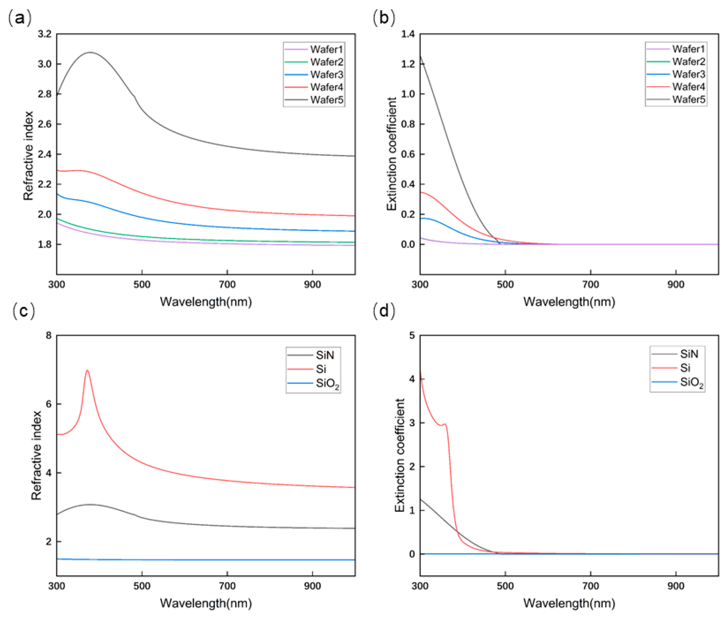
The growth of SiN thin films employs SiH4 and N2 as the reaction gases. The refractive index and extinction coefficient of SiN are primarily influenced by the Si/N atomic ratio. To achieve a higher refractive index in the visible spectrum, the gas flow ratio is set to SiH4:N2 = 55 sccm: 30 sccm, exceeding the normal Si3N4 stoichiometry required for stable chemical bonding between silicon and nitrogen atoms. For the growth of SiO2 dielectric thin films, the reaction gases used are SiH4 and N2O, with a gas flow ratio in the conventional proportions (SiH4:N2O = 20 sccm: 40 sccm). To stabilize the reaction process, 200 sccm of argon gas is introduced into the reaction gas. Detailed deposition parameters are provided in Table 1. A single layer of SiN and SiO2 thin films was deposited on bare Si wafers at 80 °C. The films were measured and characterized using an ellipsometer. The refractive index and extinction coefficient of SiN and SiO2 thin films were numerically fitted using the Cody–Lorentz dispersion model [28] and the Cauchy model [29]. The refractive index and extinction coefficient of Si, SiN, and SiO2 in the visible spectrum are presented in Appendix A.
An optical multilayer film with a single FP cavity was simulated using the Transfer Matrix Method (TMM) model. The SiN (H) layer, with a high refractive index, was designed to be 70 nm thick, while the SiO2 (L) layer, with a low refractive index, remained at 118 nm. The system’s structure was (HL)4 2H L(HL)4, with a central wavelength of 700 nm and four pairs of SiO2/SiN materials on either side of the spacer layer. The DBR structure comprised alternating stacks on both sides of the spacer layer, and the thickness of the intermediate cavity layer material SiN was twice that of 70 nm. The multilayer optical film system was prepared by continuously depositing SiN and SiO2 films at 80 °C using ICPCVD, following modulated SiN and SiO2 film deposition process parameters. The multilayer optical film system was prepared by continuously depositing SiN and SiO2 films at 80 °C using ICPCVD, following modulated SiN and SiO2 film deposition process parameters.

3. Result and Discussion

3.1. Film Thickness Analysis

The 8-inch wafer film prepared by the ICPCVD method is shown in Figure 1a. Four different test points selected randomly on an 8-inch wafer (P1, P2, P3, P4) were tested, respectively, under the incidence of a broad-wavelength light source vertical to the surface, as depicted in Figure 1c. Reflectance spectra analysis indicates that the four tested points exhibit center wavelengths constituting a minimum of 666 nm and a maximum of 692 nm. Peak transmittance achieved included a minimum of 60% and a maximum of 76%. These discrepancies stem from the inhomogeneity of the film deposition. The simulated reflectance spectrum has a center wavelength of 700 nm and a peak transmittance of 94%. The reflectance spectra of the sampled points exhibit a noticeable blueshift in comparison to the design values, accompanied by a reduction in peak transmittance. This deviation may be attributed to measurement errors and scattering losses due to the unevenness of the film surface.
In order to investigate the mismatch between practical thickness and the designed thickness of each layer, a piece of the wafer was cut off from the wafer’s edge for SEM scanning, as depicted in Figure 1b. The SEM image reveals the periodic stacking structure and the spacer layer. Thickness values of each layer were measured from SEM images. For clarity, Table 2 presents both actual and design thickness values for each layer. Furthermore, reflectance spectra for the actual thickness values of each film layer, obtained from SEM images, were re-simulated using the TMM method, as shown in Figure 1c. The results indicate the peak transmittance of the corrected reflectance spectrum at 694 nm is about 90%, and the center wavelength of the reflectance spectrum shifts towards the test spectrum. However, a discrepancy persists between the simulated reflectance spectra of the actual film thicknesses and the measured spectra, possibly attributed to scattering losses arising from uneven film surfaces during testing.
To investigate the influence of potential errors in film thickness on the performance of multilayer films during the deposition process, sample thicknesses were measured, revealing that the error for each layer remained within 15%, as depicted in Table 2. Consequently, the standard deviation for the film thickness error algorithm was set at 0.15, indicating that values could vary by up to a 15% thickness offset. Subsequently, 100 sets of reflectance spectra were calculated, as depicted in Figure 1d. The results indicated a wavelength shift in the center of the reflectance spectra within a range of 7.3 nm, attributable to errors in film layer thickness. The examination of the impact of film thickness errors on wavelength shifts contributes to the assessment of the system’s sensitivity to variations in film thickness. This sensitivity, in turn, serves as an indicator of the stability of an optical element’s performance.

3.2. The Influence of Incident Angle Changes

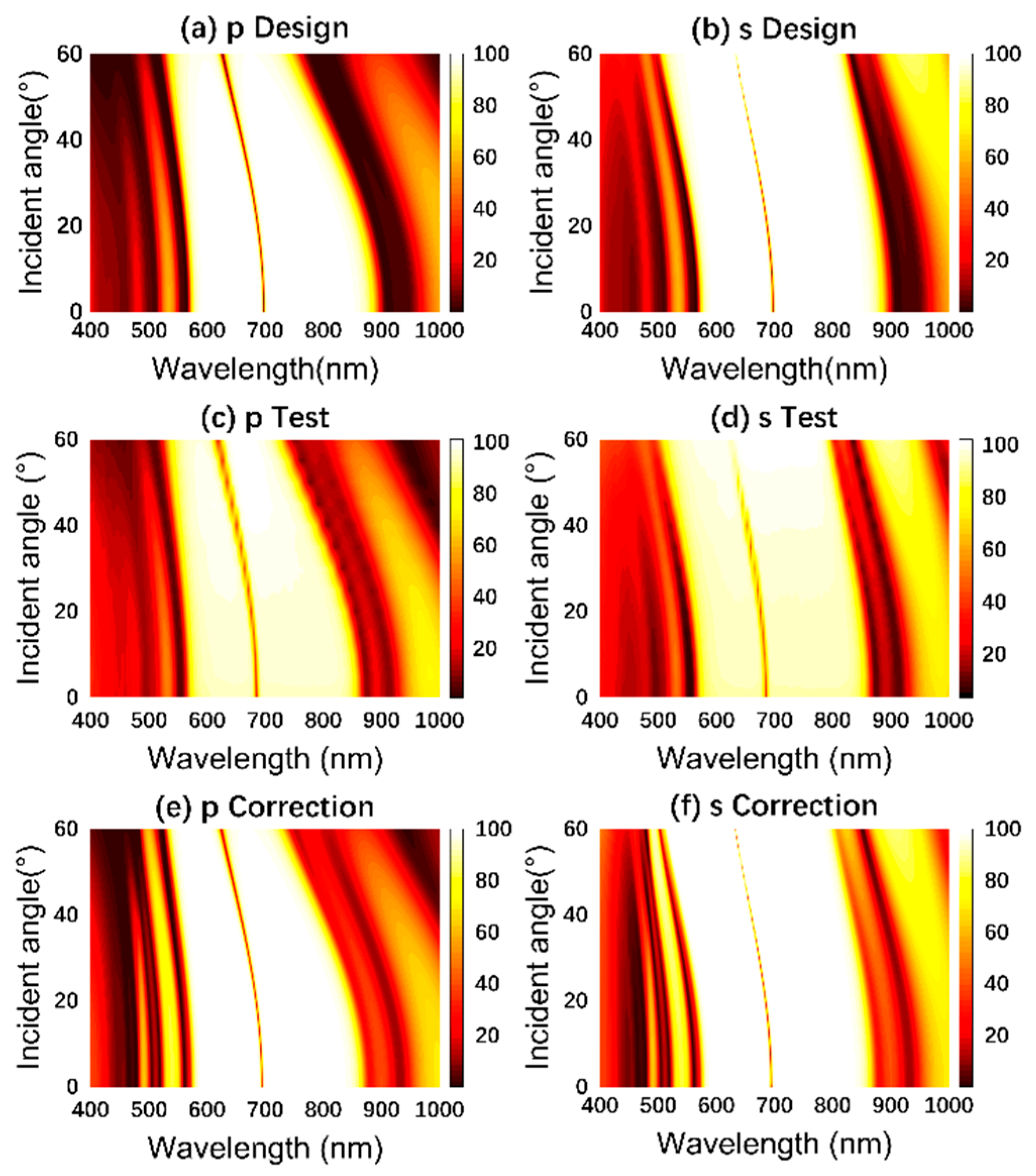
The shift of the cavity mode at different angles of incidence of polarized light was examined by simulating the reflectance spectra of thin films at various angles, as depicted in Figure 2a,b. By placing a film cut from the edge of an 8-inch wafer under p/s polarized light, the reflectance spectra were obtained at various angles of incidence in the wavelength range of 400 nm to 1000 nm. This was achieved using a macro-angle-resolved spectrometer, as illustrated in Figure 2c,d. Additionally, Figure 2e,f displays re-simulated reflectance spectra based on actual film thickness values. These spectra illustrate the correlation between test reflectance spectra and actual film thickness under different angles of p/s polarized light.
Table 3 presents the shift in the center wavelength ( λ 0 ) of the reflection spectrum, indicating a blueshift as the angle of incidence increases and a slight decrease in peak transmittance. Simulated spectra based on theoretical film thickness values deviated from actual measurements, whereas spectra re-simulated with real thickness values aligned more closely with experimental data. This demonstrates that minor thickness discrepancies significantly impact the films’ spectral properties. Hence, precise control over the thickness and uniformity of each layer is crucial during the deposition of multilayer films.

3.3. The Influence of Temperature Changes

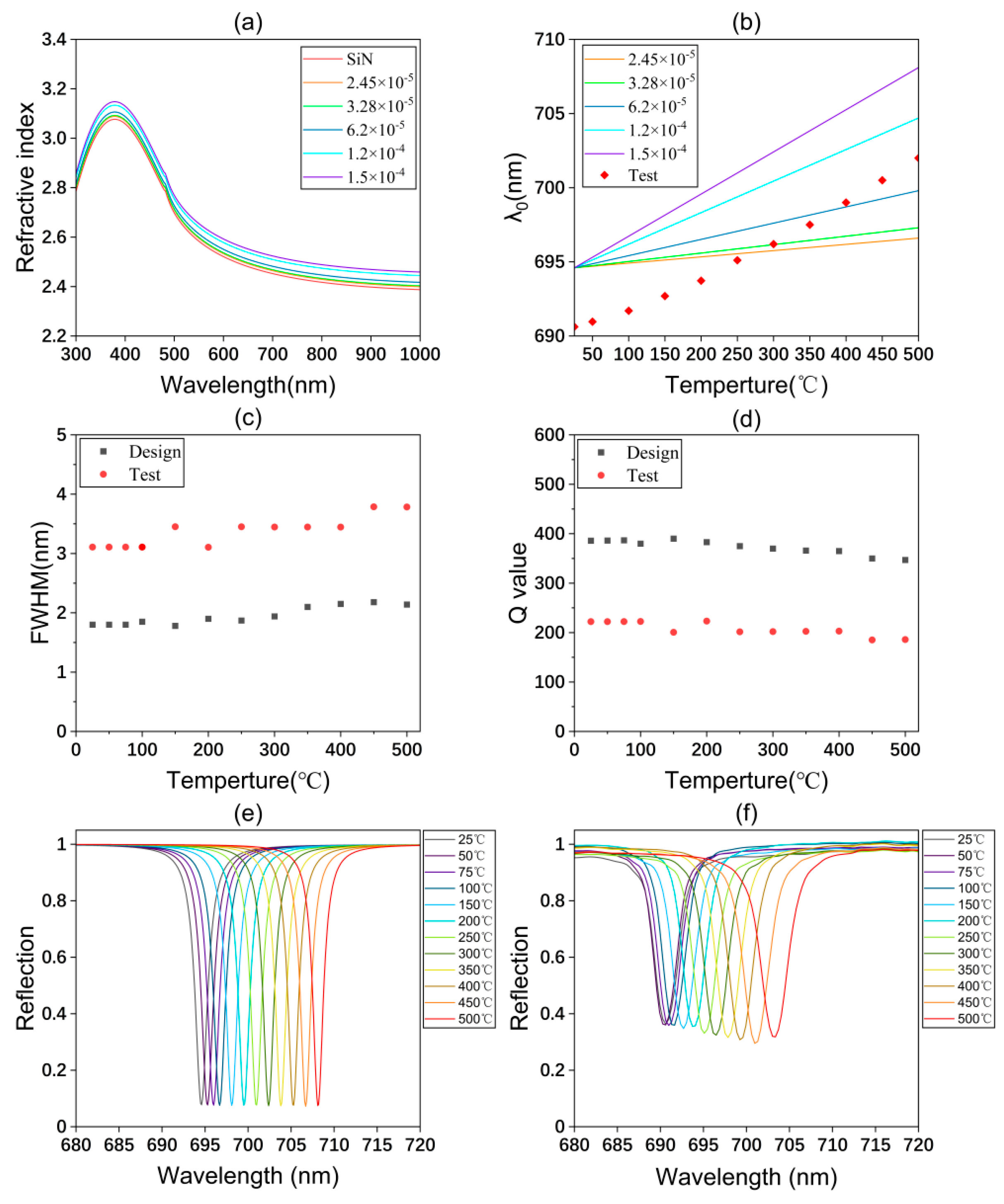
The refractive index values of SiN were calculated using various temperature coefficients, as depicted in Figure 3a. In the simulation, the thickness change in each film layer during the heating process is neglected, as the impact of the linear thermal expansion coefficient is disregarded. The thickness of each film layer is set to its actual measured value. To examine the impact of temperature on the reflective properties of the film, a temperature control device was integrated into the film thickness tester. This device enables a gradual temperature increase from room temperature to 500 °C and temperature stabilization at a specified value. A sample of 2 cm × 2 cm was extracted from the wafer, and reflectance measurements were conducted at 50 °C intervals. The wavelength shift at the center of the reflectance spectrum was measured, reaching 13 nm in the temperature range from room temperature to 500 °C, as illustrated in Figure 3b. This shift was then compared with the simulated wavelength shift using the refractive indices of SiN materials with various temperature coefficients. The magnitude of the center wavelength shift at 1.5 × 10⁻⁴ K−1 for SiN is more in line with the actual test, leading to the initial deduction that the practical temperature coefficient value of the SiN material is approximately 1.5 × 10⁻⁴ K−1.
The quality factor Q is a crucial parameter for assessing the selectivity and precision of the filter film system. In the spectrum, Q is defined as the degree of rectangularization of the passband and the steepness of the transition bands on both sides of the passband. It can be expressed as the ratio between the central wavelength and the full width at half maximum (FWHM), expressed as follows: Q = λ / F W H M . Generally, a higher Q value correlates with a reduced FWHM, leading to enhanced film filtering capabilities. Figure 3c,d show the variation of FWHM and Q with ambient temperature for the designed and tested cavity modes. It is evident that the FWHM slightly increases as the temperature rises, while the Q value shows a slight decrease. The results indicate that an increase in ambient temperature leads to a deterioration in film properties to some extent, highlighting the importance of temperature protection.
In the application of thin-film optical cavities, optimizing the FWHM and maximizing the Q value are crucial parameters for enhancing wavelength selectivity of optical filters and improving sensor sensitivity. A high Q value improves the sharpness of the laser’s resonance peak, resulting in a narrower output spectral line. Figure 3c,d illustrate the changes in the FWHM and Q of the designed and tested cavity modes with ambient temperature. It is evident that the FWHM slightly increases as the temperature rises, while the Q shows a slight decrease. However, it is important to note that, despite significant temperature variations, the changes in FWHM and Q are relatively small. This suggests that the thin-film optical cavity can maintain relatively stable optical properties across different temperatures. Examining the enlarged passband region in Figure 3e,f, the simulated and tested wavelength shifts of the center wavelength in the reflection spectra are 13.4 nm and 13 nm, respectively, when the temperature changes from room temperature to 500 °C. Notably, the simulated and tested wavelength shifts align closely. The thin-film optical cavity exhibits high sensitivity to temperature-induced center wavelength shifts, coupled with its relatively stable optical performance. These characteristics render it unique in the realm of high-resolution and high-precision temperature sensors.

3.4. Chromatic Spatial Characterisation

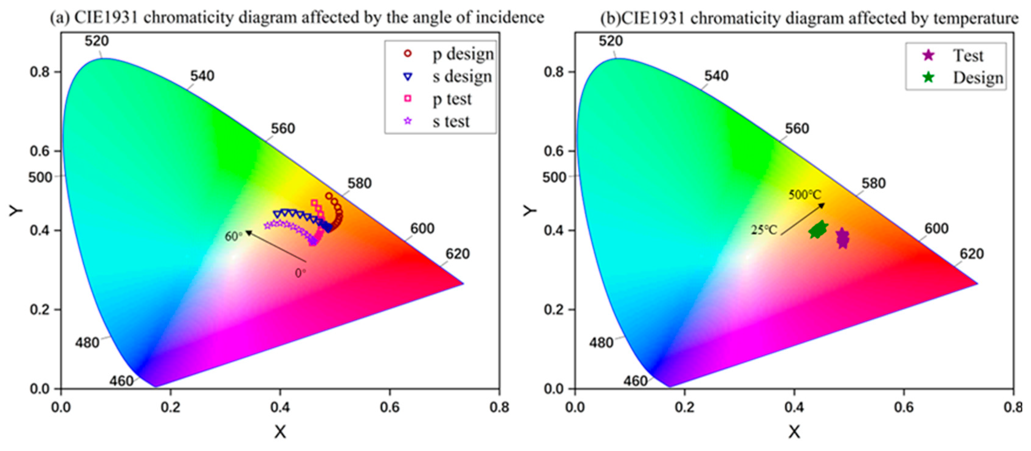
To assess the performance of the prepared films in chromaticity, we plotted the chromaticity coordinates of both experimental and simulated reflectance spectra on a standard CIE 1931 chromaticity diagram. This was performed at various incidence angles and temperatures, as depicted in Figure 4. The results indicate a shift of simulated and designed chromaticity coordinates toward the yellow region with increasing incidence angle. Furthermore, the yellow light saturation and brightness of the film increase gradually as the center wavelength shifts towards the blue. Unlike the angle of incidence, variations in temperature have a negligible impact on the chromaticity coordinates of the film.

4. Conclusions

In conclusion, multilayer films with a single FP cavity were deposited on 8” wafers using ICPCVD at a low temperature of 80 °C. The films were based on SiO2 material and high refractive index SiN material, which were alternately deposited. Simple modulation of the optical performance and large-scale applications can be realized by varying the thickness of the dielectric layer and the manufacturing processes at the wafer level. When irradiated with p/s polarized light waves at variable incident angles, the cavity mode blueshifts with increasing incident angle, and the film maintains the same perceived color. The thin-film optical cavity modes have high sensitivity to ambient temperature sensing and stable optical performance in the temperature interval of 25–500 °C. The results suggest potential applications in CMOS image sensors, displays, and temperature sensors.

Author Contributions

Conceptualization, Y.Z.; methodology, Y.Z. and W.L.; software, Y.Z. and W.L.; validation, Y.Z., Z.G. and J.D.; formal analysis, Y.Z.; investigation, Y.Z., Z.G. and J.D.; data curation, Y.Z.; writing—original draft preparation, Y.Z.; writing—review and editing, Y.Z., W.L., Z.G. and J.D.; supervision, B.L. and C.C.; project administration, B.L. and C.C.; funding acquisition, B.L. and C.C. All authors have read and agreed to the published version of the manuscript.

Funding

We would like to acknowledge the support from the National Key Research and Development Program (no. 2021YFB3202504), the National Key Research and Development Program (no. 2021YFF0704704), and the National Key Research and Development Program (no. 2022YFE0107400).

Institutional Review Board Statement

Not applicable.

Informed Consent Statement

Not applicable.

Data Availability Statement

The data presented in this study are available from the corresponding authors upon reasonable request.

Acknowledgments

Thanks to Xu Cheng for facility maintenance of the ICPCVD system in the 8-inch MEMS line of SITRI in Shanghai. Thanks to Yan Meng at Wuhan Eoptics Corporation (Wuhan, China) for the reflectance spectra measurement for the wafer-scale sample. Thanks to Wang Shan at Shanghai Ideaoptics Corporation (Shanghai, China) for the angle-resolved reflectance spectra measurement with p/s polarization state. Thanks to Shanghai Gatech Corporation (Shanghai, China) for SEM characterization of the cross-section of the multilayer film.

Conflicts of Interest

The authors declare no conflicts of interest.

Appendix A

By modulating the reactive gas flow rate and biasing the RF power to obtain high refractive index SiN films, five sets of SiN film samples were obtained. The optical constants and thicknesses were fitted using the Cody–Lorentz dispersion model for SiN thin-film materials. The refractive indices and extinction coefficients of the five groups of SiN thin-film samples are shown in Figure A1a,b. For the subsequent experiments, we selected the SiN material with the highest refractive index ratio of Si-5. Figure A1c,d shows the refractive indices and extinction coefficients of SiN, SiO2, and substrate Si used in the final experiments.
Figure A1. Refractive index (a) and extinction coefficient (b) of each group of SiN films. Refractive index (c) and extinction coefficient (d) of SiN, Si substrate, and SiO2.
Photonics 11 00329 g0a1

References

  1. Han, J.H.; Kim, D.Y.; Kim, D.; Choi, K.C. Highly Conductive and Flexible Color Filter Electrode Using Multilayer Film Structure. Sci. Rep. 2016, 6, 7. [Google Scholar] [CrossRef] [PubMed]
  2. Li, Z.Y.; Butun, S.; Aydin, K. Large-Area, Lithography-Free Super Absorbers and Color Filters at Visible Frequencies Using Ultrathin Metallic Films. ACS Photonics 2015, 2, 183–188. [Google Scholar] [CrossRef]
  3. Lin, Y.S.; Ho, C.P.; Koh, K.H.; Lee, C. Fabry-Perot Filter Using Grating Structures. Opt. Lett. 2013, 38, 902–904. [Google Scholar] [CrossRef] [PubMed]
  4. Zhai, L.Y.; Xu, J.; Wu, Y.M. Design and Fabrication of Independent-Cavity Fp Tunable Filter. Opt. Commun. 2013, 297, 154–164. [Google Scholar] [CrossRef]
  5. Meng, F.; Yu, H.; Zhou, X.; Wang, M.; Zhang, Y.; Yang, W.; Pan, J. Low Fabrication Cost Wavelength Tunable Wg-Fp Hybrid-Cavity Laser Working over 1.7 Μ M; IOP Publishing Ltd.: Bristol, UK, 2022. [Google Scholar]
  6. Yin, D.; Yu, S.; Fang, Z.; Huang, Q.; Gao, L.; Wang, Z.; Liu, J.; Huang, T.; Zhang, H.; Wang, M.; et al. On-Chip Electro-Optically Tunable Fabry-Perot Cavity Laser on Erbium Doped Thin Film Lithium Niobate. Opt. Mater. Express 2023, 13, 2644–2650. [Google Scholar] [CrossRef]
  7. Chowdhury, H.R.; Han, M. Fiber Optic Temperature Sensor System Using Air-Filled Fabry–Pérot Cavity with Variable Pressure. Sensors 2023, 23, 3302. [Google Scholar] [CrossRef] [PubMed]
  8. Zheng, Y.; Chen, Y.; Zhang, Q.; Tang, Q.; Zhu, Y.; Yu, Y.; Du, C.; Ruan, S. High-Sensitivity Temperature Sensor Based on Fiber Fabry-Pérot Interferometer with UV Glue-Filled Hollow Capillary Fiber. Sensors 2023, 23, 7687. [Google Scholar] [CrossRef] [PubMed]
  9. Tang, S.; Zou, M.; Zhao, C.; Jiang, Y.; Chen, R.; Xu, Z.; Yang, C.; Wang, X.; Dong, B.; Wang, Y.; et al. Fabry-Perot Interferometer Based on a Fiber-Tip Fixed-Supported Bridge for Fast Glucose Concentration Measurement. Biosensors 2022, 12, 391. [Google Scholar] [CrossRef] [PubMed]
  10. Dai, J.; Gao, W.; Liu, B.; Cao, X.; Tao, T.; Xie, Z.; Zhao, H.; Chen, D.; Ping, H.; Zhang, R. Design and Fabrication of UV Band-Pass Filters Based on SiO2/Si3N4 Dielectric Distributed Bragg Reflectors. Appl. Surf. Sci. 2016, 364, 886–891. [Google Scholar] [CrossRef]
  11. Ailing, Z.; Heliang, L.; Demokan, M.S.; Tam, H.Y. Stable and Broad Bandwidth Multiwavelength Fiber Ring Laser Incorporating a Highly Nonlinear Photonic Crystal Fiber. IEEE Photonics Technol. Lett. 2005, 17, 2535–2537. [Google Scholar] [CrossRef]
  12. Chen, H.; Liang, Y. Analysis of the Tunable Asymmetric Fiber F-P Cavity for Fiber Strain Sensor Edge-Filter Demodulation. Photonic Sens. 2014, 4, 338–343. [Google Scholar] [CrossRef]
  13. Lee, J.W.; Mackenzie, K.D.; Johnson, D.; Sasserath, J.N.; Pearton, S.J.; Ren, F. Low Temperature Silicon Nitride and Silicon Dioxide Film Processing by Inductively Coupled Plasma Chemical Vapor Deposition. J. Electrochem. Soc. 2000, 147, 1481–1486. [Google Scholar] [CrossRef]
  14. Shi, M.; Shao, X.M.; Tang, H.J.; Li, T.; Wang, Y.J.; Li, X.; Gong, H.M. Inductively Coupled Plasma Chemical Vapor Deposition Silicon Nitride for Passivation of In0.83Ga0.17As Photodiodes. Infrared Phys. Technol. 2014, 67, 197–201. [Google Scholar] [CrossRef]
  15. Macleod, H.A. Thin-Film Optical Filters; Institute of Physics Pub.: Bristol, UK, 2001. [Google Scholar]
  16. Habermehl, S. Coefficient of Thermal Expansion and Biaxial Young’s Modulus in Si-Rich Silicon Nitride Thin Films. J. Vac. Sci. Technol. A 2018, 36, 8. [Google Scholar] [CrossRef]
  17. Hu, D.; Huang, Q.a.; Li, W. Structure for Electrical Measurement of the Thermal Expansion Coefficient of Polysilicon Thin Films. Chin. J. Semicond. 2008, 29, 2018–2022. [Google Scholar]
  18. Tada, H.; Kumpel, A.E.; Lathrop, R.E.; Slanina, J.B.; Nieva, P.; Zavracky, P.; Miaoulis, I.N.; Wong, P.Y. Thermal Expansion Coefficient of Polycrystalline Silicon and Silicon Dioxide Thin Films at High Temperatures. J. Appl. Phys. 2000, 87, 4189–4193. [Google Scholar] [CrossRef]
  19. Arbabi, A.; Goddard, L.L. Measurements of the Refractive Indices and Thermo-Optic Coefficients of Si3N4 and SiOx Using Microring Resonances. Opt. Lett. 2013, 38, 3878–3881. [Google Scholar] [CrossRef]
  20. Li, B.; Zhang, S.; Xie, P.; Zhang, L.; Liu, D.; Zhang, F. Improving Low-Temperature Performance of Infrared Thin-Film Interference Filters Utilizing Temperature Dependence of Refractive Index of Pb1−xGexTe. In Proceedings of the Conference on Infrared Components and Their Applications, Beijing, China, 8–11 November 2004. [Google Scholar]
  21. Yang, X.Y.; Li, H.; You, L.X.; Zhang, W.J.; Zhang, L.; Wang, Z.; Xie, X.M. Temperature Dependence of an Optical Narrow-Bandpass Filter at 1.5 μm. Appl. Opt. 2015, 54, 96–100. [Google Scholar] [CrossRef] [PubMed]
  22. Palik, E.D. (Ed.) Chapter 3—Thermo-Optic Coefficients. In Handbook of Optical Constants of Solids; Academic Press: Burlington, MA, USA, 1997; pp. 115–261. [Google Scholar]
  23. Mondal, P.; Venkatachalam, P.; Singh, R.; Shelwade, S.; Sushma, G.; Selvaraja, S.K. Linear and Nonlinear Characterization of a Broadband Integrated Si-Rich Silicon Nitride Racetrack Ring Resonator for on-Chip Applications. Appl. Opt. 2023, 62, 3703–3709. [Google Scholar] [CrossRef]
  24. Zanatta, A.R.; Gallo, I.B. The Thermo Optic Coefficient of Amorphous SiN Films in the near-Infrared and Visible Regions and Its Experimental Determination. Appl. Phys. Express 2013, 6, 4. [Google Scholar] [CrossRef]
  25. Pruiti, N.G.; Klitis, C.; Gough, C.; May, S.; Sorel, M. Thermo-Optic Coefficient of PECVD Silicon-Rich Silicon Nitride. Opt. Lett. 2020, 45, 6242–6245. [Google Scholar] [CrossRef] [PubMed]
  26. Broadbent, A.D. A Critical Review of the Development of the CIE1931 RGB Color-Matching Functions. Color Res. Appl. 2004, 29, 267–272. [Google Scholar] [CrossRef]
  27. Smith, T.; Guild, J. The CIE Colorimetric Standards and Their Use. Trans. Opt. Soc. 1931, 33, 73. [Google Scholar] [CrossRef]
  28. Price, J.; Hung, P.Y.; Rhoad, T.; Foran, B.; Diebold, A.C. Spectroscopic Ellipsometry Characterization of HfxSiyOz Films Using the Cody-Lorentz Parameterized Model. Appl. Phys. Lett. 2004, 85, 1701–1703. [Google Scholar] [CrossRef]
  29. Zhang, P.; Li, C.; Zhang, M.; Chen, T.; Wang, D.S. Optical Constants of Thin Films of Silicon Oxycarbide Using the Transmission Spectrum. Spectr. Lett. 2015, 48, 367–370. [Google Scholar]
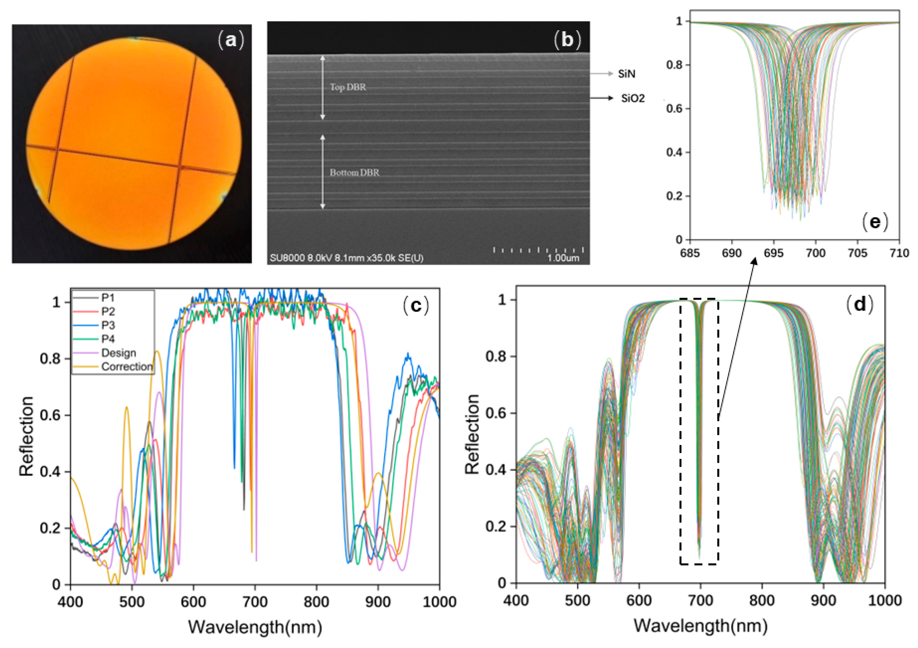
Figure 1. (a) Photograph of the fabricated sample, an 8″ class wafer filter. (b) Scanning electron microscope (SEM) image of the cross-section of the fabricated filter. (c) The reflectance spectra of four randomly sampled points on the film filter, the simulated reflectance spectrum of the designed structure, and the reflectance spectrum by simulation with actual film thickness obtained from SEM image. (d) Hundred sets of reflectance spectra of films with different thickness errors. (e) Magnified view of cavity mold spectrum.
Photonics 11 00329 g001
Figure 2. Reflectance spectra were measured in (a) p-polarization and (b) s-polarization. Reflectance spectra were simulated at (c) p-polarization and (d) s-polarization based on the designed film thickness values. Simulated reflectance spectra with actual film thickness values for (e) p-polarization and (f) s-polarization.
Photonics 11 00329 g002
Figure 3. Refractive index values of SiN material for different temperature coefficients (a) and the temperature-induced shifts of simulated and measured cavity modes (b); variations in the designed and measured cavity mode full width at half maximum (FWHM) (c) and Q-values (d) with changes in environmental temperature; and the simulated (e) and measured (f) shifts of cavity modes within the multilayer film system as a function of environmental temperature.
Photonics 11 00329 g003
Figure 4. (a) CIE 1931 chromaticity diagram showing the color coordinates of the film in the chromaticity diagram as the incident angle varies from 0° to 60°. (b) Depiction of the color coordinates of the film on the chromaticity diagram as the environmental temperature changes from 25 °C to 500 °C.
Photonics 11 00329 g004
Table 1. Deposition parameters of SiN and SiO2 single layer grown by ICPCVD.
Deposition MaterialSiNSiO2
SiH4 gas flow/cm3 min−15520
N2 gas flow/cm3 min−1300
N2O gas flow/cm3 min−1040
Ar gas flow/cm3 min−1200200
Reaction pressure/mTorr1616
Reaction temperature/°C8080
RF power/W300300
Table 2. Film thickness values of each layer under simulation and fabrication.
No. of LayersMaterials
(from Top to Bottom)
Simulation
Thickness (nm)
Fabrication Thickness (nm)Percentage Deviation
1SiN/SiO270/11881/102+15.7%/−13.6%
2SiN/SiO270/11881/109+15.7%/−7.6%
3SiN/SiO270/118178/106+11.4%/−10.2%
4SiN/SiO270/11878/107+11.4%/−9.3%
5SiN/SiO2140/118148/107+5.7%/−9.3%
6SiN/SiO270/11877/101+10%/−14.4%
7SiN/SiO270/11879/102+12.8%/−13.6%
8SiN/SiO270/11878/108+11.4%/−8.4%
9SiN/SiO270/11878/104+11.4%/−11.8%
Note: The layer furthest from the Si substrate is the first layer.
Table 3. The central wavelength and transmittance peak of p/s-polarized spectra at different angles.
Reflection SpectraPolarization λ 0 (nm)Transmission Peak
40°40°
Measured spectrap68565070.6%62.4%
s68565270.6%61.7%
Simulated spectra of the designed structurep69866593.1%91%
s69866493.1%90.3%
Simulated spectra with actual thicknessp69066589.1%73.1%
s69065889.1%71.4%
Disclaimer/Publisher’s Note: The statements, opinions and data contained in all publications are solely those of the individual author(s) and contributor(s) and not of MDPI and/or the editor(s). MDPI and/or the editor(s) disclaim responsibility for any injury to people or property resulting from any ideas, methods, instructions or products referred to in the content.