Design and Optimization of Silver Nanostructured Arrays in Plasmonic Metamaterials for Sensitive Imaging Applications

 , , and
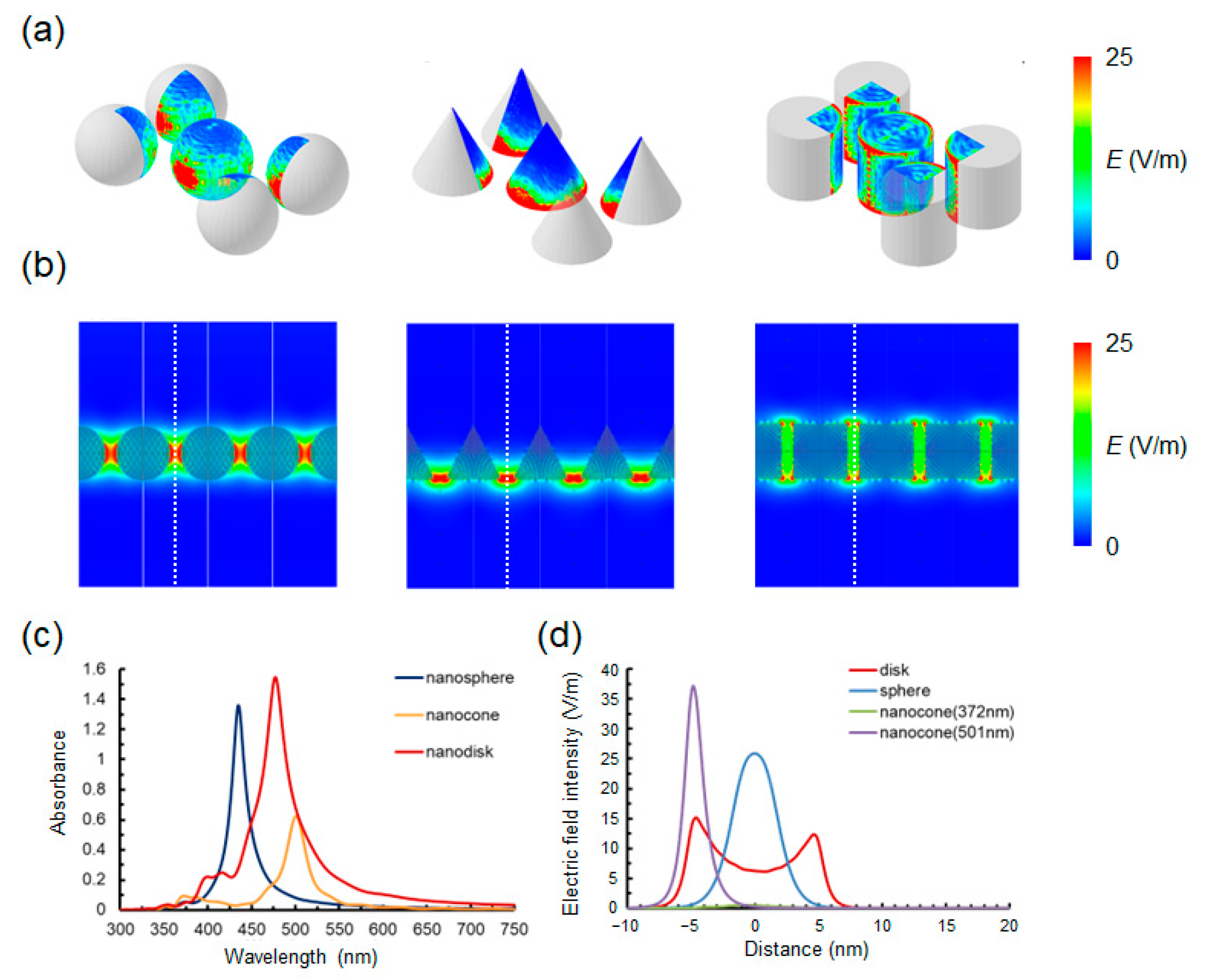
Abstract
1. Introduction
2. Methods
3. Results and Discussions
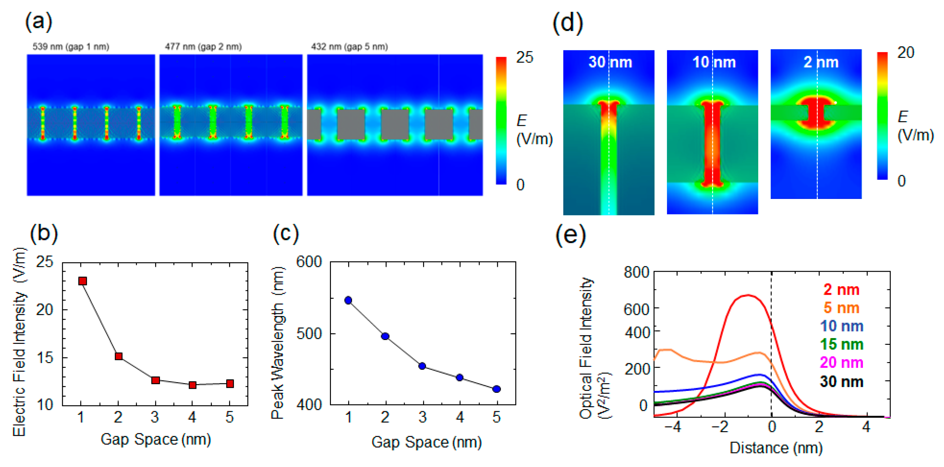
3.1. Nanostructure Geometries for Optimal Electric Field Localization
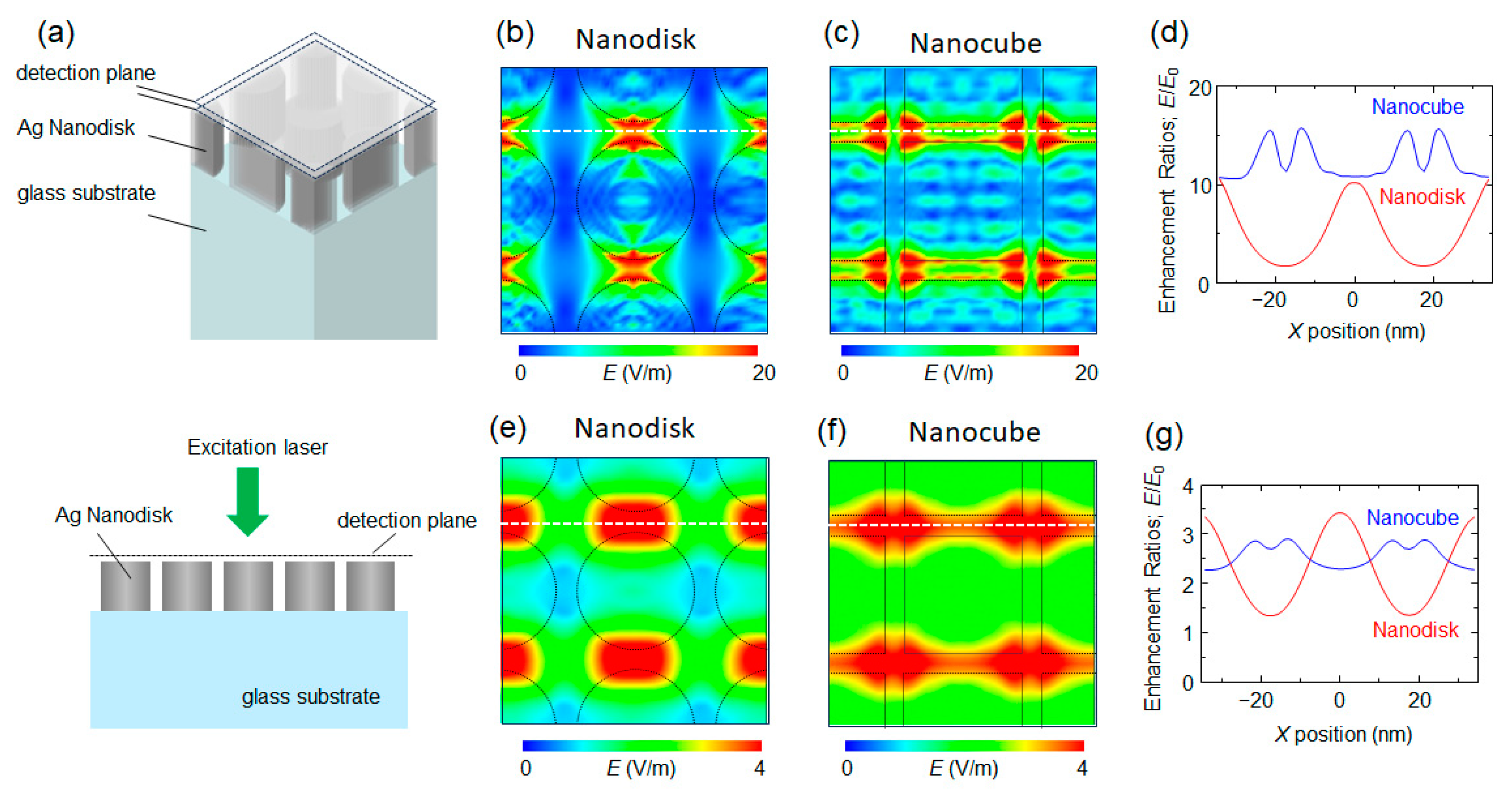
3.2. Optimization of Two-Dimensional Nano-Array Structures
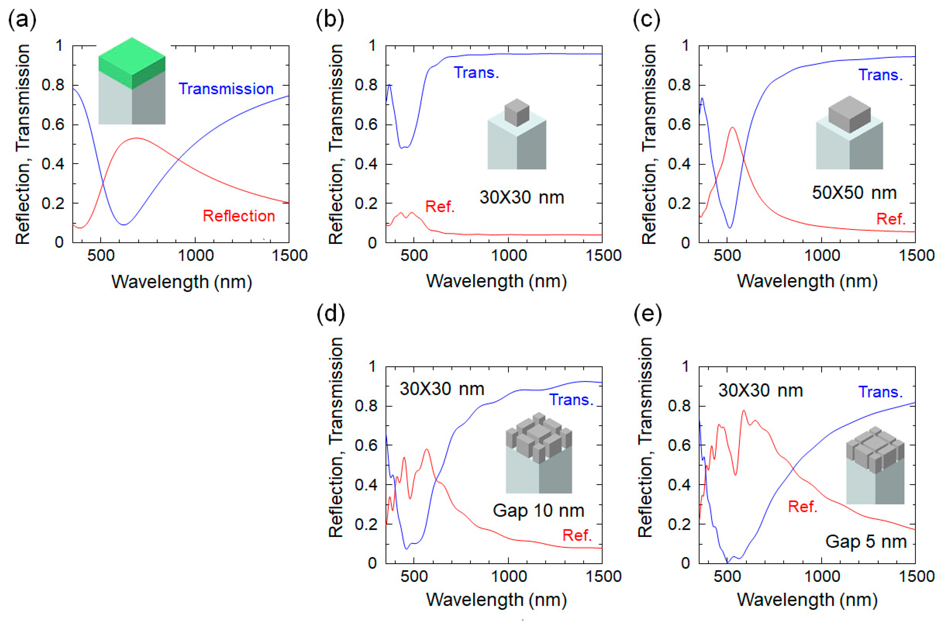
3.3. Plasmonic Metamaterials Using MIM Structures with Nanocube Arrays
4. Conclusions
Author Contributions
Funding
Institutional Review Board Statement
Informed Consent Statement
Data Availability Statement
Conflicts of Interest
References
- Yao, K.; Liu, Y. Plasmonic metamaterials. Nanotechnol. Rev. 2014, 3, 177–210. [Google Scholar] [CrossRef]
- Tang, S.; He, Q.; Xiao, S.; Huang, X.; Zhou, L. Fractal plasmonic metamaterials: Physics and applications. Nanotechnol. Rev. 2015, 4, 277–288. [Google Scholar] [CrossRef]
- Hess, O.; Pendry, J.B.; Maier, S.A.; Oulton, R.F.; Hamm, J.M.; Tsakmakidis, K.L. Active nanoplasmonic metamaterials. Nat. Mater. 2012, 11, 573–584. [Google Scholar] [CrossRef]
- Cui, Y.; He, Y.; Jin, Y.; Ding, F.; Yang, L.; Ye, Y.; Zhong, S.; Lin, Y.; He, S. Plasmonic and metamaterial structures as electromagnetic absorbers. Laser Photonics Rev. 2014, 8, 495–520. [Google Scholar] [CrossRef]
- Shin, H.; Fan, S. All-angle negative refraction for surface plasmon waves using a metal-dielectric-metal structure. Phys. Rev. Lett. 2006, 96, 073907. [Google Scholar] [CrossRef]
- Xu, T.; Agrawal, A.; Abashin, M.; Chau, K.J.; Lezec, H.J. All-angle negative refraction and active flat lensing of ultraviolet light. Nature 2013, 497, 470–474. [Google Scholar] [CrossRef]
- Su, D.; Zhang, X.-Y.; Ma, Y.-L.; Shan, F.; Wu, J.-Y.; Fu, X.-C.; Zhang, L.-J.; Yuan, K.-Q.; Zhang, T. Real-Time Electro-Optical Tunable Hyperlens under Subwavelength Scale. IEEE Photonics J. 2018, 10, 1–9. [Google Scholar] [CrossRef]
- Luo, X. Subwavelength Artificial Structures: Opening a New Era for Engineering Optics. Adv. Mater. 2019, 31, e18046802019. [Google Scholar] [CrossRef]
- Cheng, B.H.; Ho, Y.Z.; Lan, Y.C.; Tsai, D.P. Optical Hybrid-Superlens Hyperlens for Superresolution Imaging. IEEE J. Sel. Top. Quantum Electron. 2013, 19, 4601305. [Google Scholar] [CrossRef]
- Silveirinha, M.G.; Alu, A.; Engheta, N. Parallel-plate metamaterials for cloaking structures. Phys. Rev. E Stat. Nonlinear Soft Matter Phys. 2007, 75, 036603. [Google Scholar] [CrossRef]
- Monticone, F.; Alù, A. Metamaterials and plasmonics: From nanoparticles to nanoantenna arrays, metasurfaces, and metamaterials. Chin. Phys. B 2014, 23, 047809. [Google Scholar] [CrossRef]
- Alù, A.; Engheta, N. Cloaking a receiving antenna or a sensor with plasmonic metamaterials. Metamaterials 2010, 4, 153–159. [Google Scholar] [CrossRef]
- Ogawa, S.; Kimata, M. Metal-Insulator-Metal-Based Plasmonic Metamaterial Absorbers at Visible and Infrared Wavelengths: A Review. Materials 2018, 11, 458. [Google Scholar] [CrossRef]
- Li, J.; Gan, R.; Guo, Q.; Liu, H.; Xu, J.; Yi, F. Tailoring optical responses of infrared plasmonic metamaterial absorbers by optical phonons. Opt. Express 2018, 26, 16769–16781. [Google Scholar] [CrossRef]
- Lai, G.; Liang, R.; Zhang, Y.; Bian, Z.; Yi, L.; Zhan, G.; Zhao, R. Double plasmonic nanodisks design for electromagnetically induced transparency and slow light. Opt. Express 2015, 23, 6554–6561. [Google Scholar] [CrossRef]
- Bai, Z.; Huang, G.; Liu, L.; Zhang, S. Giant Kerr nonlinearity and low-power gigahertz solitons via plasmon-induced transparency. Sci. Rep. 2015, 5, 13780. [Google Scholar] [CrossRef]
- Pang, S.; Huo, Y.; Xie, Y.; Hao, L. Fano resonance in MIM waveguide structure with oblique rectangular cavity and its application in sensor. Opt. Commun. 2016, 381, 409–413. [Google Scholar] [CrossRef]
- Huang, W.; Xu, R.; Lin, Y.-S.; Chen, C.-H. Three-dimensional pyramid metamaterial with tunable broad absorption bandwidth. AIP Adv. 2020, 10, 035125. [Google Scholar] [CrossRef]
- Chorsi, H.T.; Lee, Y.; Alu, A.; Zhang, J.X.J. Tunable plasmonic substrates with ultrahigh Q-factor resonances. Sci. Rep. 2017, 7, 15985. [Google Scholar] [CrossRef]
- Luo, X.; Pu, M.; Guo, Y.; Li, X.; Zhang, F.; Ma, X. Catenary Functions Meet Electromagnetic Waves: Opportunities and Promises. Adv. Opt. Mater. 2020, 8, 2001194. [Google Scholar] [CrossRef]
- Ma, C. Designing super-resolution metalenses by the combination of metamaterials and nanoscale plasmonic waveguide couplers. J. Nanophotonics 2011, 5, 051604. [Google Scholar] [CrossRef]
- Ogawa, S.; Kimata, M. Wavelength- or Polarization-Selective Thermal Infrared Detectors for Multi-Color or Polarimetric Imaging Using Plasmonics and Metamaterials. Materials 2017, 10, 493. [Google Scholar] [CrossRef]
- Wan, W.; Gao, J.; Yang, X. Metasurface Holograms for Holographic Imaging. Adv. Opt. Mater. 2017, 5, 1700541. [Google Scholar] [CrossRef]
- Nagasaki, Y.; Hotta, I.; Suzuki, M.; Takahara, J. Metal-Masked Mie-Resonant Full-Color Printing for Achieving Free-Space Resolution Limit. ACS Photonics 2018, 5, 3849–3855. [Google Scholar] [CrossRef]
- Mudachathi, R.; Tanaka, T. Up Scalable Full Colour Plasmonic Pixels with Controllable Hue, Brightness and Saturation. Sci. Rep. 2017, 7, 1199. [Google Scholar] [CrossRef]
- Cheng, F.; Gao, J.; Stan, L.; Rosenmann, D.; Czaplewski, D.; Yang, X. Aluminum plasmonic metamaterials for structural color printing. Opt. Express 2015, 23, 14552–14560. [Google Scholar] [CrossRef]
- Cheng, F.; Yang, X.; Rosenmann, D.; Stan, L.; Czaplewski, D.; Gao, J. Enhanced structural color generation in aluminum metamaterials coated with a thin polymer layer. Opt. Express 2015, 23, 25329–25339. [Google Scholar] [CrossRef]
- Deshpande, R.A.; Roberts, A.S.; Bozhevolnyi, S.I. Plasmonic color printing based on third-order gap surface plasmons [Invited]. Opt. Mater. Express 2019, 9, 717. [Google Scholar] [CrossRef]
- Keshavarz Hedayati, M.; Elbahri, M. Review of Metasurface Plasmonic Structural Color. Plasmonics 2016, 12, 1463–1479. [Google Scholar] [CrossRef]
- Wang, J.; Xu, Z.; Kotsifaki, D.G. Plasmonic and metamaterial biosensors: A game-changer for virus detection. Sens. Diagn. 2023, 2, 600–619. [Google Scholar] [CrossRef]
- Wang, Z.; Chen, J.; Khan, S.A.; Li, F.; Shen, J.; Duan, Q.; Liu, X.; Zhu, J. Plasmonic Metasurfaces for Medical Diagnosis Applications: A Review. Sensors 2021, 22, 133. [Google Scholar] [CrossRef]
- Kabashin, A.V.; Evans, P.; Pastkovsky, S.; Hendren, W.; Wurtz, G.A.; Atkinson, R.; Pollard, R.; Podolskiy, V.A.; Zayats, A.V. Plasmonic nanorod metamaterials for biosensing. Nat. Mater. 2009, 8, 867–871. [Google Scholar] [CrossRef]
- Kravets, V.G.; Schedin, F.; Jalil, R.; Britnell, L.; Gorbachev, R.V.; Ansell, D.; Thackray, B.; Novoselov, K.S.; Geim, A.K.; Kabashin, A.V.; et al. Singular phase nano-optics in plasmonic metamaterials for label-free single-molecule detection. Nat. Mater. 2013, 12, 304–309. [Google Scholar] [CrossRef]
- Politano, G.G.; Cazzanelli, E.; Versace, C.; Vena, C.; De Santo, M.P.; Castriota, M.; Ciuchi, F.; Bartolino, R. Graphene oxide on magnetron sputtered silver thin films for SERS and metamaterial applications. Appl. Surf. Sci. 2018, 427, 927–933. [Google Scholar] [CrossRef]
- Wang, K.; Qiu, Z.; Qin, Y.; Feng, L.; Huang, L.; Xiao, G. Preparation and SERS performance of silver nanowires arrays on paper by automatic writing method. Spectrochim. Acta A Mol. Biomol. Spectrosc. 2022, 281, 121580. [Google Scholar] [CrossRef]
- Borchers, A.; Pieler, T. Programming pluripotent precursor cells derived from Xenopus embryos to generate specific tissues and organs. Genes 2010, 1, 413–426. [Google Scholar] [CrossRef]
- Sayed, S.I.; Mahmoud, K.R.; Mubarak, R.I. Design and optimization of broadband metamaterial absorber based on manganese for visible applications. Sci. Rep. 2023, 13, 11937. [Google Scholar] [CrossRef]
- Ji, W.; Chang, J.; Xu, H.X.; Gao, J.R.; Groblacher, S.; Urbach, H.P.; Adam, A.J.L. Recent advances in metasurface design and quantum optics applications with machine learning, physics-informed neural networks, and topology optimization methods. Light Sci. Appl. 2023, 12, 169. [Google Scholar] [CrossRef]
- Lan, G.; Wang, Y.; Ou, J.Y. Optimization of metamaterials and metamaterial-microcavity based on deep neural networks. Nanoscale Adv. 2022, 4, 5137–5143. [Google Scholar] [CrossRef]
- Okamoto, K.; Lin, B.; Imazu, K.; Yoshida, A.; Toma, K.; Toma, M.; Tamada, K. Tuning Colors of Silver Nanoparticle Sheets by Multilayered Crystalline Structures on Metal Substrates. Plasmonics 2012, 8, 581–590. [Google Scholar] [CrossRef]
- Okamoto, K.; Tanaka, D.; Degawa, R.; Li, X.; Wang, P.; Ryuzaki, S.; Tamada, K. Electromagnetically induced transparency of a plasmonic metamaterial light absorber based on multilayered metallic nanoparticle sheets. Sci. Rep. 2016, 6, 36165. [Google Scholar] [CrossRef]
- Shinohara, S.; Tanaka, D.; Okamoto, K.; Tamada, K. Colorimetric plasmon sensors with multilayered metallic nanoparticle sheets. Phys. Chem. Chem. Phys. 2015, 17, 18606–18612. [Google Scholar] [CrossRef]
- Degawa, R.; Wang, P.; Tanaka, D.; Park, S.; Sakai, N.; Tatsuma, T.; Okamoto, K.; Tamada, K. Colorimetric Detection of an Airborne Remote Photocatalytic Reaction Using a Stratified Ag Nanoparticle Sheet. Langmuir 2016, 32, 8154–8162. [Google Scholar] [CrossRef]
- Ishijima, A.; Wang, P.; Ryuzaki, S.; Okamoto, K.; Tamada, K. Comparison of LSPR-mediated enhanced fluorescence excited by S- and P-polarized light on a two-dimensionally assembled silver nanoparticle sheet. Appl. Phys. Lett. 2018, 113, 171602. [Google Scholar] [CrossRef]
- Masuda, S.; Yanase, Y.; Usukura, E.; Ryuzaki, S.; Wang, P.P.; Okamoto, K.; Kuboki, T.; Kidoaki, S.; Tamada, K. High-resolution imaging of a cellattached nanointerface using a gold-nanoparticle two-dimensional sheet. Sci. Rep. 2017, 7, 3720. [Google Scholar] [CrossRef]
- Calandrini, E.; Cerea, A.; De Angelis, F.; Zaccaria, R.P.; Toma, A. Magnetic hot-spot generation at optical frequencies: From plasmonic metamolecules to all-dielectric nanoclusters. Nanophotonics 2018, 8, 45–62. [Google Scholar] [CrossRef]
- Su, D.S.; Tsai, D.P.; Yen, T.J.; Tanaka, T. Ultrasensitive and Selective Gas Sensor Based on a Channel Plasmonic Structure with an Enormous Hot Spot Region. ACS Sens. 2019, 4, 2900–2907. [Google Scholar] [CrossRef]
- Wy, Y.; Jung, H.; Hong, J.W.; Han, S.W. Exploiting Plasmonic Hot Spots in Au-Based Nanostructures for Sensing and Photocatalysis. Acc. Chem. Res. 2022, 55, 831–843. [Google Scholar] [CrossRef]
- Johnson, P.B.; Christy, R.W. Optical Constants of the Noble Metals. Phys. Rev. B 1972, 6, 4370–4379. [Google Scholar] [CrossRef]
- Bishop, K.J.; Wilmer, C.E.; Soh, S.; Grzybowski, B.A. Nanoscale forces and their uses in self-assembly. Small 2009, 5, 1600–1630. [Google Scholar] [CrossRef]
- Cheng, S.-C.; Wen, T.-C. Robust SERS substrates with massive nanogaps derived from silver nanocubes self-assembled on massed silver mirror via 1,2-ethanedithiol monolayer as linkage and ultra-thin spacer. Mater. Chem. Phys. 2014, 143, 1331–1337. [Google Scholar] [CrossRef]
- Fan, J.A.; Wu, C.H.; Bao, K.; Bao, J.M.; Bardhan, R.; Halas, N.J.; Manoharan, V.N.; Nordlander, P.; Shvets, G.; Capasso, F. Self-Assembled Plasmonic Nanoparticle Clusters. Science 2010, 328, 1135–1138. [Google Scholar] [CrossRef]
- Gong, J.; Li, G.; Tang, Z. Self-assembly of noble metal nanocrystals: Fabrication, optical property, and application. Nano Today 2012, 7, 564–585. [Google Scholar] [CrossRef]
- Hanske, C.; Tebbe, M.; Kuttner, C.; Bieber, V.; Tsukruk, V.V.; Chanana, M.; Konig, T.A.; Fery, A. Strongly coupled plasmonic modes on macroscopic areas via template-assisted colloidal self-assembly. Nano Lett. 2014, 14, 6863–6871. [Google Scholar] [CrossRef]
- Rozin, M.J.; Rosen, D.A.; Dill, T.J.; Tao, A.R. Colloidal metasurfaces displaying near-ideal and tunable light absorbance in the infrared. Nat. Commun. 2015, 6, 7325. [Google Scholar] [CrossRef]
- Wang, Y.; Zheng, Y.; Huang, C.Z.; Xia, Y. Synthesis of Ag nanocubes 18-32 nm in edge length: The effects of polyol on reduction kinetics, size control, and reproducibility. J. Am. Chem. Soc. 2013, 135, 1941–1951. [Google Scholar] [CrossRef]
- Zhang, Q.; Li, W.; Wen, L.P.; Chen, J.; Xia, Y. Facile synthesis of Ag nanocubes of 30 to 70 nm in edge length with CF(3)COOAg as a precursor. Chemistry 2010, 16, 10234–10239. [Google Scholar] [CrossRef]
- Zhou, S.; Li, J.; Gilroy, K.D.; Tao, J.; Zhu, C.; Yang, X.; Sun, X.; Xia, Y. Facile Synthesis of Silver Nanocubes with Sharp Corners and Edges in an Aqueous Solution. ACS Nano 2016, 10, 9861–9870. [Google Scholar] [CrossRef]
- Mitomo, H.; Takeuchi, C.; Sugiyama, R.; Tamada, K.; Ijiro, K. Thermo-Responsive Silver Nanocube Assembled Films. Bull. Chem. Soc. Jpn. 2022, 95, 771–773. [Google Scholar] [CrossRef]
- Okamoto, K.; Okura, K.; Wang, P.; Ryuzaki, S.; Tamada, K. Flexibly tunable surface plasmon resonance by strong mode coupling using a random metal nanohemisphere on mirror. Nanophotonics 2020, 9, 3409–3418. [Google Scholar] [CrossRef]
- Shimanoe, K.; Endo, S.; Matsuyama, T.; Wada, K.; Okamoto, K. Localized surface plasmon resonance in deep ultraviolet region below 200 nm using a nanohemisphere on mirror structure. Sci. Rep. 2021, 11, 5169. [Google Scholar] [CrossRef]
- Shimanoe, K.; Endo, S.; Matsuyama, T.; Wada, K.; Okamoto, K. Metallic nanovoid and nano hemisphere structures fabricated via simple methods to control localized surface plasmon resonances in UV and near IR wavelength regions. Appl. Phys. Express 2021, 14, 042007. [Google Scholar] [CrossRef]
- Wan, M.; Zhai, W.; Song, Y.; Li, Y.; Ji, P.; Zhou, F. Actively controllable EIT-like resonance between localized and propagating surface plasmons for optical switching. J. Mod. Opt. 2015, 62, 1264–1269. [Google Scholar] [CrossRef]
- Yang, J.; Sun, Q.; Ueno, K.; Shi, X.; Oshikiri, T.; Misawa, H.; Gong, Q. Manipulation of the dephasing time by strong coupling between localized and propagating surface plasmon modes. Nat. Commun. 2018, 9, 4858. [Google Scholar] [CrossRef]
- Huang, Y.; Ma, L.; Li, J.; Zhang, Z. Nanoparticle-on-mirror cavity modes for huge and/or tunable plasmonic field enhancement. Nanotechnology 2017, 28, 105203. [Google Scholar] [CrossRef]
- Zhang, C.; Hugonin, J.-P.; Greffet, J.-J.; Sauvan, C. Surface Plasmon Polaritons Emission with Nanopatch Antennas: Enhancement by Means of Mode Hybridization. ACS Photonics 2019, 6, 2788–2796. [Google Scholar] [CrossRef]
- Shi, X.; Ueno, K.; Oshikiri, T.; Sun, Q.; Sasaki, K.; Misawa, H. Enhanced water splitting under modal strong coupling conditions. Nat. Nanotechnol. 2018, 13, 953–958. [Google Scholar] [CrossRef]


Disclaimer/Publisher’s Note: The statements, opinions and data contained in all publications are solely those of the individual author(s) and contributor(s) and not of MDPI and/or the editor(s). MDPI and/or the editor(s) disclaim responsibility for any injury to people or property resulting from any ideas, methods, instructions or products referred to in the content. |
© 2024 by the authors. Licensee MDPI, Basel, Switzerland. This article is an open access article distributed under the terms and conditions of the Creative Commons Attribution (CC BY) license (https://creativecommons.org/licenses/by/4.0/).
Share and Cite
Okamoto, K.; Tanaka, D.; Matsuyama, T.; Wada, K.; Arima, Y.; Tamada, K. Design and Optimization of Silver Nanostructured Arrays in Plasmonic Metamaterials for Sensitive Imaging Applications. Photonics 2024, 11, 292. https://doi.org/10.3390/photonics11040292
Okamoto K, Tanaka D, Matsuyama T, Wada K, Arima Y, Tamada K. Design and Optimization of Silver Nanostructured Arrays in Plasmonic Metamaterials for Sensitive Imaging Applications. Photonics. 2024; 11(4):292. https://doi.org/10.3390/photonics11040292
Chicago/Turabian StyleOkamoto, Koichi, Daisuke Tanaka, Tetsuya Matsuyama, Kenji Wada, Yusuke Arima, and Kaoru Tamada. 2024. "Design and Optimization of Silver Nanostructured Arrays in Plasmonic Metamaterials for Sensitive Imaging Applications" Photonics 11, no. 4: 292. https://doi.org/10.3390/photonics11040292
APA StyleOkamoto, K., Tanaka, D., Matsuyama, T., Wada, K., Arima, Y., & Tamada, K. (2024). Design and Optimization of Silver Nanostructured Arrays in Plasmonic Metamaterials for Sensitive Imaging Applications. Photonics, 11(4), 292. https://doi.org/10.3390/photonics11040292