Photonic Integrated Circuits for an Optical Phased Array


 ,
,
Abstract
1. Introduction
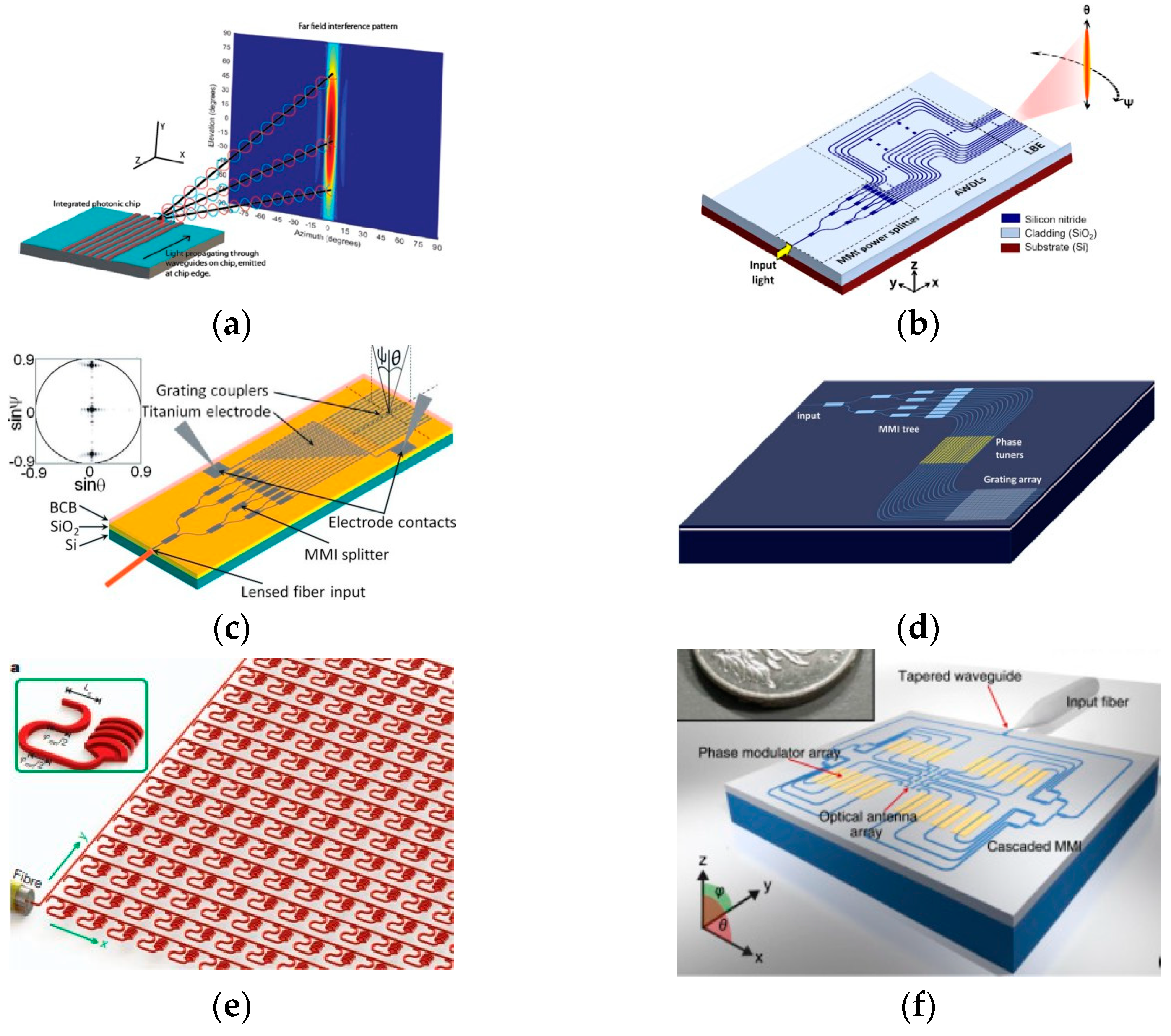
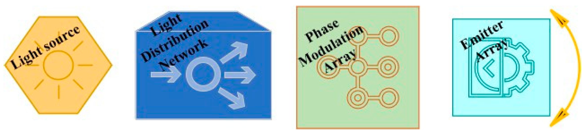
2. Basic Configuration of PIC-OPA
3. Component-Level Designing Concerns
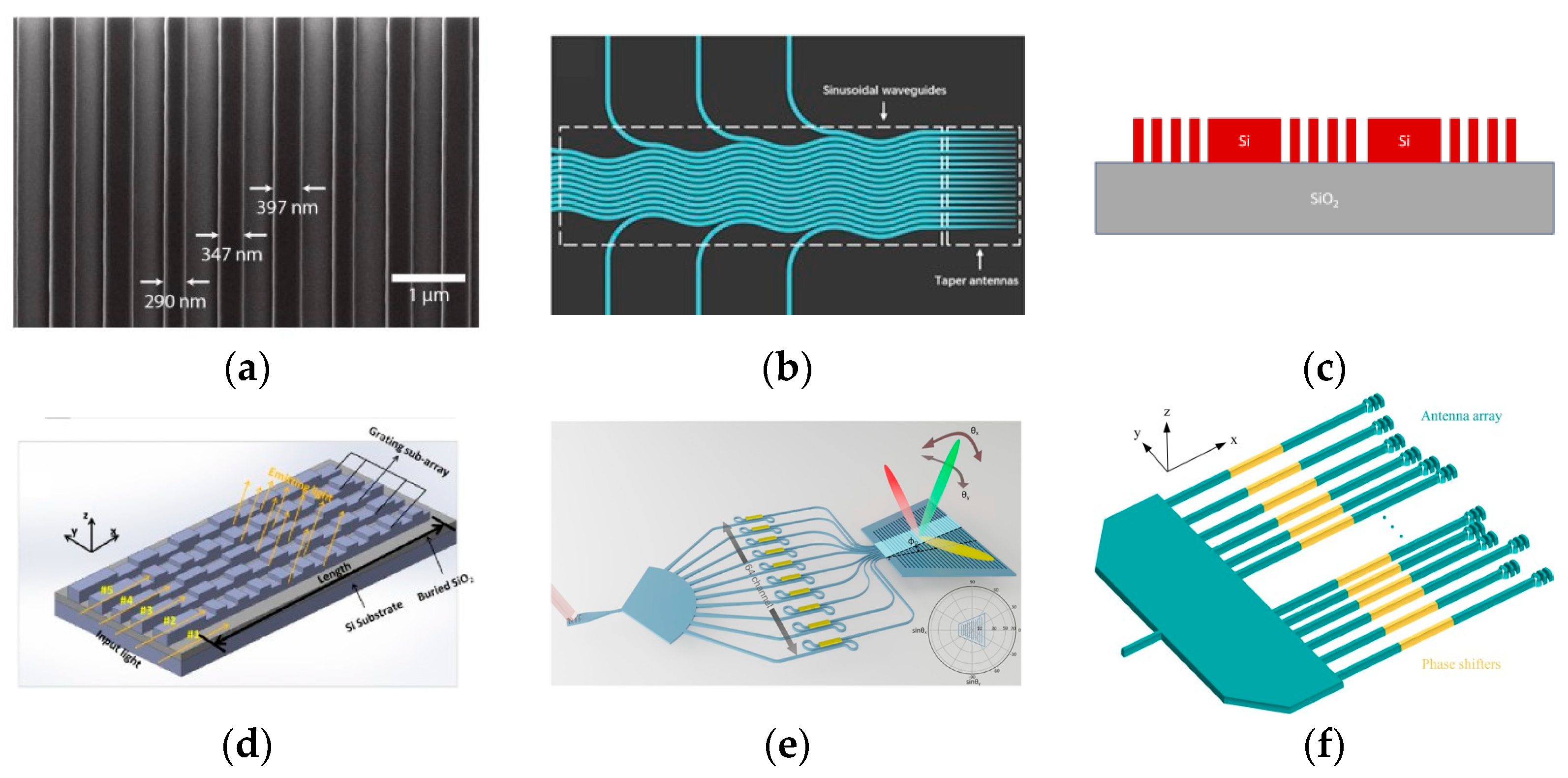
3.1. Emitter Array
3.1.1. Emitter Type
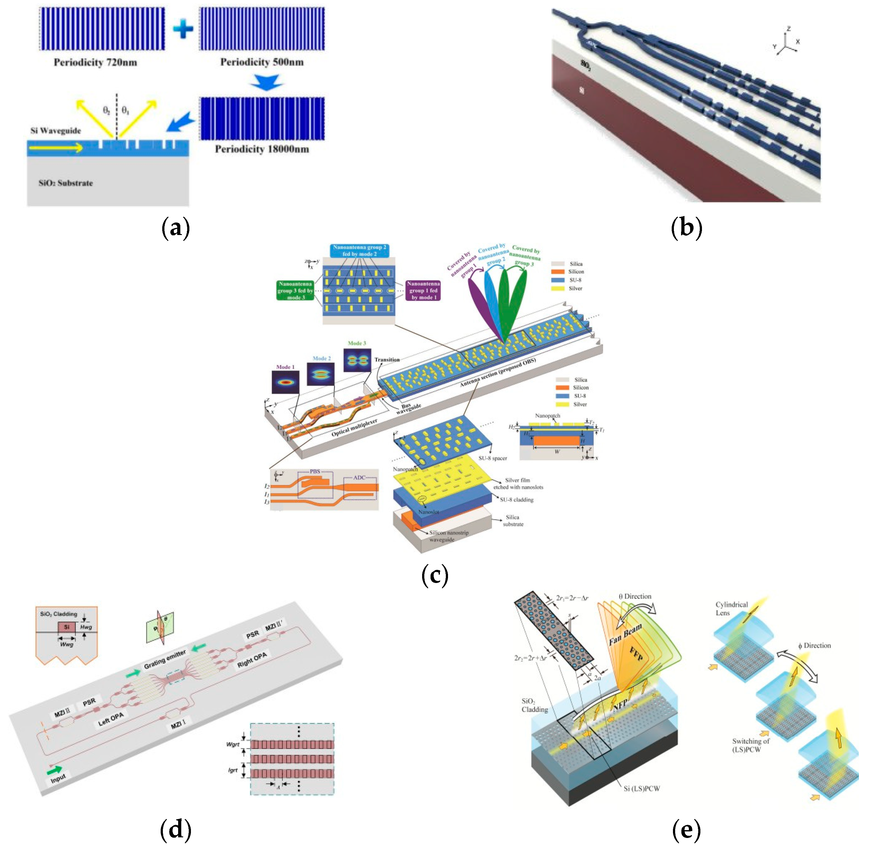
- End-Fire Array
- Waveguide Grating Array
- Nano-antenna Array
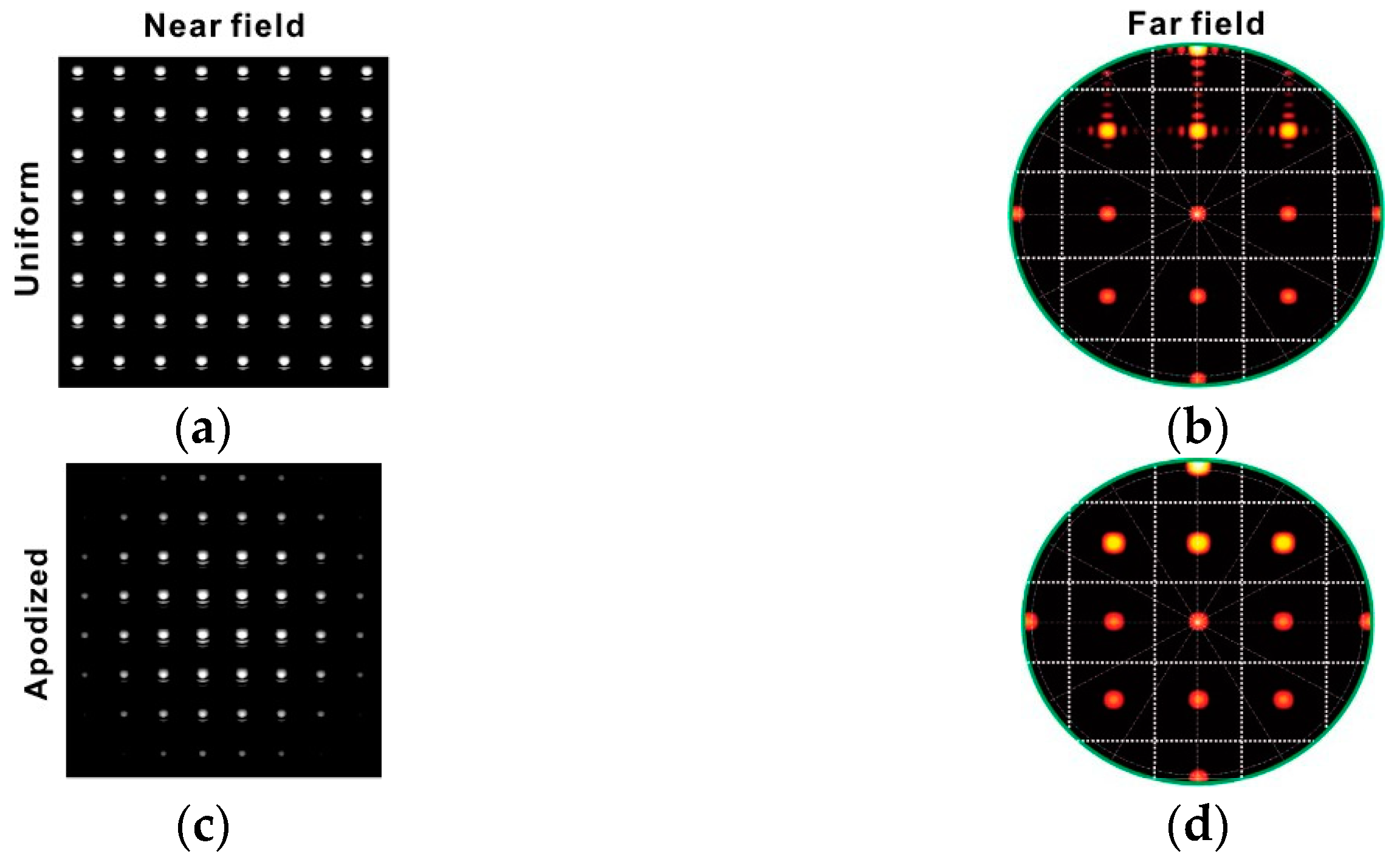
3.1.2. Emitter Envelope Function
3.1.3. Emitter Arrangement
- Aperiodic Arrangement
- Challenge the Half-Wavelength Pitch Criteria (Table 1)

| Reference | Number of Waveguides | Pitch | Width | Crosstalk | SLL |
|---|---|---|---|---|---|
| [36] | 24 | 1.3 µm | 280 nm | −12 dB | - |
| [37] | 64 | 775 nm | 300/400/350 nm | −17 dB | −11.4 dB |
| [38] | 16 | 695 nm | 500 nm | −26 dB | - |
| [39] | 8 | 695 nm | 50 nm | −25 dB | - |
| [40] | 16 | 695 nm | 500 nm | −19 dB | −10.9 dB |
| [41] | 64 | 1.2 µm/775 nm | 560/400/580/380 nm | −13 dB | −19 dB |
| [42] | 16 | 4 µm | 290 nm | No crosstalk | −5 to −10 dB |
| [31] | 9 × 9 | 20 µm | - | −6 dB | |
| [33] | 1 × 64 | 87.5 µm | 1.5 µm | No crosstalk | −20 dB |
| [35] | 820 | 9 µm | - | - | −10 dB |
| [43] | 1024 | 4 µm | 1.5 µm | - | −10 dB |
| [44] | 8 × 8 | - | 0.4 µm | - | −25 dB |
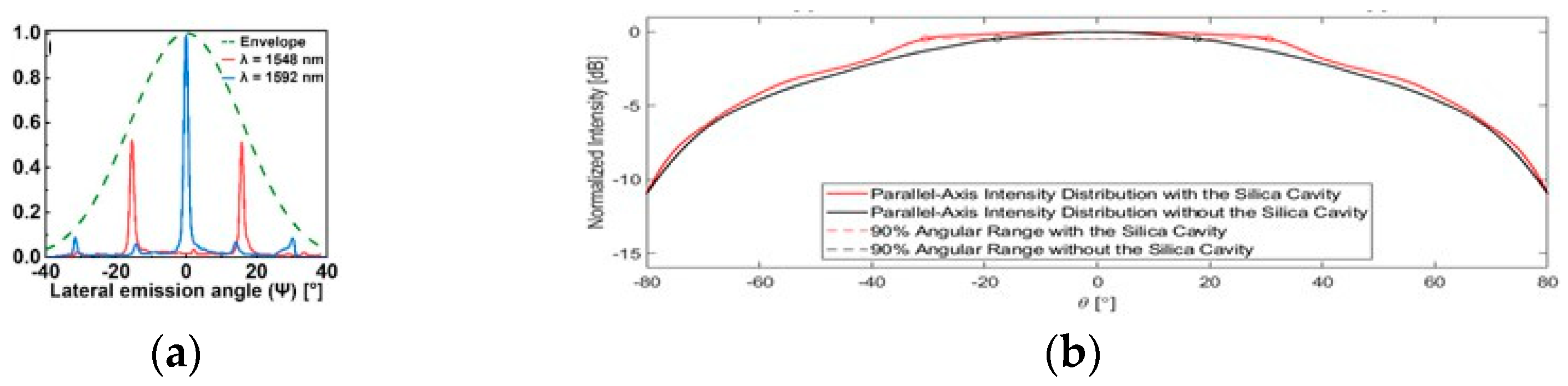
3.1.4. Emitting Aperture and Intensity Profile
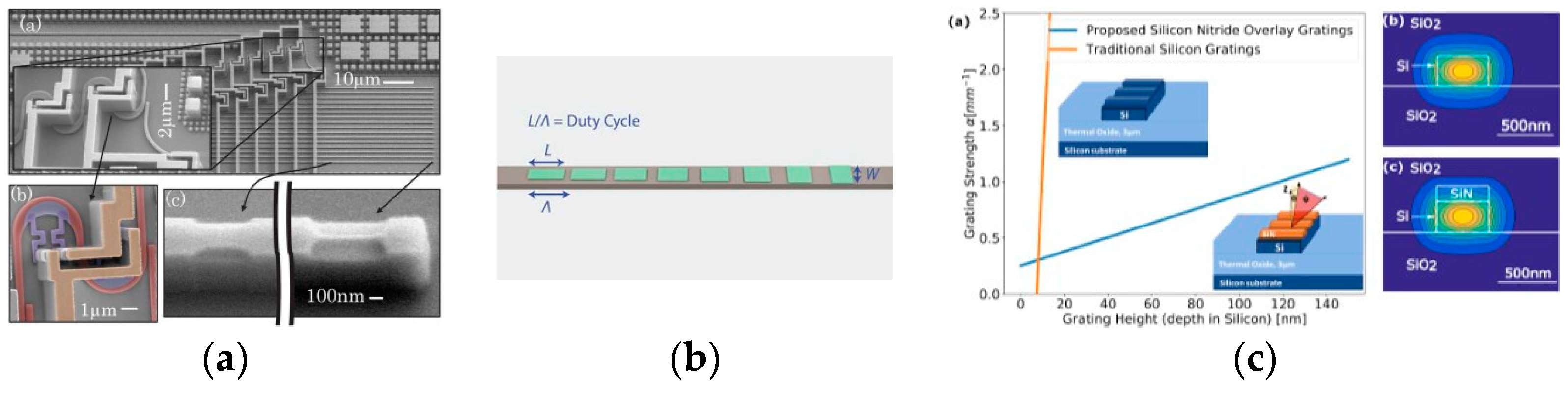
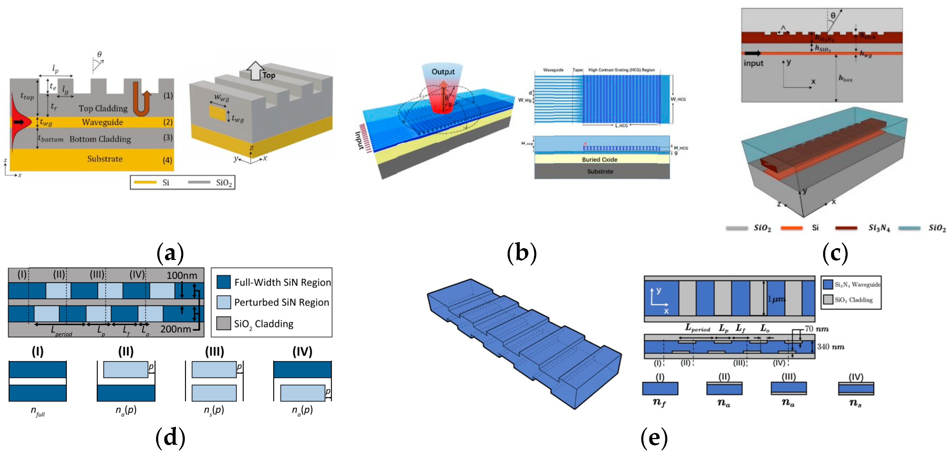
3.1.5. Waveguide Grating Coupler Design
Steering Range
Effective Aperture
Emitting Directionality
3.2. Phase Shifters
- Thermo-Optic Phase Shifter.
- Electric–Optic Phase Shifter.
- Reducing the Required Number of Phase Shifters (Table 2)
3.3. On-Chip Light Source
4. Phase Calibration and On-Chip Emitting Monitoring
5. System-Level OPA Designs
5.1. Passive OPAs
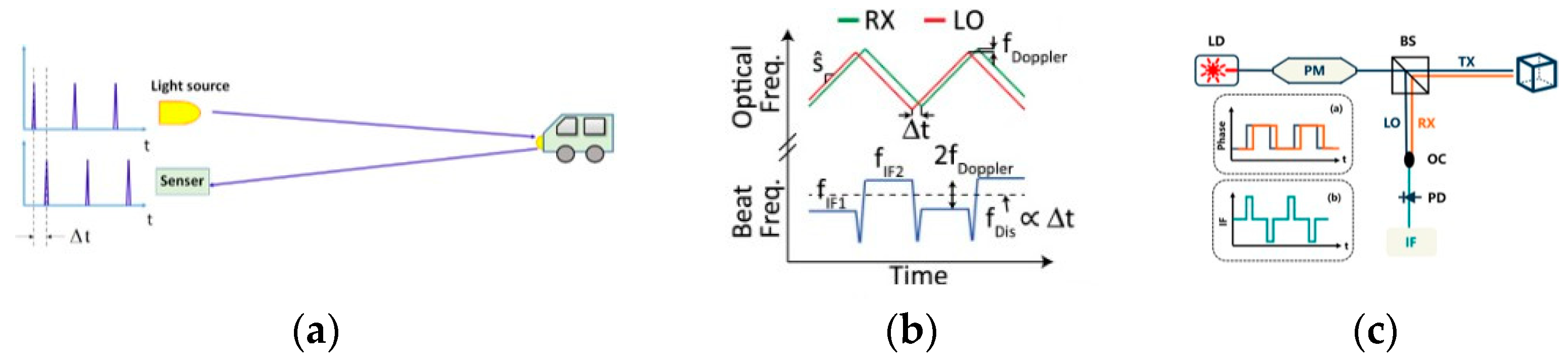
5.2. Distance Detection for LiDAR Application
5.3. Other Material Platforms
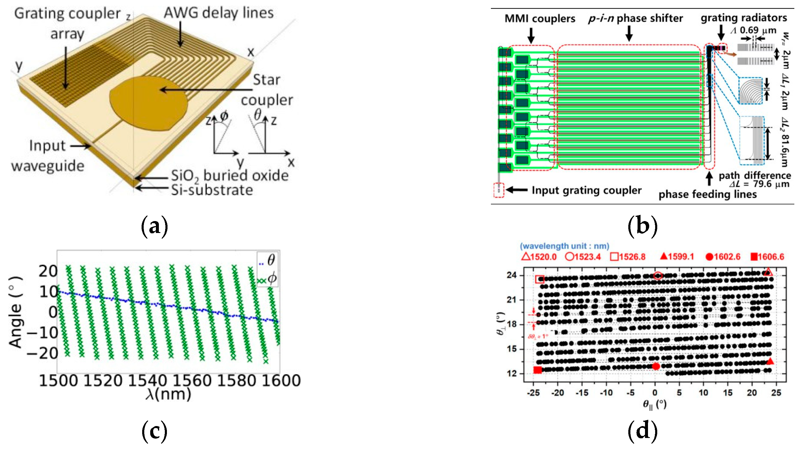
- Silicon Nitride (SiN) and Germanium–Silicon (Ge-Si)
- III–IV materials
5.4. Other Applications
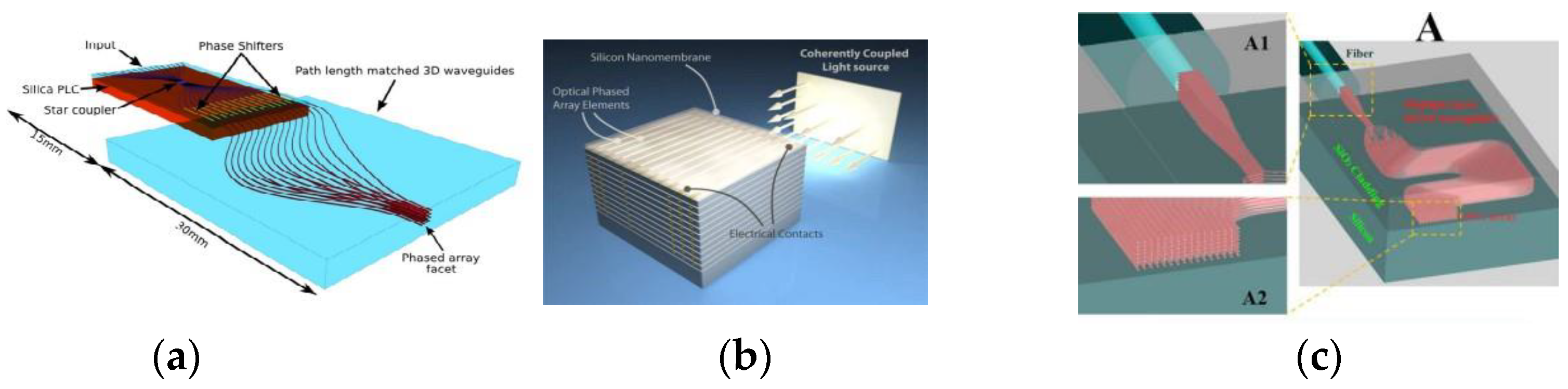
6. Three-Dimensional OPAs
7. Summary
Author Contributions
Funding
Conflicts of Interest
References
- Heck, M.J. Highly integrated optical phased arrays: Photonic integrated circuits for optical beam shaping and beam steering. Nanophotonics 2017, 6, 93–107. [Google Scholar] [CrossRef]
- Sun, X.; Zhang, L.; Zhang, Q.; Zhang, W. Si Photonics for Practical LiDAR Solutions. Appl. Sci. 2019, 9, 4225. [Google Scholar] [CrossRef]
- Hashemi, H. A Review of Semiconductor-Based Monolithic Optical Phased Array Architectures. IEEE Open J. Solid-State Circuits Soc. 2021, 1, 222–234. [Google Scholar] [CrossRef]
- Guo, Y.; Guo, Y.; Li, C.; Zhang, H.; Zhou, X.; Zhang, L. Integrated Optical Phased Arrays for Beam Forming and Steering. Appl. Sci. 2021, 11, 4017. [Google Scholar] [CrossRef]
- Kim, I.; Martins, R.J.; Jang, J.; Badloe, T.; Khadir, S.; Jung, H.Y.; Kim, H.; Kim, J.; Genevet, P.; Rho, J. Nanophotonics for light detection and ranging technology. Nat. Nanotechnol. 2021, 16, 508–524. [Google Scholar] [CrossRef]
- Hsu, C.Y.; Yiu, G.Z.; Chang, Y.C. Free-Space Applications of Silicon Photonics: A Review. Micromachines 2022, 13, 990. [Google Scholar] [CrossRef]
- Wight, D.R.; Heaton, J.M.; Hughes, B.T.; Birbeck, J.C.H.; Hilton, K.P.; Taylor, D.J. Novel phased array optical scanning device implemented using GaAs/AlGaAs technology. Appl. Phys. Lett. 1991, 59, 899–901. [Google Scholar] [CrossRef]
- Qin, C.; Shang, K.; Feng, S.; Liu, G.; Liu, G.; Pathak, S.; Yoo, S.J.B. 1 × 256 Multi-layer, low-loss, Si3N4 waveguide optical phased arrays with 0.050° Instantaneous-Field-of-View. In Proceedings of the Conference on Lasers and Electro-Optics, Munich, Germany, 25–29 June 2017; Optica Publishing Group: Washington, DC, USA, 2017; p. STh1M.2. [Google Scholar] [CrossRef]
- Kossey, M.R.; Rizk, C.; Foster, A.C. End-fire silicon optical phased array with half-wavelength spacing. APL Photonics 2017, 3, 011301. [Google Scholar] [CrossRef]
- Bhandari, B.; Wang, C.; Gwon, J.Y.; Heo, J.M.; Ko, S.Y.; Oh, M.C.; Lee, S.S. Dispersive silicon–nitride optical phased array incorporating arrayed waveguide delay lines for passive line beam scanning. Sci. Rep. 2022, 12, 18759. [Google Scholar] [CrossRef]
- Acoleyen, K.V.; Bogaerts, W.; Jágerská, J.; Thomas, N.L.; Houdré, R.; Baets, R. Off-chip beam steering with a one-dimensional optical phased array on silicon-on-insulator. Opt. Lett. 2009, 34, 1477–1479. [Google Scholar] [CrossRef]
- Doylend, J.K.; Heck, M.J.R.; Bovington, J.T.; Peters, J.D.; Coldren, L.A.; Bowers, J.E. Two-dimensional free-space beam steering with an optical phased array on silicon-on-insulator. Opt. Express 2011, 19, 21595–21604. [Google Scholar] [CrossRef]
- Sun, J.; Timurdogan, E.; Yaacobi, A.; Hosseini, E.S.; Watts, M.R. Large-scale nanophotonic phased array. Nature 2013, 493, 195–199. [Google Scholar] [CrossRef]
- Zhang, H.; Zhang, Z.; Lv, J.; Peng, C.; Hu, W. Fast beam steering enabled by a chip-scale optical phased array with 8 × 8 elements. Opt. Commun. 2020, 461, 125267. [Google Scholar] [CrossRef]
- Vasey, F.; Reinhart, F.K.; Houdré, R.; Stauffer, J.M. Spatial optical beam steering with an AlGaAs integrated phased array. Appl. Opt. 1993, 32, 3220–3232. [Google Scholar] [CrossRef]
- Acoleyen, K.V.; Komorowska, K.; Bogaerts, W.; Baets, R. One-Dimensional Off-Chip Beam Steering and Shaping Using Optical Phased Arrays on Silicon-on-Insulator. J. Light. Technol. 2011, 29, 3500–3505. [Google Scholar] [CrossRef]
- Kwong, D.; Hosseini, A.; Covey, J.; Zhang, Y.; Xu, X.; Subbaraman, H.; Chen, R.T. On-chip silicon optical phased array for two-dimensional beam steering. Opt. Lett. 2014, 39, 941–944. [Google Scholar] [CrossRef] [PubMed]
- Sun, J.; Timurdogan, E.; Yaacobi, A.; Su, Z.; Hosseini, E.S.; Cole, D.B.; Watts, M.R. Large-Scale Silicon Photonic Circuits for Optical Phased Arrays. IEEE J. Sel. Top. Quantum Electron. 2014, 20, 264–278. [Google Scholar] [CrossRef]
- Xu, W.; Zhou, L.; Lu, L.; Chen, J. Aliasing-free optical phased array beam-steering with a plateau envelope. Opt. Express 2019, 27, 3354–3368. [Google Scholar] [CrossRef]
- Shin, M.C.; Mohanty, A.; Watson, K.; Bhatt, G.R.; Phare, C.T.; Miller, S.A.; Zadka, M.; Lee, B.S.; Ji, X.; Datta, I.; et al. Chip-scale blue light phased array. Opt. Lett. 2020, 45, 1934–1937. [Google Scholar] [CrossRef]
- Hutchison, D.N.; Sun, J.; Doylend, J.K.; Kumar, R.; Heck, J.; Kim, W.; Phare, C.T.; Feshali, A.; Rong, H. High-resolution aliasing-free optical beam steering. Optica 2016, 3, 887–890. [Google Scholar] [CrossRef]
- Fatemi, R.; Khachaturian, A.; Hajimiri, A. A nonuniform sparse 2-D large-FOV optical phased array with a low-power PWM drive. IEEE J. Solid-State Circuits 2019, 54, 1200–1215. [Google Scholar] [CrossRef]
- Liu, Q.; Benedikovic, D.; Smy, T.; Atieh, A.; Cheben, P.; Ye, W.N. Circular Optical Phased Arrays with Radial Nano-Antennas. Nanomaterials 2022, 12, 1938. [Google Scholar] [CrossRef]
- Komljenovic, T.; Helkey, R.; Coldren, L.; Bowers, J.E. Sparse aperiodic arrays for optical beam forming and LIDAR. Opt. Express 2017, 25, 2511–2528. [Google Scholar] [CrossRef]
- Zhuang, D.; Zhagn, L.; Han, X.; Li, Y.; Li, Y.; Liu, X.; Gao, F.; Song, J. Omnidirectional beam steering using aperiodic optical phased array with high error margin. Opt. Express 2018, 26, 19154–19170. [Google Scholar] [CrossRef] [PubMed]
- Yang, B.; Chen, H.; Yang, S.; Chen, M. An improved aperiodic OPA design based on large antenna spacing. Opt. Commun. 2020, 475, 125852. [Google Scholar] [CrossRef]
- Du, K.; Wang, R.; Guo, J.; Jiang, R.; Kan, D.; Zhang, Y. Design of a sparse array for a one-dimensional non-uniform optical phased array. J. Opt. Soc. Am. B 2022, 39, 1141–1146. [Google Scholar] [CrossRef]
- Kwong, D.; Hosseini, A.; Zhang, Y.; Chen, R.T. 1 × 12 Unequally spaced waveguide array for actively tuned optical phased array on a silicon nanomembrane. Appl. Phys. Lett. 2011, 99, 051104. [Google Scholar] [CrossRef]
- Shin, D.; Lee, J.; Hwang, I.; Otsuka, T.; Lee, C.; Shim, D.; Lee, E.; Ha, K.; Ryu, H.Y.; Choo, H.; et al. Aperiodic optical phased array based on number theory. Optica, 2023; preprint. [Google Scholar] [CrossRef]
- Kazemian, A.; Wang, P.; Zhuang, Y.; Yi, Y. Optimization of the silicon-based aperiodic optical phased array antenna. Opt. Lett. 2021, 46, 801–804. [Google Scholar] [CrossRef]
- Xue, Y.; Zhang, Q.; Ren, Y.; Lei, Y.; Sun, X.; Zhang, L. Two-dimensional single-lobe Si photonic optical phased array with minimal antennas using a non-uniform large spacing array design. Appl. Opt. 2022, 61, 7158–7162. [Google Scholar] [CrossRef]
- Zhang, F.; Zhang, D.; Pan, S. Fast and wide-range optical beam steering with ultralow side lobes by applying an optimized multi-circular optical phased array. Appl. Opt. 2018, 57, 4977–4984. [Google Scholar] [CrossRef] [PubMed]
- Wang, P.; Luo, G.; Li, Y.; Wang, M.; Meng, F.; Yang, W.; Yu, H.; Zhou, X.; Zhang, Y.; Pan, J. Two-dimensional large-angle scanning optical phased array with single wavelength beam. In Proceedings of the CLEO: Applications and Technology, San Jose, CA, USA, 13–18 May 2018; Optica Publishing Group: Washington, DC, USA, 2019; p. JTh2A–72. [Google Scholar]
- Liu, X.; Xiong, B.; Sun, C.; Hao, Z.; Wang, L.; Wang, J.; Han, Y.; Li, H.; Luo, Y. Circular optical phased array for 360 constant amplitude scanning. In Proceedings of the 10th International Conference on Information Optics and Photonics, San Diego, CA, USA, 27 September 2018; SPIE: Bellingham, WA, USA, 2018; Volume 10964, pp. 1044–1048. [Google Scholar]
- Benedikovič, D.; Liu, Q.; Sánchez-Postigo, A.; Atieh, A.; Smy, T.; Cheben, P.; Ye, W.N. Circular optical phased array with large steering range and high resolution. Sensors 2022, 22, 6135. [Google Scholar] [CrossRef] [PubMed]
- Zhang, Y.; Ling, Y.C.; Zhang, K.; Gentry, C.; Sadighi, D.; Whaley, G.; Colosimo, J.; Suni, P.; Yoo, S.B. Sub-wavelength-pitch silicon-photonic optical phased array for large field-of-regard coherent optical beam steering. Opt. Express 2019, 27, 1929–1940. [Google Scholar] [CrossRef] [PubMed]
- Phare, C.T.; Shin, M.C.; Sharma, J.; Ahasan, S.; Krishnaswamy, H.; Lipson, M. Silicon optical phased array with grating lobe-free beam formation over 180 degree field of view. In Proceedings of the CLEO: Science and Innovations, San Jose, CA, USA, 13–18 May 2018; Optica Publishing Group: Washington, DC, USA, 2018; p. SM3I-2. [Google Scholar]
- Yi, X.; Zeng, H.; Gao, S.; Qiu, C. Design of an ultra-compact low-crosstalk sinusoidal silicon waveguide array for optical phased array. Opt. Express 2020, 28, 37505–37513. [Google Scholar] [CrossRef]
- Yi, X.; Zhang, Y.; Zeng, H.; Gao, S.; Guo, S.; Qiu, C. Demonstration of an Ultra-compact 8-channel sinusoidal silicon waveguide array for optical phased array. Opt. Lett. 2022, 47, 226–229. [Google Scholar] [CrossRef] [PubMed]
- Liang, D.; Li, W.; Wang, X.; Zhao, X.; Guo, Z.; Han, X.; Chen, J.; Dai, D.; Shi, Y. Grating lobe-free silicon optical phased array with periodically bending modulation of dense antennas. Opt. Express 2023, 31, 11423–11430. [Google Scholar] [CrossRef]
- Liu, Y.; Hu, H. Silicon optical phased array with a 180-degree field of view for 2D optical beam steering. Optica 2022, 9, 903–907. [Google Scholar] [CrossRef]
- Kwong, D.; Hosseini, A.; Covey, J.; Xu, X.; Zhang, Y.; Chakravarty, S.; Chen, R.T. Corrugated waveguide-based optical phased array with crosstalk suppression. IEEE Photonics Technol. Lett. 2014, 26, 991–994. [Google Scholar] [CrossRef]
- Poulton, C.V.; Byrd, M.J.; Raval, M.; Su, Z.; Li, N.; Timurdogan, E.; Coolbaugh, D.; Vermeulen, D.; Watts, M.R. Large-scale silicon nitride nanophotonic phased arrays at infrared and visible wavelengths. Opt. Lett. 2017, 42, 21–24. [Google Scholar] [CrossRef]
- Sun, J.; Shah Hosseini, E.; Yaacobi, A.; Cole, D.B.; Leake, G.; Coolbaugh, D.; Watts, M.R. Two-dimensional apodized silicon photonic phased arrays. Opt. Lett. 2014, 39, 367–370. [Google Scholar] [CrossRef]
- Kong, Z. Design and Characterization of Optical Phased Array with Half-Wavelength Spacing. Ph.D. Thesis, Purdue University Graduate School, West Lafayette, IN, USA, 2021. [Google Scholar]
- Wu, Z.; Jiang, W.; Xia, J.; Huang, Q. Optical phased array antenna with wide steering range using grating array superlattices. In Proceedings of the 6th International Conference on Optical and Photonic Engineering (icOPEN 2018), Shanghai, China, 8–11 May 2018; SPIE: Bellingham, WA, USA, 2018; Volume 10827, pp. 645–650. [Google Scholar]
- Lei, Y.; Zhang, L.; Xue, Y.; Ren, Y.; Zhang, Q.; Zhang, W.; Sun, X. Effective half-wavelength pitch optical phased array design for aliasing-free 2D beam steering. Appl. Opt. 2022, 61, 9423–9428. [Google Scholar] [CrossRef]
- Dostart, N.; Zhang, B.; Khilo, A.; Brand, M.; Al Qubaisi, K.; Onural, D.; Feldkhun, D.; Wagner, K.H.; Popovic, M.A. Serpentine optical phased arrays for scalable integrated photonic lidar beam steering. Optica 2020, 7, 726–733. [Google Scholar] [CrossRef]
- Im, C.S.; Bhandari, B.; Lee, K.P.; Kim, S.M.; Oh, M.C.; Lee, S.S. Silicon nitride optical phased array based on a grating antenna enabling wavelength-tuned beam steering. Opt. Express 2020, 28, 3270–3279. [Google Scholar] [CrossRef]
- Wu, D.; Guo, W.; Yi, Y. Compound period grating coupler for double beam generation and steering. Appl. Opt. 2019, 58, 361–367. [Google Scholar] [CrossRef]
- Liu, Y.; Hao, Z.; Wang, L.; Xiong, B.; Sun, C.; Wang, J.; Li, H.; Han, Y.; Luo, Y. A single-chip multi-beam steering optical phased array: Design rules and simulations. Opt. Express 2021, 29, 7049–7059. [Google Scholar] [CrossRef]
- Zeng, Y.; Qu, S.; Wu, J. Polarization-division and spatial-division shared-aperture nanopatch antenna arrays for wide-angle optical beam scanning. Opt. Express 2020, 28, 12805–12826. [Google Scholar] [CrossRef]
- Zhao, S.; Chen, J.; Shi, Y. Dual polarization and bi-directional silicon-photonic optical phased array with large scanning range. IEEE Photonics J. 2022, 14, 6620905. [Google Scholar] [CrossRef]
- Abe, H.; Takeuchi, M.; Takeuchi, G.; Ito, H.; Yokokawa, T.; Kondo, K.; Furukado, Y.; Baba, T. Two-dimensional beam-steering device using a doubly periodic Si photonic-crystal waveguide. Opt. Express 2018, 26, 9389–9397. [Google Scholar] [CrossRef] [PubMed]
- Kondo, K.; Tatebe, T.; Hachuda, S.; Abe, H.; Koyama, F.; Baba, T. Fan-beam steering device using a photonic crystal slow-light waveguide with surface diffraction grating. Opt. Lett. 2017, 42, 4990–4993. [Google Scholar] [CrossRef] [PubMed]
- Takeuchi, G.; Terada, Y.; Takeuchi, M.; Abe, H.; Ito, H.; Baba, T. Thermally controlled Si photonic crystal slow light waveguide beam steering device. Opt. Express 2018, 26, 11529–11537. [Google Scholar] [CrossRef] [PubMed]
- Gondo, J.; Ito, H.; Tamanuki, T.; Baba, T. Space-time-domain observation of high-speed optical beam scanning in a thermo-optic Si photonic crystal slow-light beam scanner. Opt. Lett. 2021, 46, 3600–3603. [Google Scholar] [CrossRef] [PubMed]
- Yaacobi, A.; Sun, J.; Moresco, M.; Leake, G.; Coolbaugh, D.; Watts, M.R. Integrated phased array for wide-angle beam steering. Opt. Lett. 2014, 39, 4575–4578. [Google Scholar] [CrossRef]
- Shang, K.; Qin, C.; Zhang, Y.; Liu, G.; Xiao, X.; Feng, S.; Yoo, S. Uniform emission, constant wavevector silicon grating surface emitter for beam steering with ultra-sharp instantaneous field-of-view. Opt. Express 2017, 25, 19655–19661. [Google Scholar] [CrossRef] [PubMed]
- Zadka, M.; Chang, Y.C.; Mohanty, A.; Phare, C.T.; Roberts, S.P.; Lipson, M. On-chip platform for a phased array with minimal beam divergence and wide field-of-view. Opt. Express 2018, 26, 2528–2534. [Google Scholar] [CrossRef]
- Zhang, Z.; Yu, H.; Chen, B.; Xia, P.; Zhou, Z.; Huang, Q.; Dai, T.; Wang, Y.; Yang, J. A Tri-Layer SiN-on-Si Optical Phased Array With High Angular Resolution. IEEE Photonics Technol. Lett. 2022, 34, 1108–1111. [Google Scholar] [CrossRef]
- Han, K.; Yurlov, V.; Yu, N.E. Highly directional waveguide grating antenna for optical phased array. Curr. Appl. Phys. 2018, 18, 824–828. [Google Scholar] [CrossRef]
- Wang, P.; Luo, G.; Yu, H.; Li, Y.; Wang, M.; Zhou, X.; Chen, W.; Zhang, Y.; Pan, J. Improving the performance of optical antenna for optical phased arrays through high-contrast grating structure on SOI substrate. Opt. Express 2019, 27, 2703–2712. [Google Scholar] [CrossRef]
- Wang, Q.; Wang, S.; Zeng, Y.; Wang, W.; Cai, Y.; Tu, Z.; Yue, W.; Wang, X.; Fang, Q.; Yu, M. Dual-layer waveguide grating antenna with high directionality for optical phased arrays. Appl. Opt. 2019, 58, 5807–5811. [Google Scholar] [CrossRef]
- Raval, M.; Poulton, C.V.; Watts, M.R. Unidirectional waveguide grating antennas with uniform emission for optical phased arrays. Opt. Lett. 2017, 42, 2563–2566. [Google Scholar] [CrossRef]
- Chen, B.; Li, Y.; Zhang, L.; Li, Y.; Liu, X.; Tao, M.; Hou, Y.; Tang, H.; Zhi, Z.; Gao, F.; et al. Unidirectional large-scale waveguide grating with uniform radiation for optical phased array. Opt. Express 2021, 29, 20995–21010. [Google Scholar] [CrossRef]
- Kim, S.H.; You, J.B.; Ha, Y.G.; Kang, G.; Lee, D.S.; Yoon, H.; Yoo, D.E.; Lee, D.W.; Yu, K.; Youn, C.H.; et al. Thermo-optic control of the longitudinal radiation angle in a silicon-based optical phased array. Opt. Lett. 2019, 44, 411–414. [Google Scholar] [CrossRef]
- Yang, B.; Chen, H.; Yang, S.; Chen, M. A design method of optical phased array with insufficient phase tuning range. IEEE Photonics J. 2020, 12, 1–9. [Google Scholar] [CrossRef]
- Wang, Y.; Liang, L.; Chen, Y.; Jia, P.; Qin, L.; Liu, Y.; Ning, Y.; Wang, L. Improved performance of optical phased arrays assisted by transparent graphene nanoheaters and air trenches. RSC Adv. 2018, 8, 8442–8449. [Google Scholar] [CrossRef] [PubMed]
- Kim, S.M.; Park, T.H.; Im, C.S.; Lee, S.S.; Kim, T.; Oh, M.C. Temporal response of polymer waveguide beam scanner with thermo-optic phase-modulator array. Opt. Express 2020, 28, 3768–3778. [Google Scholar] [CrossRef] [PubMed]
- Larocque, H.; Ranzani, L.; Leatham, J.; Tate, J.; Niechayev, A.; Yengst, T.; Komljenovic, T.; Fodran, C.; Smith, D.; Soltani, M. Beam steering with ultracompact and low-power silicon resonator phase shifters. Opt. Express 2019, 27, 34639–34654. [Google Scholar] [CrossRef] [PubMed]
- Miller, S.A.; Chang, Y.C.; Phare, C.T.; Shin, M.C.; Zadka, M.; Roberts, S.P.; Stern, B.; Ji, X.; Mohanty, A.; Gordillo, O.A.J.; et al. Large-scale optical phased array using a low-power multi-pass silicon photonic platform. Optica 2020, 7, 3–6. [Google Scholar] [CrossRef]
- Kang, G.; Kim, S.H.; You, J.B.; Lee, D.S.; Yoon, H.; Ha, Y.G.; Kim, J.H.; Yoo, D.E.; Lee, D.W.; Youn, C.H.; et al. Silicon-Based Optical Phased Array Using Electro-Optic p-i-n Phase Shifters. IEEE Photonics Technol. Lett. 2019, 31, 1685–1688. [Google Scholar] [CrossRef]
- Xie, W.; Bowers, J. High-performance III-V/Si Phase Shifter Arrays for Beam Steering. In Proceedings of the 2019 IEEE Photonics Society Summer Topical Meeting Series (SUM), Lauderdale, FL, USA, 8–10 July 2019; pp. 1–2. [Google Scholar]
- Hirano, Y.; Miyamoto, Y.; Miura, M.; Motoyama, Y.; Machida, K.; Yamada, T.; Otomo, A.; Kikuchi, H. High-speed optical-beam scanning by an optical phased array using electro-optic polymer waveguides. IEEE Photonics J. 2020, 12, 6600807. [Google Scholar] [CrossRef]
- Poulton, C.V.; Byrd, M.J.; Russo, P.; Moss, B.; Shatrovoy, O.; Khandaker, M.; Watts, M.R. Coherent LiDAR with an 8,192-element optical phased array and driving laser. IEEE J. Sel. Top. Quantum Electron. 2022, 28, 6100508. [Google Scholar] [CrossRef]
- Rabinovich, W.S.; Goetz, P.G.; Pruessner, M.; Mahon, R.; Ferraro, M.S.; Park, D.; Fleet, E.; DePrenger, M.J. Free space optical communication link using a silicon photonic optical phased array. In Proceedings of the Free-Space Laser Communication and Atmospheric Propagation XXVII, San Francisco, CA, USA, 16 March 2015; SPIE: Bellingham, WA, USA, 2015; Volume 9354, pp. 96–101. [Google Scholar]
- Poulton, C.V.; Yaacobi, A.; Cole, D.B.; Byrd, M.J.; Raval, M.; Vermeulen, D.; Watts, M.R. Coherent solid-state LIDAR with silicon photonic optical phased arrays. Opt. Lett. 2017, 42, 4091–4094. [Google Scholar] [CrossRef]
- Li, W.; Chen, J.; Liang, D.; Dai, D.; Shi, Y. Silicon optical phased array with calibration-free phase shifters. Opt. Express 2022, 30, 44029–44038. [Google Scholar] [CrossRef]
- Ashtiani, F.; Aflatouni, F. N×N optical phased array with 2N phase shifters. Opt. Express 2019, 27, 27183–27190. [Google Scholar] [CrossRef]
- Wu, D.; Yu, B.; Yi, Y. Phase-combining unit for aliasing suppression in an optical phased array. Opt. Lett. 2022, 47, 1996–1999. [Google Scholar] [CrossRef]
- Han, Y.; Park, H.; Bowers, J.; Lau, K. Recent advances in light sources on silicon. Adv. Opt. Pho. 2022, 14, 404–453. [Google Scholar] [CrossRef]
- Doylend, J.; Heck, M.; Bovington, J.; Peters, J.; Davenport, M.; Coldren, L.; Bowers, J. Hybrid III/V silicon photonic source with integrated 1D free-space beam steering. Opt. Lett. 2012, 37, 4257–4259. [Google Scholar] [CrossRef] [PubMed]
- Guo, W.; Binetti, P.R.; Althouse, C.; Mašanovic´, M.L.; Ambrosius, H.P.; Johansson, L.A.; Coldren, L.A. Two-dimensional optical beam steering with InP-based photonic integrated circuits. IEEE J. Sel. Top. Quantum Electron. 2013, 19, 6100212. [Google Scholar] [CrossRef]
- Hulme, J.; Doylend, J.; Heck, M.; Peters, J.; Davenport, M.; Bovington, J.; Coldren, L.; Bowers, J. Fully integrated hybrid silicon free-space beam steering source with 32-channel phased array. In Proceedings of the Smart Photonic and Optoelectronic Integrated Circuits XVI, San Francisco, CA, USA, 2–5 February 2019; SPIE: Bellingham, WA, USA, 2014; Volume 8989, pp. 18–32. [Google Scholar]
- Hulme, J.; Doylend, J.; Heck, M.; Peters, J.; Davenport, M.; Bovington, J.; Coldren, L.; Bowers, J. Fully integrated hybrid silicon two dimensional beam scanner. Opt. Express 2015, 23, 5861–5874. [Google Scholar] [CrossRef]
- Notaros, J.; Li, N.; Poulton, C.V.; Su, Z.; Byrd, M.J.; Magden, E.S.; Timurdogan, E.; Baiocco, C.; Fahrenkopf, N.M.; Watts, M.R. CMOS-compatible optical phased array powered by a monolithically-integrated erbium laser. J. Light. Technol. 2019, 37, 5982–5987. [Google Scholar] [CrossRef]
- Yue, J.; Cui, A.; Wang, F.; Han, L.; Dai, J.; Sun, X.; Lin, H.; Wang, C.; Chen, C.; Zhang, D. Design of Monolithic 2D Optical Phased Arrays Heterogeneously Integrated with On-Chip Laser Arrays Based on SOI Photonic Platform. Micromachines 2022, 13, 2117. [Google Scholar] [CrossRef] [PubMed]
- Misugi, Y.; Okayama, H.; Kita, T. Compact and Low Power-Consumption Solid-State Two-Dimensional Beam Scanner Integrating a Passive Optical Phased Array and Hybrid Wavelength-Tunable Laser Diode. J. Light. Technol. 2023, 41, 3505–3512. [Google Scholar] [CrossRef]
- Zhou, J.; Sun, J.; Yaacobi, A.; Poulton, C.V.; Watts, M.R. Design of 3D hologram emitting optical phased arrays. In Proceedings of the Integrated Photonics Research, Silicon and Nanophotonics, Boston, MA, USA, 27 June–1 July 2015; Optica Publishing Group: Washington, DC, USA, 2015; p. IT4A-7. [Google Scholar]
- Guerber, S.; Fowler, D.; Faugier-Tovar, J.; Carim, K.A.; Delplanque, B.; Szelag, B. Wafer-level calibration of large-scale integrated optical phased arrays. Opt. Express 2022, 30, 35246–35255. [Google Scholar] [CrossRef] [PubMed]
- Komljenovic, T.; Pintus, P. On-chip calibration and control of optical phased arrays. Opt. Express 2018, 26, 3199–3210. [Google Scholar] [CrossRef] [PubMed]
- Zhang, W.; Li, L.; Chen, W. A chaotic stochastic parallel gradient descent algorithm for fast phase correction of optical phased array. In Proceedings of the 11th International Conference on Information Optics and Photonics (CIOP 2019), Xi’an, China, 6–9 August 2019; SPIE: Bellingham, WA, USA, 2019; Volume 11209, pp. 1277–1289. [Google Scholar]
- Jin, J.; Lee, E.S.; Chun, K.W.; Lee, S.S.; Oh, M.C. Fast-running beamforming algorithm for optical phased array beam scanners comprised of polymeric waveguide devices. Opt. Express 2022, 30, 768–779. [Google Scholar] [CrossRef] [PubMed]
- Zhang, Q.; Zhang, L.; Li, Z.; Wu, W.; Wang, G.; Sun, X.; Zhang, W. An antenna array initial condition calibration method for integrated optical phased array. arXiv 2019, arXiv:1902.06203. [Google Scholar]
- Sung, J.Y.; Lee, S.L. Fast phase error calibration through radix-p optimization processing. Opt. Express 2021, 29, 41776–41787. [Google Scholar] [CrossRef]
- Huang, Y.; Wang, K.; Yan, Q.; Wang, Y.; Wang, X.; Liu, H.; Feng, J.; Zhang, F.; Feng, Z.; Siviloglou, G.A. Universal dimension reduced phase compensation algorithm for an optical phased array. Opt. Lett. 2022, 47, 2871–2874. [Google Scholar] [CrossRef]
- Li, L.J.; Chen, W.; Zhao, X.Y.; Sun, M.J. Fast optical phased array calibration technique for random phase modulation LiDAR. IEEE Photonics J. 2018, 11, 6900410. [Google Scholar] [CrossRef]
- Zhang, H.; Zhang, Z.; Peng, C.; Hu, W. Phase calibration of on-chip optical phased arrays via interference technique. IEEE Photonics J. 2020, 12, 6600210. [Google Scholar] [CrossRef]
- Yepez, P.A.K.; Scholz, U.; Zimmermann, A. Temperature dependence of the steering angles of a silicon photonic optical phased array. IEEE Photonics J. 2020, 12, 6800813. [Google Scholar] [CrossRef]
- Shim, J.; You, J.B.; Rhee, H.W.; Yoon, H.; Kim, S.H.; Yu, K.; Park, H.H. On-chip monitoring of far-field patterns using a planar diffractor in a silicon-based optical phased array. Opt. Lett. 2020, 45, 6058–6061. [Google Scholar] [CrossRef]
- Xiao, F.; Hu, W.; Xu, A. Optical phased-array beam steering controlled by wavelength. Appl. Opt. 2005, 44, 5429–5433. [Google Scholar] [CrossRef] [PubMed]
- Kim, J.Y.; Yoon, J.; Kim, J.; Kwon, N.H.; Rhee, H.W.; Baek, M.; Lee, Y.; Park, H.H.; Yoon, H. Demonstration of beam steering using a passive silica optical phased array with wavelength tuning. Opt. Lett. 2022, 47, 4857–4860. [Google Scholar] [CrossRef] [PubMed]
- Van Acoleyen, K.; Bogaerts, W.; Baets, R. Two-dimensional dispersive off-chip beam scanner fabricated on silicon-on-insulator. IEEE Photonics Technol. Lett. 2011, 23, 1270–1272. [Google Scholar] [CrossRef]
- Yoon, H.; Rhee, H.W.; Kwon, N.H.; Kim, J.Y.; Kim, J.; Yoon, J.; Park, H.H. Demonstration of Two-Dimensional Beam Steering through Wavelength Tuning with One-Dimensional Silicon Optical Phased Array. Photonics. 2022, 9, 812. [Google Scholar] [CrossRef]
- Van Acoleyen, K.; Rogier, H.; Baets, R. Two-dimensional optical phased array antenna on silicon-on-insulator. Opt. Express 2010, 18, 13655–13660. [Google Scholar] [CrossRef]
- Martin, A.; Dodane, D.; Leviandier, L.; Dolfi, D.; Naughton, A.; O’Brien, P.; Spuessens, T.; Baets, R.; Lepage, G.; Verheyen, P.; et al. Photonic integrated circuit-based FMCW coherent LiDAR. J. Light. Technol. 2018, 36, 4640–4645. [Google Scholar] [CrossRef]
- Zhang, L.; Li, Y.; Chen, B.; Wang, Y.; Li, H.; Hou, Y.; Tao, M.; Li, Y.; Zhi, Z.; Liu, X.; et al. Two-dimensional multi-layered SiN-on-SOI optical phased array with wide-scanning and long-distance ranging. Opt. Express 2022, 30, 5008–5018. [Google Scholar] [CrossRef]
- Suyama, S.; Ito, H.; Kurahashi, R.; Abe, H.; Baba, T. Doppler velocimeter and vibrometer FMCW LiDAR with Si photonic crystal beam scanner. Opt. Express 2021, 29, 30727–30734. [Google Scholar] [CrossRef]
- Mingshi, Z.; Yubing, W.; Lanxuan, Z.; Qian, H.; Shuhua, Z.; Lei, L.; Yongyi, C.; Li, Q.; Junfeng, S.; Lijun, W. Phase-modulated continuous-wave coherent ranging method for optical phased array lidar. Opt. Express 2023, 31, 6514–6528. [Google Scholar] [CrossRef]
- Fantoni, A.; Lourenço, P.; Costa, J.; Vieira, M. Amorphous silicon photonic optical phased array for beam steering. In Proceedings of the Physics and Simulation of Optoelectronic Devices XXXI, San Francisco, CA, USA, 31 January–2 February 2023; SPIE: Bellingham, WA, USA, 2023; Volume 12415, pp. 90–98. [Google Scholar]
- Sabouri, S.; Jamshidi, K. Design considerations of silicon nitride optical phased array for visible light communications. IEEE J. Sel. Top. Quantum Electron. 2018, 24, 8300707. [Google Scholar] [CrossRef]
- Zhu, S.; Hu, T.; Li, Y.; Xu, Z.; Zhong, Q.; Dong, Y.; Singh, N. CMOS-compatible integrated silicon nitride optical phase array for electrically tunable off-chip laser beam steering. In Proceedings of the 2019 Electron Devices Technology and Manufacturing Conference (EDTM), Singapore, 12–15 March 2019; pp. 228–230. [Google Scholar]
- Sun, C.; Li, B.; Shi, W.; Lin, J.; Ding, N.; Tsang, H.K.; Zhang, A. Large-Scale and Broadband Silicon Nitride Optical Phased Arrays. IEEE J. Sel. Top. Quantum Electron. 2022, 28, 8200710. [Google Scholar] [CrossRef]
- Tyler, N.A.; Fowler, D.; Malhouitre, S.; Garcia, S.; Grosse, P.; Rabaud, W.; Szelag, B. SiN integrated optical phased arrays for two-dimensional beam steering at a single near-infrared wavelength. Opt. Express 2019, 27, 5851–5858. [Google Scholar] [CrossRef] [PubMed]
- Wang, P.; Luo, G.; Xu, Y.; Li, Y.; Su, Y.; Ma, J.; Wang, R.; Yang, Z.; Zhou, X.; Zhang, Y.; et al. Design and fabrication of a SiN-Si dual-layer optical phased array chip. Photonics Res. 2020, 8, 912–919. [Google Scholar] [CrossRef]
- Wang, Q.; Wang, S.; Jia, L.; Cai, Y.; Yue, W.; Yu, M. Silicon nitride assisted 1× 64 optical phased array based on a SOI platform. Opt. Express 2021, 29, 10509–10517. [Google Scholar] [CrossRef]
- Li, Y.; Chen, B.; Na, Q.; Xie, Q.; Tao, M.; Zhang, L.; Zhi, Z.; Li, Y.; Liu, X.; Luo, X.; et al. Wide-steering-angle high-resolution optical phased array. Photonics Res. 2021, 9, 2511–2518. [Google Scholar] [CrossRef]
- Zhang, L.; Li, Y.; Hou, Y.; Wang, Y.; Tao, M.; Chen, B.; Na, Q.; Li, Y.; Zhi, Z.; Liu, X.; et al. Investigation and demonstration of a high-power handling and large-range steering optical phased array chip. Opt. Express 2021, 29, 29755–29765. [Google Scholar] [CrossRef] [PubMed]
- Prost, M.; Ling, Y.C.; Cakmakyapan, S.; Zhang, Y.; Zhang, K.; Hu, J.; Zhang, Y.; Yoo, S.B. Solid-state MWIR beam steering using optical phased array on germanium-silicon photonic platform. IEEE Photonics J. 2019, 11, 6603909. [Google Scholar] [CrossRef]
- Midkiff, J.; Yoo, K.M.; Shin, J.D.; Dalir, H.; Teimourpour, M.; Chen, R.T. Optical phased array beam steering in the mid-infrared on an InP-based platform. Optica 2020, 7, 1544–1547. [Google Scholar] [CrossRef]
- Sun, J.; Moresco, M.; Leake, G.; Coolbaugh, D.; Watts, M.R. Generating and identifying optical orbital angular momentum with silicon photonic circuits. Opt. Lett. 2014, 39, 5977–5980. [Google Scholar] [CrossRef]
- Notaros, J.; Poulton, C.V.; Byrd, M.J.; Raval, M.; Watts, M.R. Integrated optical phased arrays for quasi-Bessel-beam generation. Opt. Lett. 2017, 42, 3510–3513. [Google Scholar] [CrossRef]
- Notaros, J.; Poulton, C.V.; Raval, M.; Watts, M.R. Near-field-focusing integrated optical phased arrays. J. Light. Technol. 2018, 36, 5912–5920. [Google Scholar] [CrossRef]
- Raval, M.; Yaacobi, A.; Watts, M.R. Integrated visible light phased array system for autostereoscopic image projection. Opt. Lett. 2018, 43, 3678–3681. [Google Scholar] [CrossRef]
- Kohno, Y.; Komatsu, K.; Tang, R.; Ozeki, Y.; Nakano, Y.; Tanemura, T. Ghost imaging using a large-scale silicon photonic phased array chip. Opt. Express 2019, 27, 3817–3823. [Google Scholar] [CrossRef]
- Wang, Z.; Sun, Y.; Liao, J.; Wang, C.; Cao, R.; JIn, L.; Cao, C. High-resolution dynamic imaging system based on a 2D optical phased array. Opt. Express 2021, 29, 39342–39351. [Google Scholar] [CrossRef]
- Fatemi, R.; Abiri, B.; Khachaturian, A.; Hajimiri, A. High sensitivity active flat optics optical phased array receiver with a two-dimensional aperture. Opt. Express 2018, 26, 29983–29999. [Google Scholar] [CrossRef]
- Van Acoleyen, K.; O’Brien, D.; Payne, F.; Bogaerts, W.; Baets, R. Optical retroreflective marker fabricated on silicon-on-insulator. IEEE Photonics J. 2011, 3, 789–798. [Google Scholar] [CrossRef]
- Abiri, B.; Fatemi, R.; Hajimiri, A. A 1-D heterodyne lens-free optical phased array camera with reference phase shifting. IEEE Photonics J. 2018, 10, 6601712. [Google Scholar] [CrossRef]
- Abediasl, H.; Hashemi, H. Monolithic optical phased-array transceiver in a standard SOI CMOS process. Opt. Express 2015, 23, 6509–6519. [Google Scholar] [CrossRef] [PubMed]
- Zhang, Y.; Wang, R.; Wei, M. Two-Dimensional High-Efficiency Transceiver Integrated Optical Phased Array with Dual-Port Antenna. IEEE Photonics J. 2022, 14, 5047605. [Google Scholar] [CrossRef]
- Dostart, N.; Zhang, B.; Brand, M.; Al Qubaisi, K.; Onural, D.; Feldkhun, D.; Popović, M.; Wagner, K. Vernier optical phased array lidar transceivers. Opt. Express 2022, 30, 24589–24601. [Google Scholar] [CrossRef] [PubMed]
- Poulton, C.V.; Vermeulen, D.; Hosseini, E.; Timurdogan, E.; Su, Z.; Moss, B.; Watts, M.R. Lens-free chip-to-chip free-space laser communication link with a silicon photonics optical phased array. In Proceedings of the Frontiers in Optics, Washington, DC, USA, 18–21 September 2017; Optica Publishing Group: Washington, DC, USA, 2017; p. FW5A-3. [Google Scholar]
- Poulton, C.V.; Byrd, M.J.; Russo, P.; Timurdogan, E.; Khandaker, M.; Vermeulen, D.; Watts, M.R. Long-range LiDAR and free-space 1025 data communication with high-performance optical phased arrays. IEEE J. Sel. Top. Quantum Electron. 2019, 25, 7700108. [Google Scholar] [CrossRef]
- Foster, A.C.; Kossey, M.; MacFarlane, N.; Rizk, C.; Kott, T.; Osiander, R.; Mosavi, N. Chip-scale optical phased arrays for inter-spacecraft communications. In Proceedings of the Micro-and Nanotechnology Sensors, Systems, and Applications XI, Orlando, FL, USA, 13 May 2019; SPIE: Bellingham, WA, USA, 2019; Volume 10982, pp. 54–61. [Google Scholar]
- Rhee, H.W.; You, J.B.; Yoon, H.; Han, K.; Kim, M.; Lee, B.G.; Kim, S.C.; Park, H.H. 32 Gbps data transmission with 2D beam-steering using a silicon optical phased array. IEEE Photonics Technol. Lett. 2020, 32, 803–806. [Google Scholar] [CrossRef]
- Chow, C.W.; Chang, Y.C.; Kuo, S.I.; Kuo, P.C.; Wang, J.W.; Jian, Y.H.; Ahmad, Z.; Fu, P.H.; Shi, J.W.; Huang, D.W.; et al. Actively controllable beam steering optical wireless communication (OWC) using integrated optical phased array (OPA). J. Light. Technol. 2022, 41, 1122–1128. [Google Scholar] [CrossRef]
- Wu, D.; Owen, K.; Yu, B.; Yi, Y. Fabrication of a self-aligned multi-waveguide-layer passive Si3N4/SiO2 photonic integrated circuit for a 3-D optical phased array device. Opt. Mater. Express 2024, 14, 13–21. [Google Scholar] [CrossRef]
- Derakhshandeh, A.; Pachnicke, S.; Hoeher, P.A. Underwater Wireless Laser-Based Communications Using Optical Phased Array Antennas. IEEE Photonics J. 2023, 15, 7304309. [Google Scholar] [CrossRef]
- Kossey, M.R.; Alt, S.; Rizk, C.; Foster, A.C. Integrated photonic arrays as a platform for infrared neural stimulation. In Proceedings of the Bio-Optics: Design and Application, San Diego, CA, USA, 2–5 April 2017; Optica Publishing Group: Washington, DC, USA, 2017; p. BoS2A-8. [Google Scholar]
- Sacher, W.D.; Liu, X.; Chen, F.D.; Moradi-Chameh, H.; Almog, I.F.; Lordello, T.; Chang, M.; Naderian, A.; Fowler, T.M.; Segev, E.; et al. Beam-steering nanophotonic phased-array neural probes. In Proceedings of the CLEO: Applications and Technology, San Jose, CA, USA, 5–10 May 2019; Optica Publishing Group: Washington, DC, USA, 2019; p. ATh4I-4. [Google Scholar]
- Guan, B.; Qin, C.; Scott, R.P.; Ercan, B.; Fontaine, N.K.; Su, T.; Yoo, S. Hybrid 3D photonic integrated circuit for optical phased array beam steering. In Proceedings of the CLEO: Science and Innovations, San Jose, CA, USA, 15 May 2015; Optica Publishing Group: Washington, DC, USA, 2015; p. STu2F-1. [Google Scholar]
- Hosseini, A.; Kwong, D.; Zhao, Y.; Chen, Y.S.; Crnogorac, F.; Pease, R.F.W.; Chen, R.T. Unequally spaced waveguide arrays for silicon nanomembrane-based efficient large angle optical beam steering. IEEE J. Sel. Top. Quantum Electron. 2009, 15, 1439–1446. [Google Scholar] [CrossRef]
- Hosseini, A.; Kwong, D.; Zhang, Y.; Chandorkar, S.A.; Crnogorac, F.; Carlson, A.; Fallah, B.; Bank, S.; Tutuc, E.; Rogers, J.; et al. On the fabrication of three-dimensional silicon-on-insulator based optical phased array for agile and large angle laser beam steering systems. J. Vac. Sci. Technol. B 2010, 28, C6O1–C6O7. [Google Scholar] [CrossRef]
- Wu, D.; Yi, Y.; Zhang, Y. High-efficiency end-fire 3D optical phased array based on a multi-layer Si3N4/SiO2 platform. Appl. Opt. 2020, 59, 2489–2497. [Google Scholar] [CrossRef]
- Wu, D.; Yu, B.; Kakdarvishi, V.; Yi, Y. Photonic integrated circuit with multiple waveguide layers for broadband high-efficient 3D OPA. Opt. Lett. 2023, 48, 968–971. [Google Scholar] [CrossRef]
- Wang, P.; Kazemian, A.; Zeng, X.; Zhuang, Y.; Yi, Y. Optimization of aperiodic 3D optical phased arrays based on multilayer Si3N4/SiO2 platforms. Appl. Opt. 2021, 60, 484–491. [Google Scholar] [CrossRef]


| Reference | Waveguide | Type of Phase Shifter | Phase Shifter Material | Power | Steering (ψ) | FWHM |
|---|---|---|---|---|---|---|
| [11] | Si | TO and WT | Ti | 8.2 mW | 2.3° | 2.7° |
| [16] | Si | TO and WT | BCB | 15–20 mW | 23° | 1.27° |
| [12] | Si | TO | Ni/Cr/Au | 215 ± 15 mW | 20 | 1.6 |
| [17] | Si | TO | Cr/Au | 20 mW | 20° | 1.2° |
| [20] | SiN | TO | Pt | 30 mW | 50° | 0.17° |
| [31] | Si | TO | - | 8.9 mW | 14° | 0.39° |
| [33] | SiN | TO | TiN | 50 mW | 82° | 0.07° |
| [36] | SiN | TO | Ti/Au | 22 mW | 70° | - |
| [37] | Si | TO | Pt | 600 mW | ±80° | 1.6° |
| [41] | Si | TO and WT | - | 7 mW | 180° | - |
| [44] | Si | TO | - | 8.5 mW | 24° | 1.6° |
| [14] | Si | EO | - | 34 mW | 8.9° | 0.92° |
| [73] | Si | EO | p − i − n | 1.7 mW | 45.4° | - |
| [74] | Si | EO and WT | III/V PN Diod | 3 nW | 22° | 0.78° |
| [75] | Polymer | EO | Polymer | 0.38 mW | 19.1° | 3.9° |
Disclaimer/Publisher’s Note: The statements, opinions and data contained in all publications are solely those of the individual author(s) and contributor(s) and not of MDPI and/or the editor(s). MDPI and/or the editor(s) disclaim responsibility for any injury to people or property resulting from any ideas, methods, instructions or products referred to in the content. |
© 2024 by the authors. Licensee MDPI, Basel, Switzerland. This article is an open access article distributed under the terms and conditions of the Creative Commons Attribution (CC BY) license (https://creativecommons.org/licenses/by/4.0/).
Share and Cite
Yi, Y.; Wu, D.; Kakdarvishi, V.; Yu, B.; Zhuang, Y.; Khalilian, A. Photonic Integrated Circuits for an Optical Phased Array. Photonics 2024, 11, 243. https://doi.org/10.3390/photonics11030243
Yi Y, Wu D, Kakdarvishi V, Yu B, Zhuang Y, Khalilian A. Photonic Integrated Circuits for an Optical Phased Array. Photonics. 2024; 11(3):243. https://doi.org/10.3390/photonics11030243
Chicago/Turabian StyleYi, Yasha, Dachuan Wu, Venus Kakdarvishi, Bowen Yu, Yating Zhuang, and Alireza Khalilian. 2024. "Photonic Integrated Circuits for an Optical Phased Array" Photonics 11, no. 3: 243. https://doi.org/10.3390/photonics11030243
APA StyleYi, Y., Wu, D., Kakdarvishi, V., Yu, B., Zhuang, Y., & Khalilian, A. (2024). Photonic Integrated Circuits for an Optical Phased Array. Photonics, 11(3), 243. https://doi.org/10.3390/photonics11030243