1. Introduction
Quantum networks are key parts of different quantum technologies, such as quantum computing and quantum communications. Their principle is similar to that of a classical network, exchanging and transmitting information between nodes. The difference relies on the fact that, in a quantum network, the information is encoded in quantum bits or qubits.
Qubit systems can be developed either at microwave or optical frequencies. In the microwave range, spins in crystals [
1] and superconducting qubits [
2] have been reported. Meanwhile, in the optical domain, qubit systems based on quantum dots [
3] or neutral atoms [
4], among others, have been implemented. In superconducting quantum circuits, the low-loss environment and the single-photon nonlinearity related to the Josephson effect enable the processing of quantum information [
5]. However, since the energies of the microwave photons are lower than the thermal energy at room temperature, the operating temperature must be kept in the millikelvin (mK) range [
2,
6], which makes it difficult to transmit quantum information over long distances. On the other hand, through optical photons, quantum teleportation over 100 km of fiber has been reported [
7]. This can be achieved due to the low propagation loss of the optical photons at room temperature. Therefore, coherent photon transduction between microwave and optical frequencies needs to be developed to take advantage of the quantum information-processing ability at the microwave frequency and the long-distance transmission with optical photons [
8].
Entanglement is a fundamental property of quantum mechanics that describes the correlation between particles. When two particles are entangled, the quantum state of one particle is internally related to the quantum state of the other, in such a way that if any change occurs in the state of particle number 1, it will instantly affect the state of particle number 2, no matter how far away the entangled particles are located [
9]. This property is widely used for quantum key distribution, quantum computation, and quantum teleportation [
10].
Another area where entanglement plays a crucial role is in target detection. These detection systems are based on generating pairs of entangled photons usually called a “signal” and an “idler”. The signal photon is used to interrogate a region where a target is suspected to be present while the idler is kept in the system. If a target is present, a portion of the signal photons can be reflected and received. At the receiver, a joint measurement is performed in which each received photon is compared with the stored idler. Correlations caused by entanglement can provide extra information allowing us to probabilistically distinguish between signal photons and noise photons from the environment [
11]. One of these detection systems is known as a quantum radar. It uses microwave frequencies similar to conventional radar systems, which offers certain advantages such as greater resistance to atmospheric interference and better penetration through obstacles such as fog and clouds. However, the components needed in the system, such as single-photon detectors, are not as mature as in the case of optical frequencies [
12]. A potential solution to overcome this limitation is microwave–optical photon entanglement, which allows us to exploit the advantages of both frequency domains.
To understand the generation of entangled microwave and optical photons, it is first necessary to consider the interaction between two signals in a medium with nonlinear properties, such as a lithium niobate (LiNbO
3) ring resonator. When an optical field (
) interacts with a microwave field (
), the nonlinear properties of the crystal lead to a modulation of the optical signal by the microwave signal. The result is the appearance of two optical sidebands around the optical signal, generated by different processes: Sum Frequency Generation (SFG) and Difference Frequency Generation (DFG). SFG yields an optical sideband at the sum frequency
+
, while DFG produces a sideband at the difference frequency
-
[
13]. To ensure that the two signals interact within the crystal, the microwave frequency must be equal to the optical Free Spectral Range (FSR) of the ring resonator, thereby satisfying the phase matching condition [
14].
In the SFG process, a microwave photon is combined with an optical photon to produce an up-shifted photon, which means that the microwave signal is effectively up-converted to the optical domain. The spectrum of this sideband is ideally identical to the input microwave spectrum, enabling measurements of the microwave field once it transitions into the optical domain. However, in the DFG process, a microwave photon can stimulate an optical photon to decay into a down-shifted optical photon and an additional microwave photon. This results in a two-mode squeezing operation that can be utilized to generate entangled pairs of microwave and optical photons [
15].
To describe the entire system, we can employ its Hamiltonian given by
The individual components are defined as follows:
where
represents the vacuum coupling rate,
ℏ is the reduced Planck’s constant, and
,
,
, and
are the annihilation operators for the optical pump mode, the modes generated by DFG and SFG, and the microwave mode, respectively.
In the interaction Hamiltonian (), the first term denotes the annihilation of a pump photon to create a down-shifted optical photon and a microwave photon, representing the DFG process (). The second term indicates the annihilation of a pump and a microwave photon, resulting in an up-shifted optical photon corresponding to the SFG process ().
Under the assumption of a non-depleting pump, the interaction Hamiltonian simplifies as follows:
where
represents the mean number of pump photons. The first segment, recognized as the two-mode squeezing term, can be employed to generate an entangled two-mode squeezed vacuum state between microwave and optical frequencies through a spontaneous parametric downconversion. The second segment, labeled the beam splitter term, showcases an interaction similar to that of a beam splitter, where a photon is eliminated in one mode while another is produced in the other mode, conserving the photon number. As a result, this term can be utilized to transduce photons between modes fundamentally without introducing additional noise [
14].
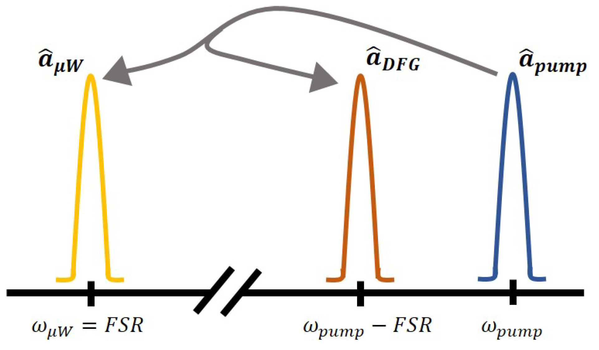
By suppressing or filtering out the SFG optical sideband, we are left with a triply-resonant system specialized for the generation of a microwave–optical photon entanglement, as shown in
Figure 1.
An example of this entanglement between microwave and optical fields at an mK range is presented in [
16]. There, a 2.5 mm radius, 150 μm thick ultra-low noise LiNbO
3 optical ring resonator was placed inside a superconducting microwave cavity at 7 mK. When the optical resonator is pumped by a laser and the momentum and energy conservation conditions
are satisfied, a spontaneous parametric downconversion process occurs, producing pairs of entangled optical and microwave photons. The non-classical correlations established between the microwave and optical modes were achieved through the co-localization and electro-optical coupling of the microwave mode with the optical whispering gallery modes, for which the microwave frequency was matched to the FSR of the resonator. This device is fully compatible with superconducting qubits but works at cryogenic temperatures. In addition, since the whispering gallery mode resonator (WGMR) used in [
16] is a 150 μm thick crystal, a system consisting of two gradient index lenses (GRINs) and a prism had to be used to couple the light into and out of the optical ring resonator, making the coupling mechanism complex and bulky.
Our goal is to develop an integrated device capable of creating entanglement between optical and microwave photons while taking advantage of photonic integration, thus eliminating the need for devices such as GRIN lenses and prisms.
2. Integrated Entanglement Generator
A novel structure for quantum entanglement generation, shown in
Figure 2, was designed and is currently at the fabrication stage. This device consists of two subsystems, optical and microwave, and is part of a LiNbO
3 photonic integrated circuit (PIC).
The optical subsystem is formed by a bus waveguide, a ring resonator, and an asymmetric Mach–Zehnder interferometer (AMZI). The bus waveguide facilitates the coupling of the optical pump required by the ring resonator to generate pairs of entangled microwave and optical photons. This coupling is achieved by evanescent field coupling between the bus waveguide and the cavity. However, due to the high-Q characteristic of LiNbO3 resonators, the operation bandwidth of the device will is limited by a few Megahertz (MHz). To overcome this limitation, a wavelength filter based on an asymmetric Mach–Zehnder interferometer is included to extract the optical photons in an overcoupled regime (wider resonance) while reinjecting the pump into the optical resonator.
The dimensions and layers of the microwave subsystem are specified in
Figure 3. This module consists of four main components: two half-wavelength resonators and two patch antennas. The half-wavelength resonators are fed independently and counter-phased by the patch antennas via microstrip lines. The resonators are realized by means of a circular slot around the LiNbO
3 ring resonator in the first metallization layer. In order to establish the boundary conditions of this type of resonator, i.e., the short-circuit terminations, two metal arcs are used in the second metallization layer, which are connected to the first metallization layer by vias.
Then, to provide an interface between the resonators and free space, two patch antennas are printed on the second metallization layer in a mirror configuration. The mirror configuration allows the RF system to simultaneously feed the resonators with a phase difference of 180°. The microwave system is responsible for emitting the entangled microwave photon generated within the WGMR.
The polarization of the antennas is linear along the Y axis as shown in
Figure 4, where the simulated realized gain reaches a maximum of −2.2 dBi. To test the system, two concentrated ports with a characteristic impedance of
were placed in the slots of the half-wavelength resonators just below the microstrip lines.
Before designing the entanglement generator, a passive PIC was developed to characterize the performance of the optical components involved in the generator. This first PIC was fabricated on a thin-film lithium niobate (TFLN) on an insulator platform and included the ring resonator and the AMZI. This paper presents the characterization results of this first PIC. These results were a key element in the design of the integrated device presented in
Figure 2.
Some of these experimental results have already been described in [
17], being the first study on the development of a photonic-based low-noise integrated radiometer. However, in this paper, we are interested in the development of a different device: an integrated entanglement generator that can also be used for microwave photon transmission and detection. Therefore, in addition to presenting the simulation results obtained in the design phase of the passive PIC and a more thorough study of the characterization results of the resonators and the asymmetric Mach–Zehnder interferometers, we also focus on the frequency stabilization of a laser to the integrated cavity to keep the optical wavelength always locked to a resonance of the resonator. By locking the laser to the WGMR, the intracavity power is increased, allowing for the generation of entangled microwave and optical photon pairs. Furthermore, although there are some similarities between the optical components used for the integrated radiometer and the integrated entanglement generator presented in this work, the microwave systems of the two PICs are completely different.
Since the PIC designed for entanglement generation is currently in the fabrication stage, this paper presents only the results of the characterization performed on the passive PIC.
3. Passive PIC Description
Lithium niobate is a non-centrosymmetric crystal that has large second-order nonlinear coefficients, a wide bandgap, and a relatively large refractive index (∼2.2 at 1550 nm), which allows for high-index-contrast waveguides to be formed on top of substrates like silicon dioxide (SiO
2). TFLN on an insulator has emerged as a promising material platform for different applications due to its large Pockels electro-optic efficiency [
18], low propagation loss, and high-Q on-chip ring resonators [
19].
The volume of the first PIC, which is 10 mm × 4 mm, is identified in
Figure 5. The figure also shows a microscopic image of the PIC where the two groups of structures under test can be observed. The first group consists of four AMZI devices, and the second group consists of eight single-coupled ring resonators.
Since we aimed to develop an integrated device for entangling microwaves with optical light, the characterization of integrated LiNbO3 ring resonators was relevant. The asymmetric Mach–Zehnder interferometers were included to test their functionality as wavelength filters for optical photon selection. Each group consisted of similar but not identical devices. The idea was to find the best-performing structure by varying the value of a design parameter between structures in the same group.
This passive PIC was fabricated using a 600 nm thick x-cut LiNbO
3 thin-film on 1.4 μm of SiO
2 as described in [
18]. The monolithic rib waveguides, whose cross-section is shown in
Figure 6a, characterized by a high index contrast and strong mode confinement, were fabricated by etching a total of 350 nm of LiNbO
3, resulting in a 250 nm thin LiNbO
3 slab. Losses of 2.7 ± 0.3 dB/m for straight waveguides and 9.3 ± 0.9 dB/m for bent waveguides were demonstrated in [
19].
For the AMZIs, an equal path length difference between their upper () and lower () arms of 250 μm was maintained in the four devices. However, the gap of the input and output directional couplers (DC) varied from structure to structure. It ranged from 0.65 μm in AMZI 1 to 0.35 μm in AMZI 4 in steps of 0.10 μm. By varying this parameter, it was possible to determine the fabrication characteristics of the DC to obtain a 50% splitting ratio. Each device had the same gap value for its input and output DC.
Regarding the resonators, all the structures had the same ring radius (50 μm) but different distances between the bus waveguide and the resonator. In this case, we were interested in studying the optical response of the integrated LiNbO3 resonators as a function of the waveguide/resonator gap. The different gap values were as follows: 1.4 μm (R1), 1.26 μm (R2), 1.11 μm (R3), 0.97 μm (R4), 0.829 μm (R5), 0.686 μm (R6), 0.543 μm (R7), and 0.4 μm (R8).
In the design phase, several simulations were performed to study the indices for the first guided mode of both TE and TM polarizations, as well as the bending loss as a function of the radius of curvature of the LiNbO3 waveguides. The simulations were carried out using the Finite Element Method (FEM) software (version 2021.09-2) from Synopsys (Sunnyvale, CA, USA).
To extract the bending loss, we performed a scan over the radius using MOST, a FemSIM function that uses a direct method to solve for bending modes. The direct method directly solves Maxwell’s equations in cylindrical coordinates without any approximation. For the fundamental TE mode, we obtained a straight waveguide and bending loss of
dB/m and
dB/m, respectively. For the fundamental TM mode, the straight and bent waveguide losses obtained were
dB/m and
dB/m, respectively. These simulation results are consistent with the low propagation losses presented by the platform in [
19].
The optical modes for waveguides with a width of 1.8 μm were obtained for both straight and bent configurations. The corresponding results are depicted in
Figure 6b for the straight waveguide and
Figure 6c for the bent waveguide.
To correctly analyze the transmission of thin-film LiNbO3 ring resonators, the dispersion characteristics of the guided modes must be considered. Since the effective index is wavelength-dependent due to two different properties, material and modal dispersion, we calculated the effective () and group () indices considering both properties.
Table 1 shows the
and
obtained for the fundamental TE mode in the straight and bent waveguides. The difference between the effective index and the group index is not negligible. Therefore, we must consider the influence of dispersion for a correct calculation of the FSR. The estimated FSR around
= 1550 nm for the TE mode is 3.8 nm considering the effective index and 3.33 nm working with
.
For the fundamental TM mode, we observe a similar behavior. The simulation results presented in
Table 2 show that the difference between the effective index and the group index is significant. The FSRs calculated with
and
are 3.96 nm and 3.23 nm, respectively.
4. Characterization Results
The devices were characterized using the component analyzer function of the high-resolution (0.08 pm) optical spectrum analyzer (BOSA) from Aragón Photonics (Zaragoza, Spain). The AMZI was characterized by first injecting the component analyzer tunable laser source (TLS) into the upper arm of its input DC and collecting the light from the upper (bar port) and lower (cross port) arms of the output DC. The input fiber was then switched to the lower arm of the input coupler, and the optical response was then recorded from the bar and cross output ports, which were then the lower and upper arms of the output coupler, respectively. In the case of the resonator, the characterization was simpler; the light injected into the input waveguide was collected from the output waveguide. In all measurements, the light was coupled into and out of the PIC via edge-coupled optical lensed fibers with a spot diameter of 2 μm. The insertion loss per facet was ∼5.5 dB.
4.1. Asymmetric Mach–Zehnder Interferometers
The light injected into one of the AMZI input ports is split by the first DC, resulting in two beams that experience different path lengths. This translates into a phase difference, so when the two beams are combined in the second DC, due to constructive and destructive interference, complementary optical powers are obtained at the output ports.
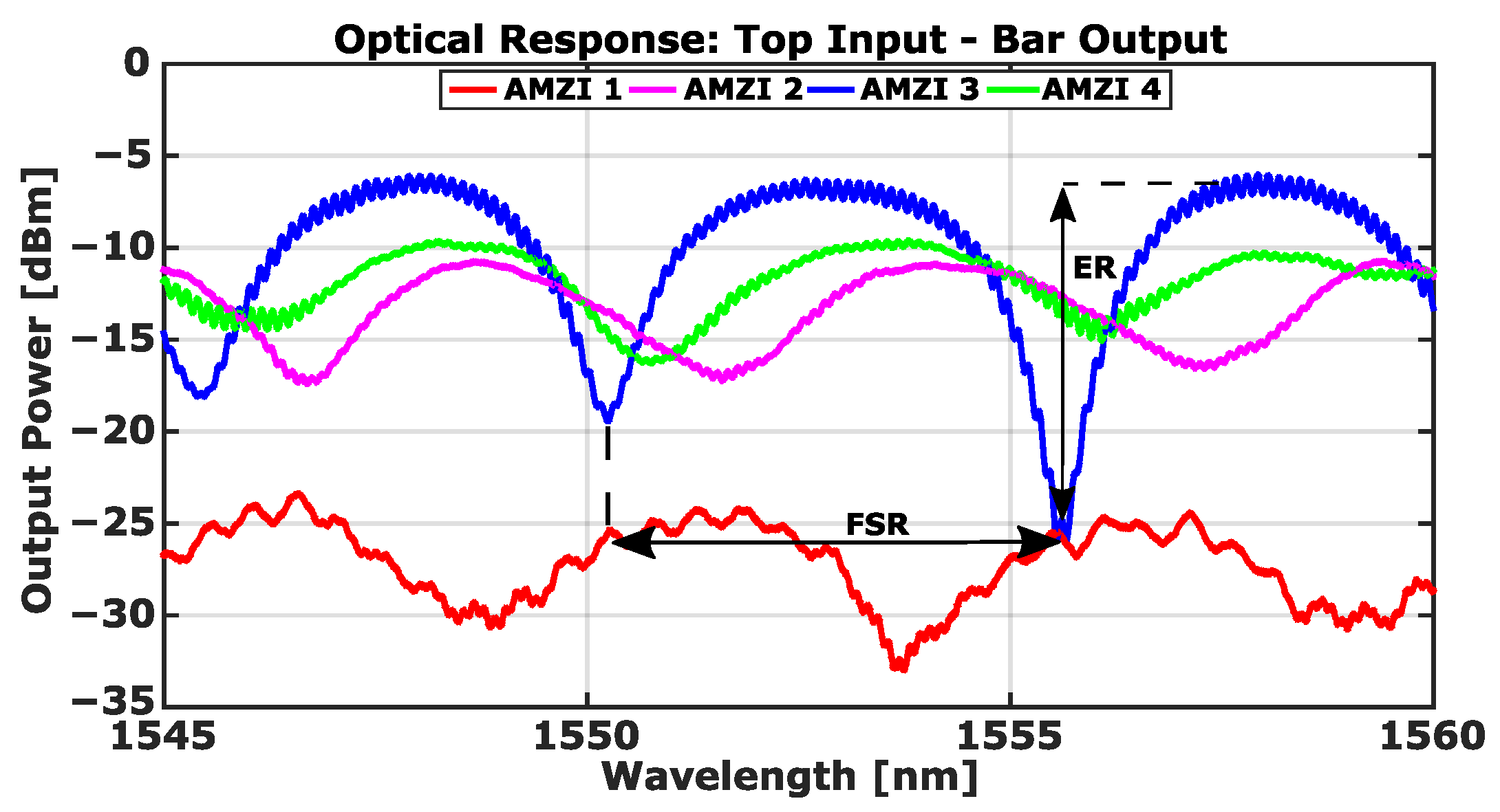
As mentioned above, the asymmetric Mach–Zehnder interferometer is used as an optical filter. Therefore, two figures of merit, identified in
Figure 7, must be studied, as well as the optical extinction ratio (ER) and the FSR. The ER is the ratio between the optical power at maximum and minimum transmissions, and the FSR is the distance, in optical wavelength, between two successive transmitted optical intensity minima.
Figure 7 and
Figure 8 show the response of the four asymmetric devices when the light is injected into the top arms of each input DC. The optical spectrum of the AMZIs, when the light is collected by the Bar output port (top arm of the output DC), can be seen in
Figure 7. In this scenario, the ERs measured in the devices are as follows:
dB (AMZI 1),
dB (AMZI 2),
dB (AMZI 3), and
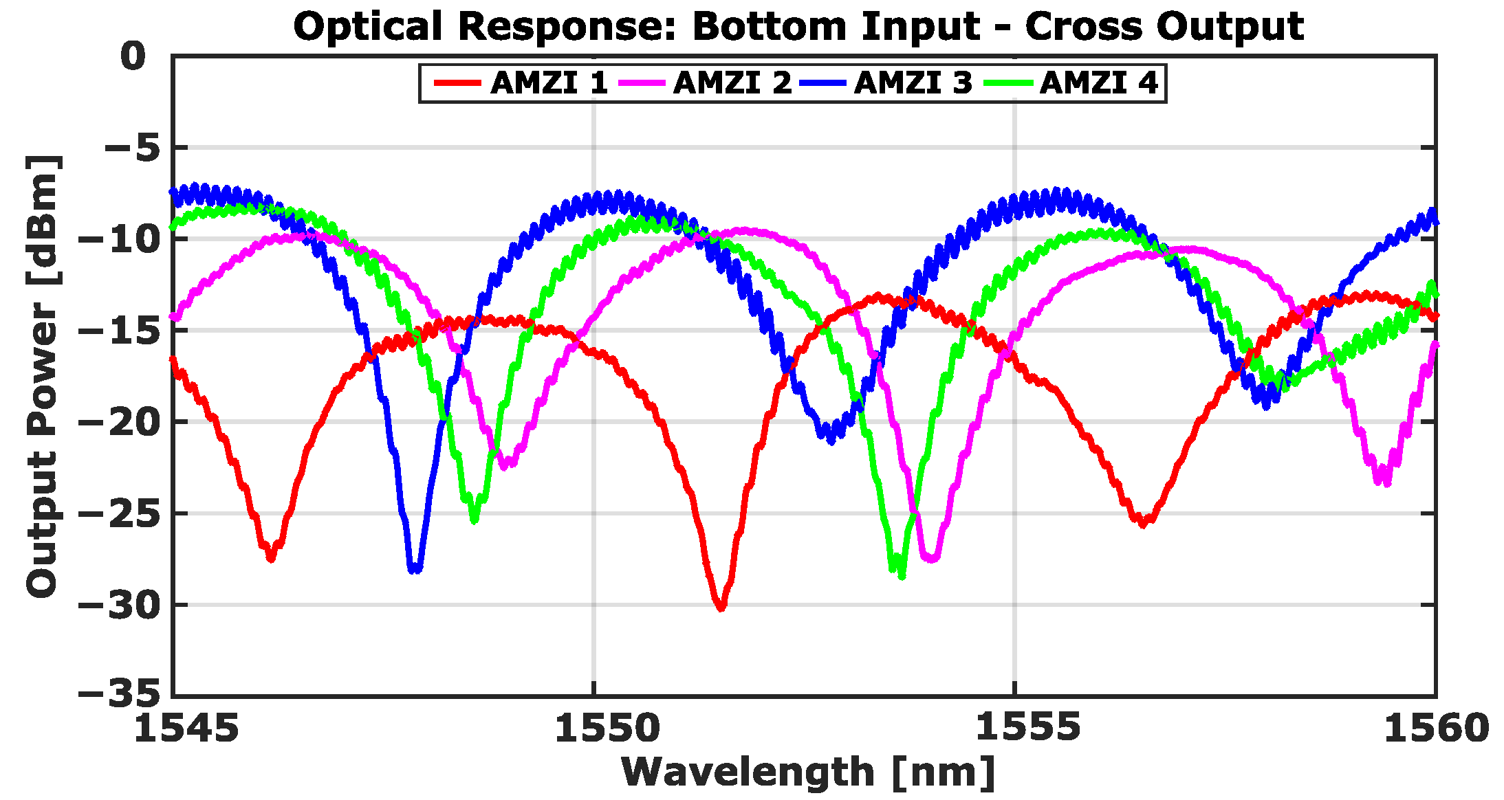
dB (AMZI 4). The optical spectrum of the structures, when recording the response from the Cross output port (bottom arm of the output DC), is shown in
Figure 8. The new values of the ERs are as follows:
dB (AMZI 1), 25 dB (AMZI 2), 25 dB (AMZI 3), and 13 dB (AMZI 4). From this first round of results, we can infer that, so far, the directional coupler gap that is more suitable for the design of a
DC is 0.45 μm since the highest ER at the Bar and Cross output ports is achieved with AMZI 3.
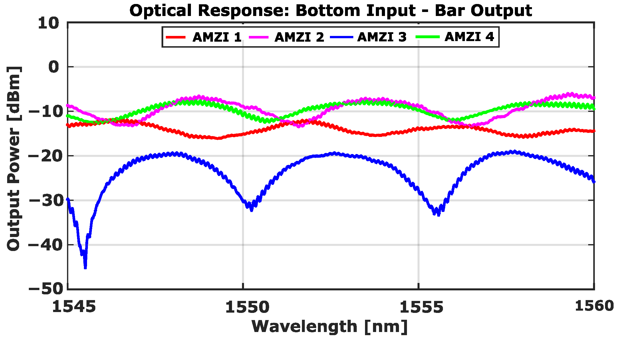
After this, the input fiber was changed to the bottom arm of the input directional coupler.
Figure 9 and
Figure 10 show the response of the four asymmetric devices when the light is collected from the top and bottom arms of the output DC, respectively. In this scenario, the ERs obtained at the Cross output port are as follows: 17 dB (AMZI 1), 18 dB (AMZI 2), 21 dB (AMZI 3), and 19 dB (AMZI 4). After collecting the light in this condition, the output fiber was moved to the bottom arm of the output directional coupler, and the resulting ERs were then as follows: 4 dB (AMZI 1),
dB (AMZI 2), 25 dB (AMZI 3), and 5 dB (AMZI 4).
To properly extract the value of the FSR from the transmission response of the asymmetric Mach–Zehnder interferometer, we have to consider that the wavelength spacing between the maximum and the minimum transmittance is defined by the path length imbalance (
) between the two arms of the AMZI as follows:
where
is the refractive index of the waveguides. The FSR is then given as
. For all four AMZI structures, as they were designed with the same
, the FSR was found to be around ∼5 nm (625 GHz).
As mentioned before, the different structures were designed and fabricated to calibrate the splitting ratio of the directional coupler as a function of the different gaps in order to find the optimum gap for the 50/50 coupler. From the value of the ERs, the splitting ratio of the directional coupler can be calculated as follows [
20,
21]:
where
is the normalized power obtained at the bar port of the directional coupler. The loss of the directional coupler is ignored.
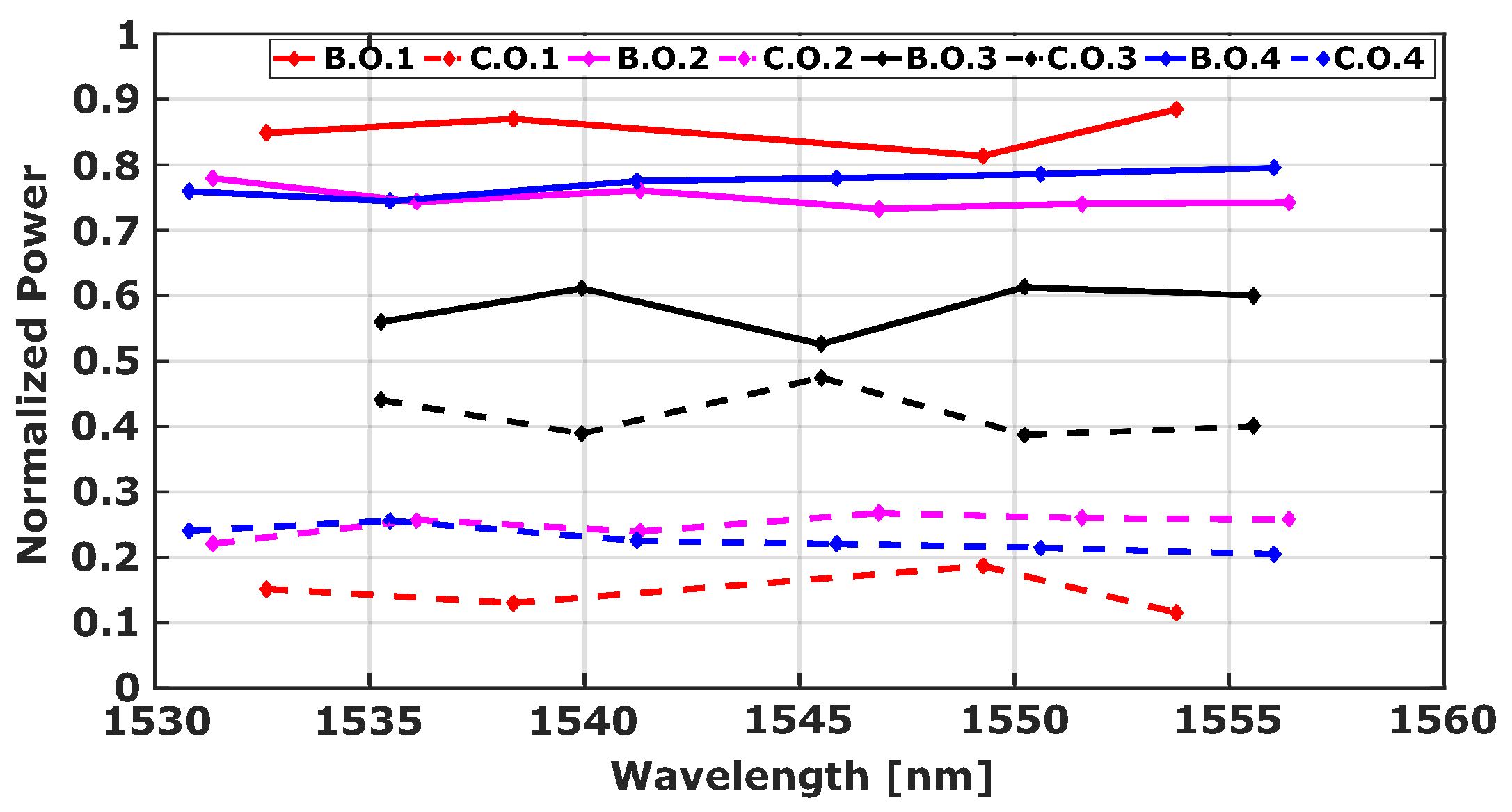
Figure 11 shows the calculated splitting ratios. The figure shows the power obtained at the Bar (B.O.) and Cross (C.O.) outputs of the coupler for each of the four structures.
From these results, we can affirm that the suppression of unwanted signals at each output port increases as the splitting ratio of the directional coupler approaches 50/50, and from all the results presented in this section, we can establish that the structure number 3 (0.45 μm) is the AMZI that provides the maximum suppression at both output ports when light is coupled to any arm of its input DC. Therefore, as shown in
Figure 11, its split ratio is closest to the expected 50%.
4.2. Ring Resonators
After testing the functionality of the Mach–Zehnder interferometers, we proceeded with the characterization of the second group of structures, the single-coupled resonators. As mentioned, the goal was to characterize the transmission response of the resonators as a function of the distance between the bus waveguide and the ring resonator.
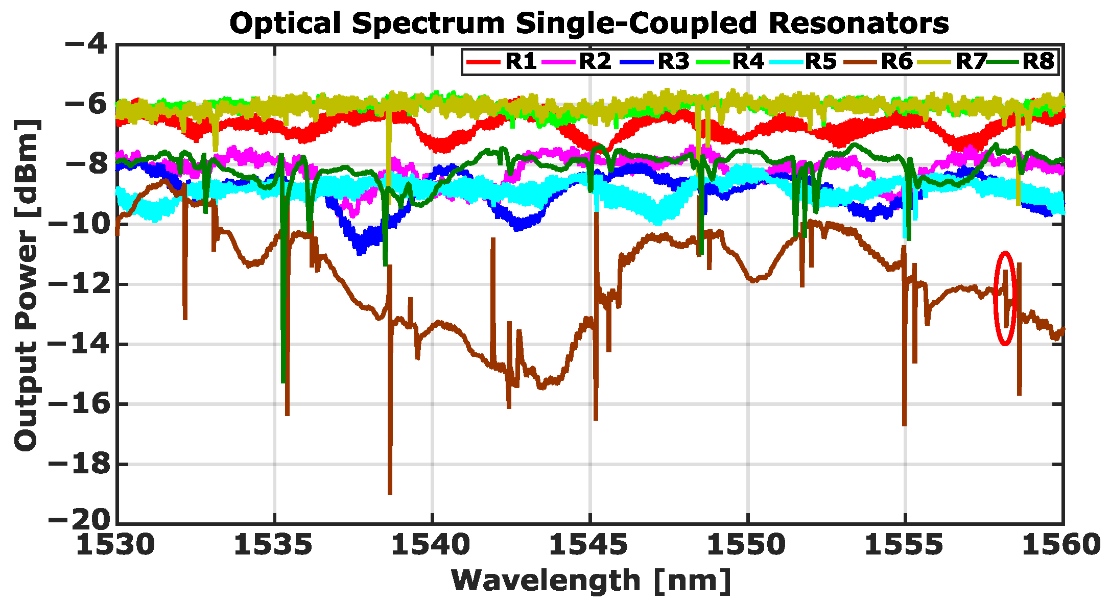
The transmission spectra of eight resonators are shown in
Figure 12. It can be observed that there are no resonances in the response of structures numbered 1, 2, 3, 4, and 5. This means that in our PIC, in order to observe coupling between the bus waveguide and the ring resonator, the maximum distance is limited to 0.7 μm.
A modulation of the optical spectrum is observed in all structures, resulting from the Fabry–Perot cavity created between the facets of the PIC, which can be reduced by using an anti-reflection coating on both edges of the chip. In the transmission spectrum of resonator number 6, we can also observe large amplitude oscillations due to reflections that occur at the fiber–waveguide interfaces when light is coupled in and out of the chip. These reflections are due to the difference in mode size between the lensed fibers used to couple the light in and out of the chip and the LiNbO
3 waveguides. In addition, some Fano resonances identified in
Figure 12 also appear in the spectrum of R6. The Fano-like shape is due to interference between the light coupled to the resonator and the reflected light, which leads to a perturbation of the phase of the transmitted wave [
22].
The resonance dips of resonators number 6, 7, and 8, at a wavelength of 1538 nm, are shown in
Figure 13. By fitting the experimental data of the resonators to a Lorentzian function, we can estimate the loaded quality factors (
), which are
,
, and
for R6, R7, and R8, respectively.
The intrinsic
Q-factor (
) of a ring resonator is related to the measured loaded Q-factor by the following:
where
is the normalized transmission value of the deep, and the +/− signs correspond to under- and over-coupled regimes, respectively.
At a critical coupling regime
, corresponding to an intrinsic
Q-factor of
. Therefore, with the measured quality factors, and through (Equation (
7)), the intrinsic quality factors extracted for R6, R7, and R8 are
,
, and
, respectively. From the quality factor of the integrated ring resonators, losses of around 2 dB/cm, 3.4 dB/cm, and 5.4 dB/cm are extracted for R6, R7, and R8, respectively. These values are a combination of propagation and bending losses.
Although the intrinsic Q-factors of the monolithically integrated LiNbO
3 ring resonators characterized in this work are high, they are not as good as state-of-the-art demonstrations on the same platform [
19]. This is due to the additional bending loss added by working with a smaller resonator radius.
The measured FSR was found to be ∼3.2 ± 0.2 nm (400 ± 25 GHz). Since the lithium niobate film thickness is smaller than the wavelength, the main contribution of dispersion to the FSR is given by the modal dispersion. Therefore, the measured FSR (3.2 ± 0.2 nm) is in correspondence with the theoretically calculated FSRs of nm and nm working with and , respectively. Thus, for the design of the optical ring resonator of the entanglement generator in the second PIC, we used .
4.3. Frequency Stabilization
As we mentioned before, the level of the optical signal inside the WGMR needs to be as high as possible to increase the probability of entanglement. Therefore, the laser has to be locked to a resonance of the ring resonator to avoid losing optical power. Then, the next step is to see if we can lock an external laser to one of our integrated resonators.
First, we used the component analyzer feature of BOSA to observe the transmission spectrum of the resonator (in this case, resonator number 7) and select the resonance at which the laser will be stabilized. A polarization controller was then used to maximize the resonance at 1561.85 nm. After selecting the resonance, we proceeded with the external laser injection. The optical wavelength was provided by a narrow-linewidth continuously tunable laser (CTL 1550) from Toptica. The scan amplitude and scan offset parameters of the laser were set to scan the optical wavelength in a range of 1 nm around the previously selected resonance.
The output of the PIC was then switched to the high-resolution optical spectrum analyzer port of the BOSA to display the laser wavelength after passing through the resonator. A 99:1 optical splitter was placed at the output of the PIC to observe the spectrum (1% signal) while injecting the signal (99%) into the photodiode (PD). The PD output was connected via a BNC-T connector to one of the inputs of the Toptica Pound–Drever–Hall (PDH) module for PDH locking, and to the Fine In 1 input on the front panel of the digital controller (DLC pro) to display the signal received from the PD and the lock point candidates. The PDH module of the DLC Pro contains the modulation and stages of the proportional-integral-derivative (PID) controller for the stabilization loop.
Figure 14 shows three different signal displays obtained by the Toptica application (TOPAS DLC pro) during the measurements.
The red signal is the input signal to the PDH module (output of the integrated ring resonator), the blue signal is the error signal generated by the module, and the lock point candidate is highlighted with a gray circle. In
Figure 14a, the PDH phase and modulation amplitude parameters were set to 109.3 and 2.8, respectively. After increasing both parameters to 115.7 and 12.8, respectively, a less noisy error signal was obtained, as can be seen in
Figure 14b. Finally, when the error signal resembles the derivative of the input signal, locking is achieved by tapping the candidate lock point and then pressing the Lock On/Off button.
When the laser is locked, the signal display looks like
Figure 14c, and the BOSA shows that the wavelength stabilizes at resonance. Note that due to high coupling losses, the error signal resembles only the derivative of the input signal around the resonance. The coupling losses should be reduced to obtain a stronger error signal.
5. Discussion
As mentioned in
Section 1, this research aims to develop an integrated device capable of generating entanglement between microwave and optical photons. The process is similar to the one described in [
16], with the added advantages of photonic integration, such as lower transmission losses, lower coupling losses, and a reduction in the size, weight, and power consumption (SWaP) of the device. To achieve this goal, we designed the integrated structure shown in
Figure 2, which is currently in the fabrication phase. The key elements are the LiNbO
3 WGMR and the microwave system. The resonator is responsible for the generation of entangled photon pairs, while the microwave system is responsible for the emission of the entangled microwave photon generated within the WGMR.
The use of a WGMR overcomes several challenges that can arise when conventional nonlinear materials are used directly in the entanglement generation process. By extending the interaction time, the WGMR enhances the nonlinearity, eliminating the need for a large crystal size to ensure an adequate interaction distance. The potential losses associated with the use of such a crystal are also reduced by the integrated approach presented in this paper. In addition, the use of this resonator structure enables the achievement of intracavity power levels that are orders of magnitude higher than the pump power [
13]. In addition, the proposed design of the integrated microwave system represents a significant reduction in both size and complexity compared to the conventional microwave cavities typically used for this purpose.
Unlike conventional receivers, which are practically perfect absorbers (and, thus, ideal sources of thermal noise), the WGMR is weakly coupled to a thermal bath due to its low level of absorption and radiation from the crystal, while in a bolometer, one tries to absorb as much energy as possible from the measured body; in the proposed scheme the opposite is true. In this system, low absorption is the optimal scenario, which means that the resonator is weakly coupled to the surrounding thermal bath. Consequently, the microwave signal modulates the optical carrier, appearing as sidebands, before the thermal noise can dominate the propagating microwave mode inside the crystal. According to a theoretical model presented in [
23], breaking the thermal equilibrium of counterpropagating whispering gallery modes (WGMs) occurs through overcoupling the microwave WGM. This results in the effective cooling of the upconverted mode, enabling room-temperature operation. In summary, a room temperature operation is achieved in this type of device because it is based on a passive cooling technique, as the noise and signals travel in opposite directions inside the LiNbO
3 ring resonator, and only the signal is extracted. Therefore, the effective noise temperature is lower than the physical temperature of the resonator [
13].
Although a room-temperature operation was also explained and discussed experimentally in [
23], the experimental system included multiple components, such as a gallium arsenide (GaAs) rod waveguide, a 5.66 mm diameter LiNbO
3 WGMR, and a diamond prism mounted on a piezoelectric stage, resulting in a device with high SWaP and complex experimental setup. In the new design presented here, this problem is solved through photonic integration.
6. Conclusions
In this paper, we present the initial stages of the development of a lithium niobate photonic integrated circuit for quantum applications. A novel integrated entanglement generator system, discussed in
Section 2, was designed and is currently under fabrication. In this work, we also report on the characterization results of monolithically integrated lithium niobate ring resonators and asymmetric Mach–Zehnder interferometers. These structures were integrated into a photonic integrated circuit for the first characterization of their functionalities, and the results obtained were used as a basis for the design of the second PIC, which incorporates a device developed for quantum entanglement, shown in
Figure 2.
The ring resonators showed a quality factor of about
, a value that is expected to increase in the current design by using Euler bends and increasing the radius of the ring (80 μm) in order to reduce the bending losses. Furthermore, another approach to increase the Q-factor by reducing losses is presented in [
24,
25]. By modifying the resonator geometry, the two main sources of radiation losses in the presence of curved waveguides—the discontinuities at the junctions between straight waveguides and the bent sections—can be mitigated.
For the AMZIs, a maximum ER of 25 dB was achieved in the structure with a DC gap of 0.45 μm. This ER value corresponds to a split ratio between 60 and 50 percent, which means that structure 3 offers a split ratio closer to the ideal 50/50. In addition, we succeeded in locking an external laser to the integrated ring resonator. This guarantees that any drift in the laser frequency can be corrected by the stabilization loop, preventing the system from experiencing an optical power loss within the WGMR.
