Article

Design Optimization of Silicon-Based Optically Excited Terahertz Wave Modulation

1
School of Physics and Optoelectronic Engineering, Beijing University of Technology, 100 Ping Le Yuan, Beijing 100124, China
2
Beijing Engineering Research Center of Precision Measurement Technology and Instruments, Beijing University of Technology, Beijing 100124, China
*
Author to whom correspondence should be addressed.
Photonics 2024, 11(3), 202; https://doi.org/10.3390/photonics11030202
Submission received: 28 January 2024 / Revised: 19 February 2024 / Accepted: 22 February 2024 / Published: 24 February 2024

Abstract

:
The modulation of a terahertz (THz) wave on amplitude, phase and polarization is important for the application of THz technology, especially in the field of imaging, and is one of the current research hotspots. Silicon-based, optically excited THz modulator is a wavefront modulation technique with a simple, compact and reconfigurable optical path. It can realize the dynamic modulation of THz wavefronts by only changing the projected two-dimensional pattern, but it still suffers from the problems of lower modulation efficiency and slower modulation rates. In this article, the Drude model in combination with the multiple thin layers structure model and Fresnel matrix method is used to compare the modulation efficiencies of three modulation modes and more factors. The method is more accurate than the popular proposed method, especially when the thickness of the excited photoconductive layers reaches a few hundred microns. In comparing the three modes, namely transmission, ordinary reflection and total internal reflection, it is found the total internal reflection modulation mode has the best modulation efficiency. Further, under this mode, the effects of three factors, including the lifetime of photo-excited carriers, the wavelength of pump light and the frequency of THz wave, on the performance of THz modulator are analyzed. The simulation results show that the realization of total internal reflection using silicon prisms is a simple and effective method to improve the modulation efficiency of a silicon-based optically excited THz modulator, which provides references for the design of a photo-induced THz modulator.

1. Introduction

Terahertz (THz) waves refer to electromagnetic waves with wavelengths between 30 μm and 3 mm and frequencies between 0.1 THz and 10 THz. THz waves have characteristic properties that are different from those of other electromagnetic bands; for example, THz waves are highly transparent to organic materials and most non-polar materials, and can be scanned and analyzed to obtain information on the composition and internal structure of the object to be measured. The low photon energy of THz waves also makes them ideal for non-destructive testing [1,2]. Moreover, THz waves have the property of being strongly absorbed by liquids and other states of water molecules, making them important in biomedical imaging applications [3,4]. In addition, because of their special position in the electromagnetic spectrum, which gives them the advantages of both microwave and infrared, THz also play a huge role in THz radar and communications [5,6].
With the rise of femtosecond laser technologies such as quantum cascade lasers [7] and new material detectors based on gallium arsenide Schottky diodes [8], THz technology is ready for further development, but the realization of active and efficient modulation of THz is still a challenge to be solved. Due to the low photon energy of THz waves, their response to most natural substances or materials is very weak. The current methods to realize effective modulation of THz radiation characteristics include carrier concentration modulation [9], liquid crystal modulation [10], phase change material modulation [11] and micro-electromechanical systems modulation [12]. In addition, metamaterials have important applications in the modulation of THz waves [13,14]. THz wave modulation technology based on semiconductor materials has achieved dynamic modulation of THz waves on amplitude, frequency, phase, polarization/polarization state and other parameters [15,16,17,18,19]. Especially in combination with digital micromirror devices (DMDs), THz waves are used to project two-dimensional patterns with a certain spatial distribution onto a semiconductor surface for photo-excitation to generate all-optical induced photoconductive patterns for wavefront modulation of THz. For example, T. Zhang et al. used a DMD to project an optically reconfigurable grating onto a thin silicon wafer with a thickness of 10 μm, obtaining enhanced TE polarized wave transmission in the THz band [20]. J. Guo et al. used a DMD to project a special illumination pattern onto an ultrathin silicon wafer, and formed a THz super-surface of subwavelength resonators of metal–silicon rod arrays on the silicon surface under the irradiation of a pump laser with an energy density of 140 μ J cm 2 ; this not only changed the phase distribution of the incident THz beam but also could be used for imaging [21]. In addition, B. Shams Itrat et al. used a Digital Light Processing (DLP) projector to project a Fresnel zone plate (FZP) onto a silicon wafer, and generated PI–FZPs to achieve focusing and steering of THz beams [22]. The modulation scheme of total internal reflection can further improve the modulation efficiency [23]. For example, X. Liu et al. proposed a triangular prism with a Quartz-Si-SiO2 structure, and it enhanced the attenuation efficiency of terahertz light by utilizing evanescent waves generated by total internal reflection and achieve close to 100% modulation in 12 mS [24]. R. I. Stantchev et al. used a laser diode with a central wavelength of 450 nm to project a Hadamard matrix pattern onto a silicon prism through the reflection of the DMD and three modulation geometries. Transmission, ordinary reflection and total internal reflection were studied, then the THz beam containing the object information was received by the detector through the total internal reflection of the silicon prism and, ultimately, acquisition of a THz video with 32 × 32 pixels at six frames per second [25].
When a semiconductor wafer is excited by pump light, the photo-excited carriers may diffuse inside it with a long distance (e.g., hundreds of micrometers). In this circumstance, Fresnel’s formula combined with impedance matching theory may no longer be applicable, since the infinitely thin photoconductive layer approximation becomes invalid. To better analyze the performance of a THz modulator of excited semiconductor wafer with a thickness of 500 μm, in this study, the Drude model in combination with the multiple thin layers structure model and Fresnel matrix method is used. The carrier concentration is calculated in each layer, taking into account carrier diffusion, and the Drude model is used to calculate the permittivity of each layer. Then the modulation efficiencies of three common modulation schemes, namely transmission, ordinary reflection and total internal reflection, are compared with each other. The effects of photo-excited carrier lifetime, pump light wavelength and THz frequency on the performance of a THz modulator under total internal reflection are investigated by simulation, which provides valuable references for the design of a photo-excited THz modulator based on semiconductor materials in terms of excitation light wavelength, incident terahertz wave frequency and choice of semiconductor material.

2. Principle of Silicon-Based Optically Excited THz Modulator

2.1. The Drude Model

Under high-energy laser excitation, assuming the incident laser photon energy h ν is higher than the semiconductor’s energy gap E g , some electrons of the semiconductor in the valence band will absorb the photon energy to migrate to the conduction band and become free electrons. At the same time, the same number of cavities will be generated in the valence band, generating electron–hole pairs. This results in the formation of nonequilibrium carriers near the semiconductor surface, i.e., photogenerated carriers, the concentration of which is proportional to the excitation light energy density; the principle is shown in Figure 1. The response of free carriers in semiconductors to THz radiation can be described by the Drude model [26], as shown in the following equation:
ε ˜ ( ω ) = ε b ω p 2 ω ( ω + i Γ ) ,
where ε ˜ ( ω ) denotes the relative complex dielectric constant of the excited semiconductor, ω is the excitation circular frequency, ε b is the background dielectric constant of the silicon, Γ is the damping rate, ω p = N q 2 ε 0 m * is the plasma frequency, N is the free carrier concentration, q is the electric charge, m * = ( 1 m e + 1 m h ) 1 is the free carrier effective mass and ε 0 ( ε 0 8.854 × 10 12   F / m ) is the vacuum dielectric constant.

2.2. The Complex Refractive Index of Excited High-Resistance Silicon

When the laser illuminates the semiconductor, the concentration of photogenerated carriers increases and the plasma frequency increases, which further leads to an increase in the complex conductivity of the semiconductor material and the formation of a transient photoconductive layer on its surface. When a THz wave is incident, the photoconductive layer additionally absorbs or reflects it, reducing the amplitude of the transmitted THz wave and thus realizing the modulation of the THz wave.
The recombination of photogenerated carriers within the semiconductor under laser irradiation can be described using the following equation [27,28]:
N e ( x , z , t ) t = g ( x , z , t ) r ( x , z , t ) + S e .
where the left side of the equation represents the variation of the photogenerated carrier concentration N , t represents the time, x is the spatial coordinates of the semiconductor surface, and z is the propagation distance of a THz wave inside the semiconductor perpendicular to its surface. The three terms on the right side of the equation represent the photogenerated carrier production, the recombination, and the diffusion process, respectively. Since the excitation light uniformly incidents on the surface of the semiconductor and its penetration depth within the semiconductor is much smaller than the width of the excitation region, the photogenerated carrier production rate g ( x , z , t ) can be approximated and simplified as:
g ( z , t ) = P ( 1 R e x ) α ω e x e α z ,
where P is the excitation optical power density, R e x is the reflectivity of the semiconductor substrate, α is the absorption coefficient, is the reduced Planck constant, and ω e x is the excitation circular frequency. A one-dimensional simplification of the steady state solution of the partial differential Equation (2) is obtained based on the photogenerated carrier concentration within the photo-excited semiconductor N e [29]:
N e ( z ) = τ e f f α P λ e x ( 1 R e x ) 2 π c ( 1 α 2 D e f f τ e f f ) [ e α z α 2 K B T μ e f f τ e f f q ( e z q 2 K B T μ e f f τ e f f ( 1 e ( α + q 2 K B T μ e f f τ e f f ) h 1 e 2 h q 2 K B T μ e f f τ e f f ) e z q 2 K B T μ e f f τ e f f ( 1 e ( α q 2 K B T μ e f f τ e f f ) h 1 e 2 h q 2 K B T μ e f f τ e f f ) ) ] ,
where τ e f f is the carrier lifetime, λ e x is the wavelength of the excitation light, c is the lightspeed, K B is Boltzman constant, D e f f is the carrier diffusion coefficient, T is the thermodynamic temperature, and h is the thickness of semiconductor silicon wafers. At this point, the total free carrier concentration in the semiconductor N is the sum of the photogenerated carrier concentration N e and the intrinsic carrier concentration N i , and N i is a constant value that has different values with different semiconductor materials.
After calculating the free carrier concentration according to the Drude model of Equation (1), the complex permittivity ε ˜ ( z , ω ) = ε Re ( z , ω ) + i ε Im ( z , ω ) corresponding to different positions at z within the semiconductor can be obtained, where ε Re ( z , ω ) and ε Im ( z , ω ) are the real and imaginary parts of the complex dielectric constant, respectively [30].
The complex refractive index n ˜ of a semiconductor satisfies the relationship between the relative complex permittivity ε ˜ ( z , ω ) is n ˜ 2 = ε ˜ ( ω ) and this gives the complex refractive index of THz waves at different locations within the semiconductor:
n ˜ ( z , ω ) = n ( z , ω ) + i κ ( z , ω ) ,
where
n ( z , ω ) = ε Re ( z , ω ) + ε Re 2 ( z , ω ) + ε Im 2 ( z , ω ) 2 ,
and
κ ( z , ω ) = ε Re ( z , ω ) + ε Re 2 ( z , ω ) + ε Im 2 ( z , ω ) 2 .
From the above equations, it can be seen the THz wave can be modulated in the amplitude and the phase distribution with the variety of n and κ , respectively, which is a hybrid modulation mode.

2.3. The Transmittance and Reflectance of THz Waves

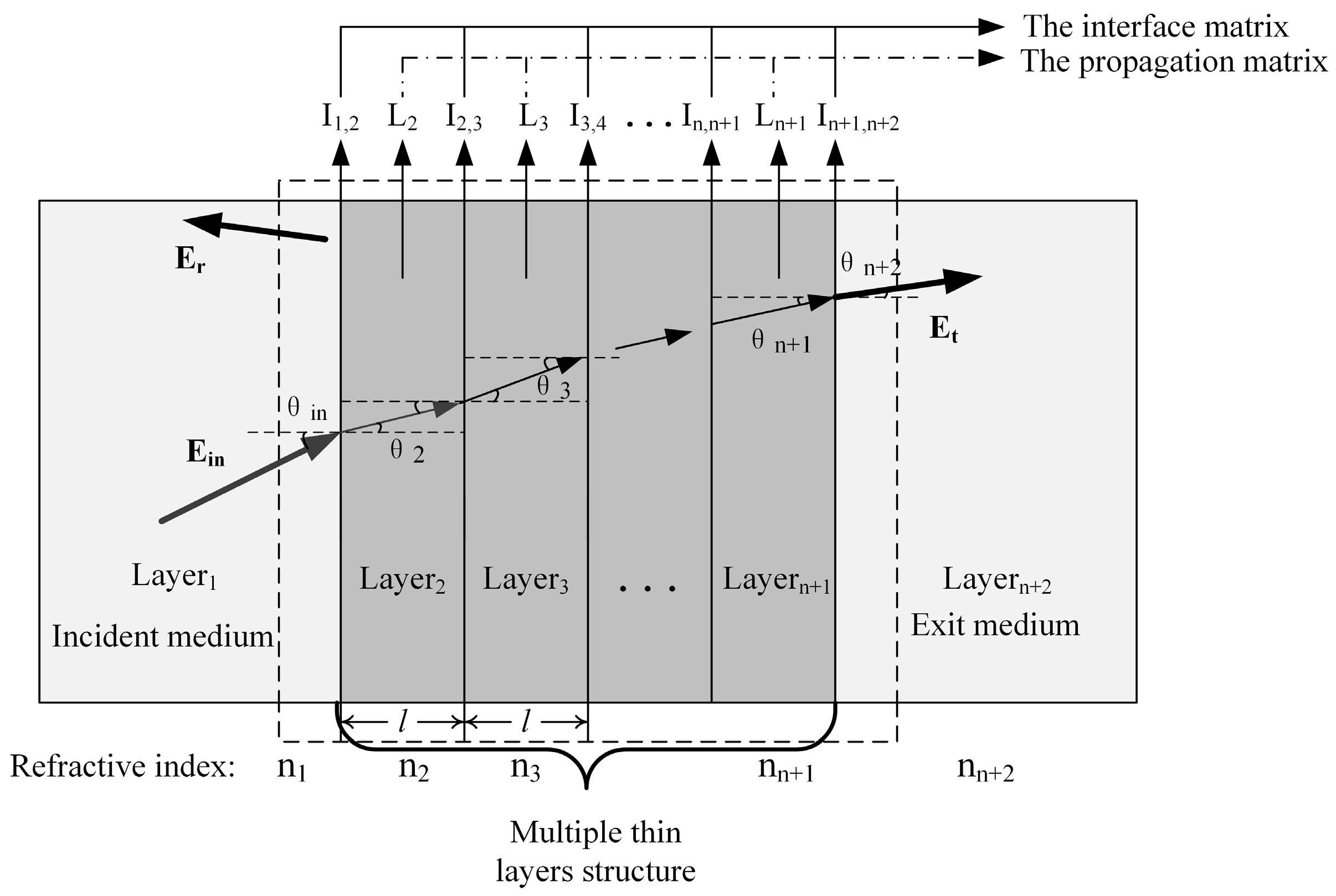
The carrier concentration in the semiconductor under optical excitation varies with the direction of THz wave incidence z in a gradient. At this time, the excited semiconductor is a non-uniform medium, and its complex refractive index is constantly changing with the propagation distance z . The semiconductor at this point can be regarded as a multilayer film structure consisting of a series of isotropic uniformly equal thickness parallel thin dielectric layers. The complex refractive index changes along the z-direction to satisfy the regularity of the film structure, and the transmittance or reflectivity of an incident THz wave can be calculated by combining it with the Fresnel matrix method. As shown in Figure 2, the THz propagation is effected by the interface matrix I j ( j + 1 ) at the interface between the two layers of medium and the propagation matrix L j in the same layer of medium, and they are expressed as follows [31]:
I j , ( j + 1 ) = 1 t j ( j + 1 ) 1 r j ( j + 1 ) r j ( j + 1 ) 1 ,
and
L j = e j φ j 0 0 e j φ j ,
where t j , ( j + 1 ) = 2 n j ˜ / ( n ˜ j + n ˜ j + 1 ) and r j , ( j + 1 ) = ( n ˜ j + 1 n ˜ j ) / ( n ˜ j + n ˜ j + 1 ) denote the Fresnel coefficients of THz waves at the interfaces of the jth and (j + 1)th thin dielectric layers, respectively. n ˜ j and n ˜ j + 1 are the complex refractive indices of the corresponding dielectric layers. φ j = 2 π l n ˜ j λ e x cos θ is the phase delay of the THz wave in the jth dielectric layer, l is the thickness of the dielectric layer, λ e x is the wavelength of the THz wave, and θ is the angle of incidence of THz waves passing through each dielectric layer. The scattering matrix of a THz wave passing through an excited semiconductor is expressed as:
S = I 1 , 2 L 2 I 2 , 3 L 3 L n + 1 I n + 1 , n + 2 = S 11 S 12 S 21 S 22 .
The transmittance (T) and reflectivity (R) of THz waves are calculated as:
T = 1 S 11 2 ,
and
R = S 21 S 11 2 ,

3. Simulation of a Silicon-Based Optically Excited THz Modulator

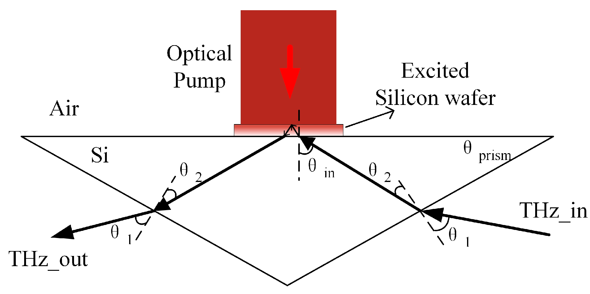
For a photo-excited THz modulator based on semiconductor silicon wafers, the generation of photogenerated carriers changes the complex refractive index of the silicon. It creates additional absorption and reflection of THz waves and thus achieves modulation of THz waves. All physical quantities affecting the concentration of the photogenerated carriers influence the performance of the modulator. A silicon prism-based photo-excited THz modulator is shown in Figure 3. A thin silicon wafer is placed on the upper surface of the silicon prism and closely fitted to it. The THz waves are incident from the air to the silicon prism and then pass through the silicon wafer. The reflection or transmission occurs at the interface between the surface of the silicon wafer and the air, and the propagation of THz waves in the excited silicon wafer is shown in Figure 2. The excitation light is incident from the upper side of the silicon wafer. As photogenerated carriers diffuse, THz waves undergo effective attenuation over longer distances within the semiconductor and therefore modulation efficiency is higher Due to the limited carrier diffusion distance, thicker semiconductors do not improve modulation efficiency, therefore here the thickness of the semiconductor silicon wafer was set to be 500 μm and divided into 40 layers, each of equal thickness. The incident THz wave frequency was set to 0.59 THz and the excitation wavelength was set to 808 nm; other parameters used in the simulation are shown in Table 1. For numerical simulations, the free carrier concentration N at the distance z from the semiconductor surface under different conditions (e.g., different excitation optical powers P , excitation optical wavelengths λ e x , incident terahertz wave frequencies f , etc.) is first calculated in conjunction with the Drude model by Equation (4), and then the complex permittivity ε ˜ ( z , ω ) and complex refractive index n ˜ ( z , ω ) of the excited semiconductor are calculated by Equations (5)–(7). According to the layering number of the multilayer thin structure, the transmission matrix I j , ( j + 1 ) and propagation matrix L j are calculated by Equations (8) and (9), respectively, and finally the scattering matrix S is obtained by cross dot multiplication to obtain the transmittance T and reflectance R of THz waves at this time by Equations (10)–(12).
The performance of the THz modulator is characterized using the modulation depth MD, which is defined as shown in Equation (13). T ( R ) n o   p u m p i n g and T ( R ) p u m p i n g denotes the THz wave transmittance or reflectivity when the semiconductor is not excited and is excited, respectively.
M D = T ( R ) n o   p u m p i n g T ( R ) p u m p i n g T ( R ) n o   p u m p i n g .
The variation of complex permittivity ε ˜ and complex refractive index n ˜ at different locations within the semiconductor is observed using the above parameters, and the results are shown in Figure 4. As the THz propagation distance continues to increase, the real part of the complex permittivity and complex refractive index of silicon decreases and the imaginary part increases. This indicates that along the direction of THz wave propagation the concentration of photogenerated carriers gradually increases, and the greater the degree of excitation of silicon, the greater the loss to THz waves.
Based on the previous theoretical analysis, this article first analyzes the modulation efficiency of three common modulation geometry schemes through simulation, then analyzes the effects of the photogenerated carrier lifetime τ e f f within the semiconductor, the excitation light wavelength λ e x , and the incident THz wave frequency f on the performance of the modulator.

3.1. The Transmittance and Reflectance of THz Waves

As shown in Figure 3, a silicon prism was used to observe the transmittance T of THz waves at different angles of incidence θ i n . The excitation optical power density P was set to 0.5 W / c m 2 . The excited semiconductor silicon sheet was placed on a silicon prism and fitted closely to it, and the angle of incidence θ i n satisfies the following relation:
θ i n = arcsin ( n A i r sin θ 1 n S i ) + θ p r i s m .
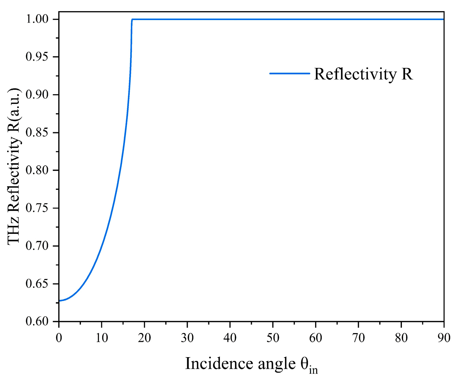
where n A i r and n S i are the refractive indices of air and silicon, which are set to 1 and 3.42, respectively, and θ p r i s m is the base angle of the silicon prism. Considering the excited silicon wafer as a multilayer film structure, with each layer of equal thickness and the refractive index varying with the concentration of diffused photogenerated carriers, the reflection angle of a terahertz wave at the wafer–air interface is related to the angle of incidence. The simulation results are shown in Figure 5, from which it can be seen that total internal reflection occurs when the angle of incidence θ i n = 18 . As the excitation optical power density P continues to increase to 1 W / c m 2 , the silicon sheet is excited to difference degrees, the refractive index will change, and the critical angle of total internal reflection increases slightly, but not more than 1 .
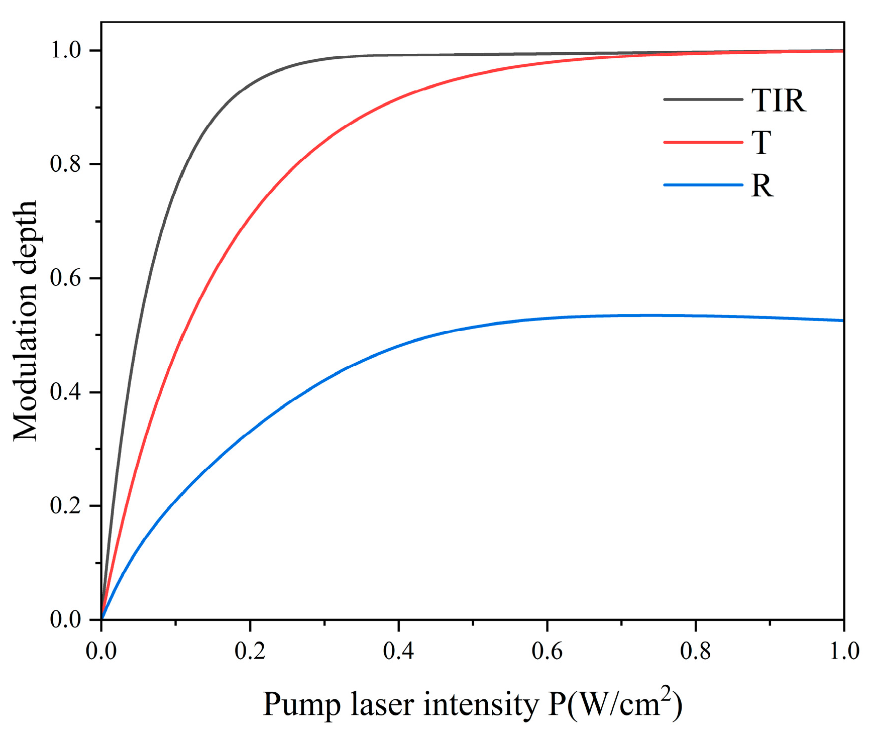
Based on the above analysis, to ensure that the total internal reflection occurs and the angle of incidence θ i n is set to 30 in subsequent simulations, the incidence angle of transmitted and normally reflected THz waves θ i n is set to 8.5 , and the excitation optical power density P is varied to observe the changes in the modulation depth of transmitted, ordinary reflected and total internal reflection; the results are shown in Figure 6. From the simulation results, it can be found that the modulation depth M D of the THz modulator under the three common modulation schemes gradually increases with the increasing excitation optical power. For normal reflection and total internal reflection, M D increases to 1 when P increases to 0.765 W / c m 2 and 0.35 W / c m 2 , respectively. As P continues to increase, MD remains constant. For transmission, when P increases to 0.615 W / c m 2 , M D increases to the maximum value of 0.53. Of the three common modulation geometry schemes, the total internal reflection modulation is the most efficient for the same excitation optical power density. The realization of total internal reflection using silicon prisms is a very simple, effective and feasible scheme to improve the performance of a silicon-based, optically excited THz modulator. The subsequent simulations are based on the modulation geometry scheme of total internal reflection.

3.2. The Influence of Different Physical Parameters on the Performance of THz Modulator

  • Photogenerated carrier lifetime
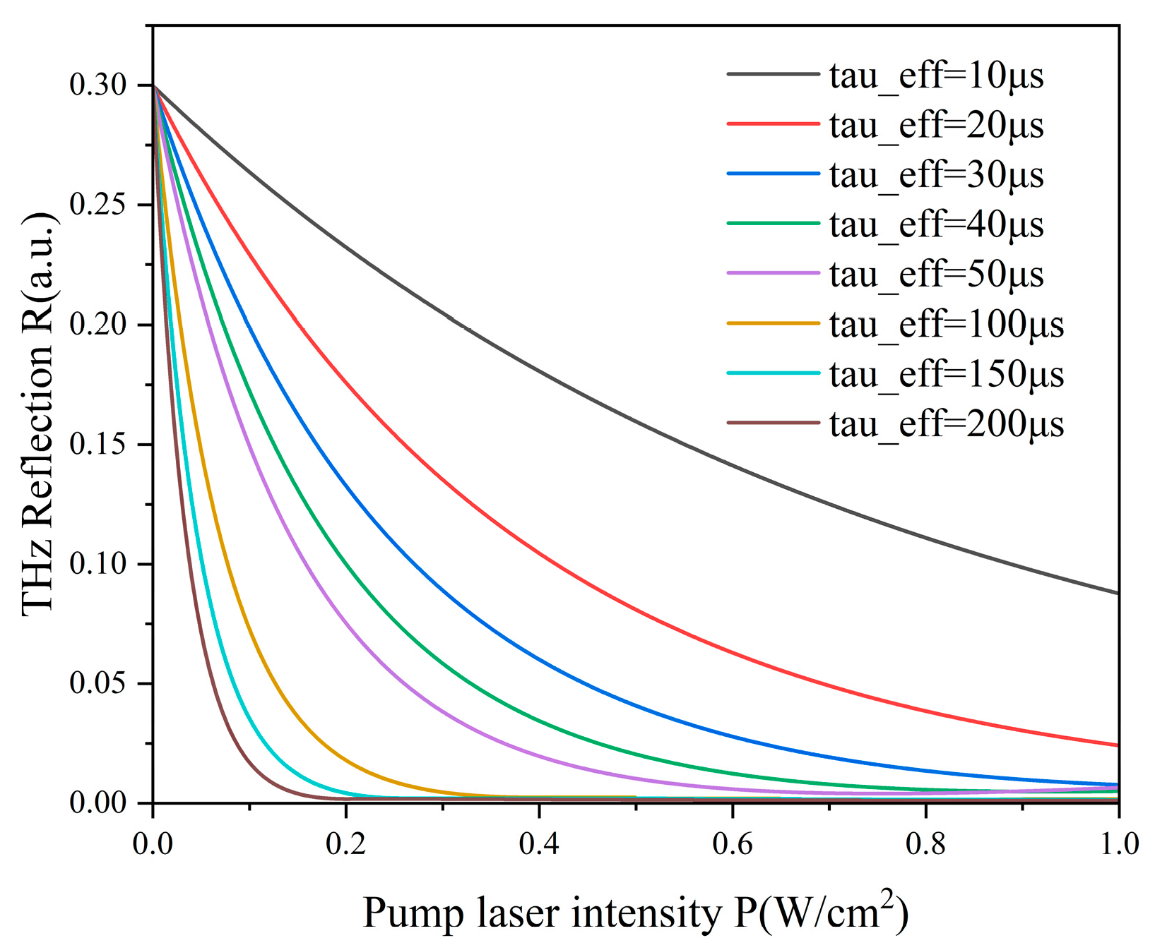
The results of the variation of the reflectivity of THz waves with increasing excitation optical power at different carrier lifetimes are shown in Figure 7. It can be seen from the simulation that the longer the lifetime of the photogenerated carriers, the faster the reflectivity R of the THz wave decreases, which means that the lower the excitation optical power P required when the reflectivity R decreases to 0, and the higher the modulation efficiency of THz waves. At τ eff of 100 μ s , 150 μ s and 200 μ s , the excitation optical power required to minimize R is 0.393 W / c m 2 , 0.329 W / c m 2 , and 0.214 W / c m 2 , respectively. Therefore, semiconductor materials with longer photogenerated carrier lifetimes can be chosen, or carrier complexation rates can be reduced by coating semiconductor surfaces with heterogeneous films to enhance their lifetime and thereby improve modulation efficiency.
2.
Excitation light wavelength
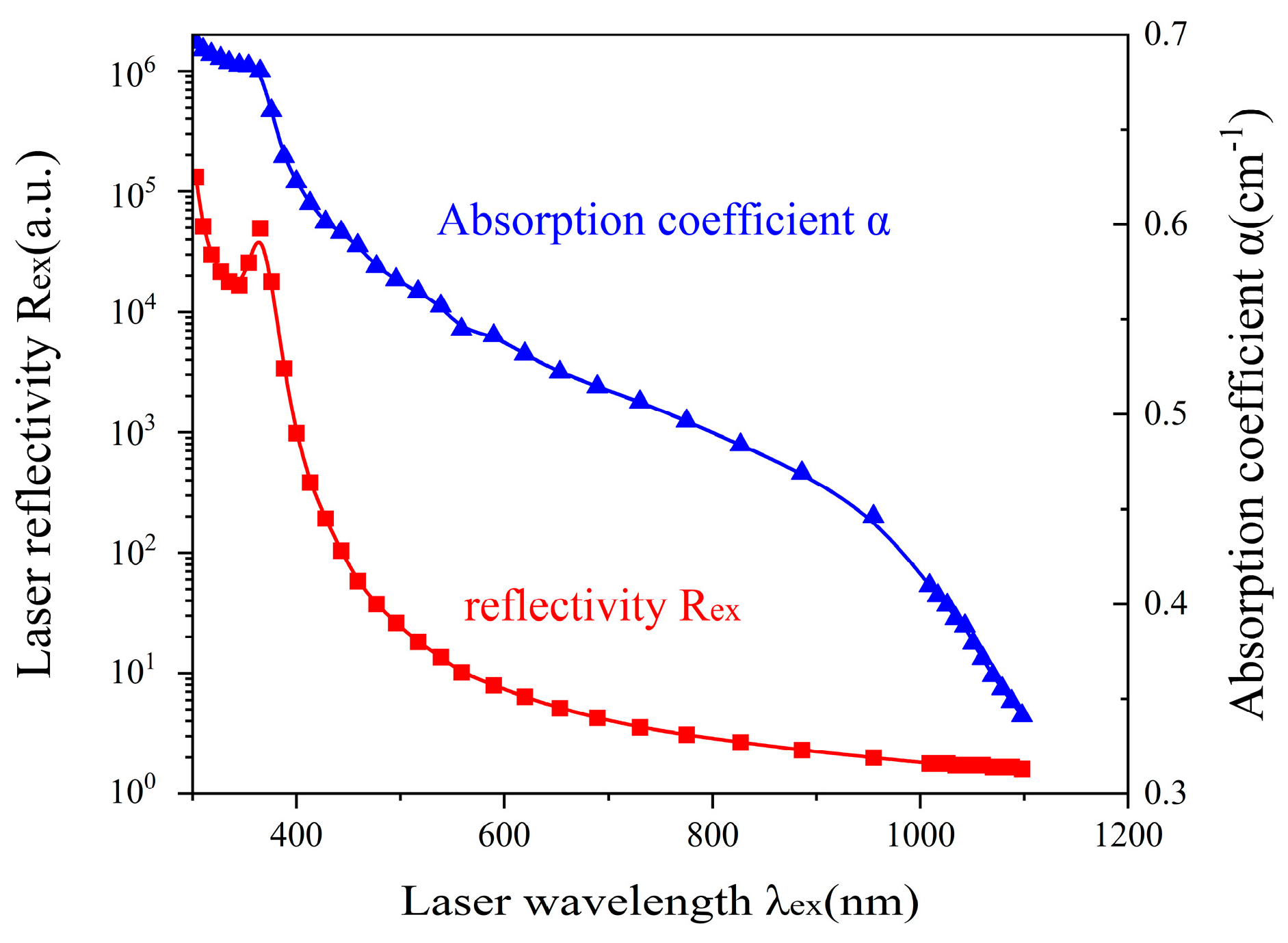
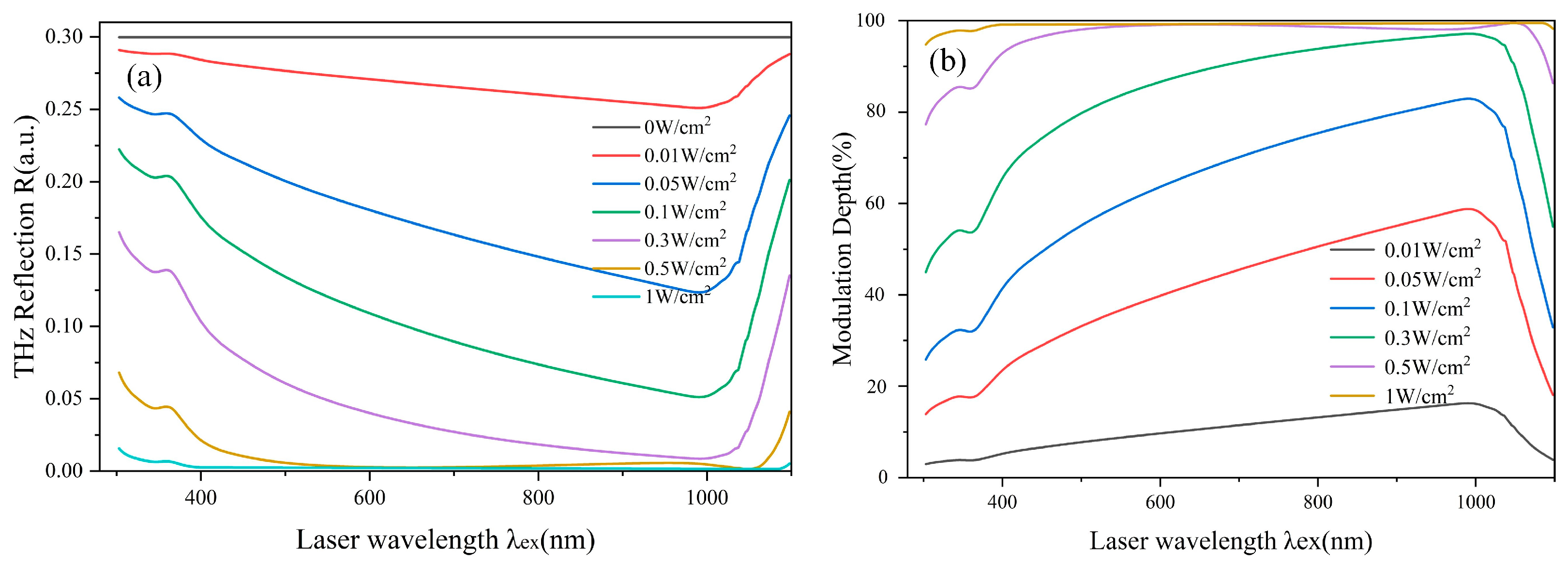
According to Equation (3), it can be seen that changing the excitation light wavelength directly affects the generation of photogenerated carriers. At the same time, with different wavelengths of excitation light, the absorption coefficient α and reflectivity R e x of silicon also change, thus affecting the generation of photogenerated carriers, which in turn has an impact on the performance of the THz modulator. Figure 8 shows the absorption coefficient α and reflectance R e x of silicon at different excitation light wavelengths [32]. Figure 9a shows the variation of THz wave reflectivity R for different excitation wavelengths and power densities P. Figure 9b shows the variation of MD for different excitation wavelengths λ e x and power densities P. It can be seen that with the increasing excitation optical power, the THz reflection R will show the characteristic of decreasing firstly and then increasing rapidly. The MD is above 95% when the laser optical power is 0.5 W / c m 2 and the excitation light wavelength λ e x is between 421 nm and 1080 nm.
3.
Incident THz wave frequency
The incident THz frequency was varied to observe its effect on the performance of the THz modulator, and the results are shown in Figure 10. As the excitation optical power increases, the reflectivity R of the THz wave gradually decreases and the modulation depth gradually increases at the same time, which means the modulation efficiency increases. With the increasing frequency of the incident THz wave, the reflectivity R keeps increasing, and both MD and modulation efficiency gradually decrease.

4. Conclusions and Discussion

In this study, when the semiconductor light-excited THz modulators has a thick excited semiconductor measuring 500 μm, the performance of the THz modulator is simulated using the Drude model in conjunction with the multiple thin layers structure model and the Fresnel matrix method. Firstly, the modulation efficiencies of three common modulation geometries, namely transmission, ordinary reflection and total internal reflection, are compared. The simulation results show that under the same excitation optical power, the modulation efficiency of total internal reflection is the highest, followed by transmission, and ordinary reflection is the lowest. Secondly, the effects of photo-excited carrier lifetime τ e f f , pump light wavelength λ e x , and incident THz wave frequency f on the performance of THz modulator during total internal reflection were investigated by simulation. The results show that the longer the carrier lifetime, the higher the modulation efficiency. Under the conditions of the excitation light power of 0.5 W / c m 2 , pump light wavelength ranges between 421~1080 nm, and the modulation depth can reach more than 95%. The lower the incident THz frequency, the higher the modulation efficiency. The semiconductor-based photo-excited THz modulator is a simple, compact and reconfigurable technology for optical paths. Total internal reflection using silicon prisms is a very efficient, feasible and compact solution to improve the performance of a silicon-based optically excited THz modulator.
The main methods to enhance the MD of semiconductor optically excited THz modulators include using high-power excitation light sources, construction of metallic resonant structures on semiconductor surfaces and preparation of thin nanolayers on semiconductor surfaces to form composite structures. The proposed method uses silicon prisms in combination with total internal reflection to realize modulation of the THz wave, which has simple structure and higher MD (close to 100%). We will further verify this by conducting additional experiments in the future.

Author Contributions

C.Z.: Methodology, Software, Writing-original draft. D.W.: Methodology, Data curation, Writing-review and editing, Supervision, Funding acquisition. J.Z.: Methodology, Data curation, Writing-review and editing. L.R.: Formal analysis. Y.W.: Formal analysis. S.L.: Formal analysis. All authors have read and agreed to the published version of the manuscript.

Funding

National Natural Science Foundation of China (62220106005, 62075001, 62175004, 62275006); Natural Science Foundation of Beijing Municipality (4222061, 4222063).

Institutional Review Board Statement

Not applicable.

Informed Consent Statement

Not applicable.

Data Availability Statement

Data underlying the results presented in this paper are not publicly available at this time but may be obtained from the authors upon reasonable request.

Conflicts of Interest

The authors declare no conflicts of interest.

References

  1. Zhong, H.; Redo-Sanchez, A.; Zhang, X.-C. Identification and classification of chemicals using terahertz reflective spectroscopic focal-plane imaging system. Opt. Express 2006, 14, 9130–9141. [Google Scholar] [CrossRef] [PubMed]
  2. Yamashita, M.; Kawase, K.; Otani, C.; Kiwa, T.; Tonouchi, M. Imaging of large-scale integrated circuits using laser terahertz emission microscopy. Opt. Express 2005, 13, 115–120. [Google Scholar] [CrossRef] [PubMed]
  3. Son, J.H. Principle and applications of terahertz molecular imaging. Nanotechnology 2013, 24, 214001. [Google Scholar] [CrossRef] [PubMed]
  4. Fan, S.; He, Y.; Ung, B.S.; Pickwell-MacPherson, E. The growth of biomedical terahertz research. J. Phys. D-Appl. Phys. 2014, 47, 374009. [Google Scholar] [CrossRef]
  5. Vamsi, C.S.; Dwivedi, A.K.; Bharti, G.; Verma, V.R.; Sharma, A. Efficient graphene-based circularly polarized MIMO antenna for THz applications. Appl. Opt. 2022, 61, 8155–8161. [Google Scholar] [CrossRef] [PubMed]
  6. Kleine-Ostmann, T.; Nagatsuma, T. A review on terahertz communications research. J. Infrared Millim. Terahertz Waves 2011, 32, 143–171. [Google Scholar] [CrossRef]
  7. Wang, X.; Shen, C.; Jiang, T.; Zhan, Z.; Deng, Q.; Li, W.; Wu, W.; Yang, N.; Chu, W.; Duan, S. High-power terahertz quantum cascade lasers with ~0.23 W in continuous wave mode. AIP Adv. 2016, 6, 075210. [Google Scholar] [CrossRef]
  8. Mehdi, I.; Siles, J.V.; Lee, C.; Schlecht, E. THz diode technology: Status, prospects, and applications. Proc. IEEE 2017, 105, 990–1007. [Google Scholar] [CrossRef]
  9. Stantchev, R.I.; Phillips, D.B.; Hobson, P.; Hornett, S.M.; Padgett, M.J.; Hendry, E. Compressed sensing with near-field THz radiation. Optica 2017, 4, 989–992. [Google Scholar] [CrossRef]
  10. Savo, S.; Shrekenhamer, D.; Padilla, W.J. Liquid crystal metamaterial absorber spatial light modulator for THz applications. Adv. Opt. Mater. 2014, 2, 275–279. [Google Scholar] [CrossRef]
  11. Zhang, Y.; Qiao, S.; Sun, L.; Shi, Q.W.; Huang, W.; Li, L.; Yang, Z. Photoinduced active terahertz metamaterials with nanostructured vanadium dioxide film deposited by sol-gel method. Opt. Express 2014, 22, 11070–11078. [Google Scholar] [CrossRef]
  12. Herrmann, E.; Gao, H.; Huang, Z.; Sitaram, S.R.; Ma, K.; Wang, X. Modulators for mid-infrared and terahertz light. J. Appl. Phys. 2020, 128, 140903. [Google Scholar] [CrossRef]
  13. Kowerdziej, R.; Jaroszewicz, L. Active control of terahertz radiation using a metamaterial loaded with a nematic liquid crystal. Liq. Cryst. 2016, 43, 1120–1125. [Google Scholar] [CrossRef]
  14. Ramachandran, T.; Faruque, M.R.I.; Islam, M.T.; Khandaker, M.U.; Alqahtani, A.; Bradley, D.A. Development and Analysis of Coding and Tailored Metamaterial for Terahertz Frequency Applications. Materials 2022, 15, 2777. [Google Scholar] [CrossRef] [PubMed]
  15. Lee, G.; Maeng, I.; Kang, C.; Oh, M.-K.; Kee, C.-S. Strong polarization-dependent terahertz modulation of aligned Ag nanowires on Si substrate. Opt. Express 2018, 26, 13677–13685. [Google Scholar] [CrossRef] [PubMed]
  16. She, R.; Liu, W.; Wei, G.; Lu, Y.; Li, G. Terahertz single-pixel imaging improved by using silicon wafer with SiO2 passivation. Appl. Sci. 2020, 10, 2427. [Google Scholar] [CrossRef]
  17. Wu, X.; Pan, X.; Quan, B.; Wang, L. Optical modulation of terahertz behavior in silicon with structured surfaces. Appl. Phys. Lett. 2013, 103, 121112. [Google Scholar] [CrossRef]
  18. Kamaraju, N.; Rubano, A.; Jian, L.; Saha, S.; Venkatesan, T.; Nötzold, J. Subcycle control of terahertz waveform polarization using all-optically induced transient metamaterials. Light-Sci. Appl. 2014, 3, e155. [Google Scholar] [CrossRef]
  19. Guan, S.; Cheng, J.; Chang, S. Recent progress of terahertz spatial light modulators: Materials, principles and applications. Micromachines 2022, 13, 1637. [Google Scholar] [CrossRef]
  20. He, J.W.; Wang, X.K.; Xie, Z.W.; Xue, Y.Z.; Wang, S.; Zhang, Y. Reconfigurable terahertz grating with enhanced transmission of TE polarized light. APL Photonics 2017, 2, 076102. [Google Scholar] [CrossRef]
  21. Guo, J.; Wang, T.; Zhao, H.; Wang, X.; Feng, S.; Han, P.; Sun, W.; Ye, J.; Situ, G.; Chen, H.; et al. Reconfigurable terahertz metasurface pure phase holograms. Adv. Opt. Mater. 2019, 7, 1801696. [Google Scholar] [CrossRef]
  22. Shams, I.B.; Jiang, Z.; Rahman, S.M.; Cheng, L.-J.; Hesler, J.L.; Fay, P.; Liu, L. A 740-GHz dynamic two-dimensional beam-steering and forming antenna based on photo-induced reconfigurable Fresnel zone plates. IEEE Trans. Terahertz Sci. Technol. 2017, 7, 310–319. [Google Scholar] [CrossRef]
  23. Sun, Q.; Chen, X.; Liu, X.; Stantchev, R.I.; Pickwell-MacPherson, E. Exploiting total internal reflection geometry for terahertz devices and enhanced sample characterization. Adv. Opt. Mater. 2020, 8, 1900535. [Google Scholar] [CrossRef]
  24. Liu, X.; Parrott, E.P.J.; Ung, B.S.-Y.; Pickwell-MacPherson, E. Exploiting total internal reflection geometry for efficient optical modulation of terahertz light. APL Photonics 2016, 1, 076103. [Google Scholar] [CrossRef]
  25. Stantchev, R.I.; Yu, X.; Blu, T.; Pickwell-MacPherson, E. Real-time terahertz imaging with a single-pixel detector. Nat. Commun. 2020, 11, 2535. [Google Scholar] [CrossRef] [PubMed]
  26. Georgiou, G.; Tyagi, H.K.; Mulder, P.; Bauhuis, G.J.; Schermer, J.J.; Rivas, J.G. Photo-generated THz antennas. Sci. Rep. 2014, 4, 3584. [Google Scholar] [CrossRef]
  27. Vogel, T.; Dodel, G.; Holzhauer, E.; Salzmann, H.; Theurer, A. High-speed switching of far-infrared radiation by photoionization in a semiconductor. Appl. Opt. 1992, 31, 329–337. [Google Scholar] [CrossRef]
  28. Wilson, T.E. Modeling the high-speed switching of far-infrared radiation by photoionization in a semiconductor. Phys. Rev. B 1999, 59, 12996. [Google Scholar] [CrossRef]
  29. Kannegulla, A.; Bin Shams, I.; Liu, L.; Cheng, L.-J. Photo-induced spatial modulation of THz waves: Opportunities and limitations. Opt. Express 2015, 23, 32098–32112. [Google Scholar] [CrossRef]
  30. Ulbricht, R.; Hendry, E.; Shan, J.; Heinz, T.F.; Bonn, M. Carrier dynamics in semiconductors studied with time-resolved terahertz spectroscopy. Rev. Mod. Phys. 2011, 83, 543. [Google Scholar] [CrossRef]
  31. Born, M.; Wolf, E. Principles of Optics; Cambridge University: Cambridge, UK, 1999. [Google Scholar]
  32. Liu, L.; Xiao, Q.; Xu, H.; Schultz, J.C.; Lichtenberger, A.W.; Weikle, R.M. Design, Fabrication and Characterization of a Submillimeter-Wave Niobium HEB Mixer Imaging Array Based on the “Reverse-Microscope” Concept. IEEE. Trans. Appl. Supercond. 2007, 17, 407–411. [Google Scholar] [CrossRef]
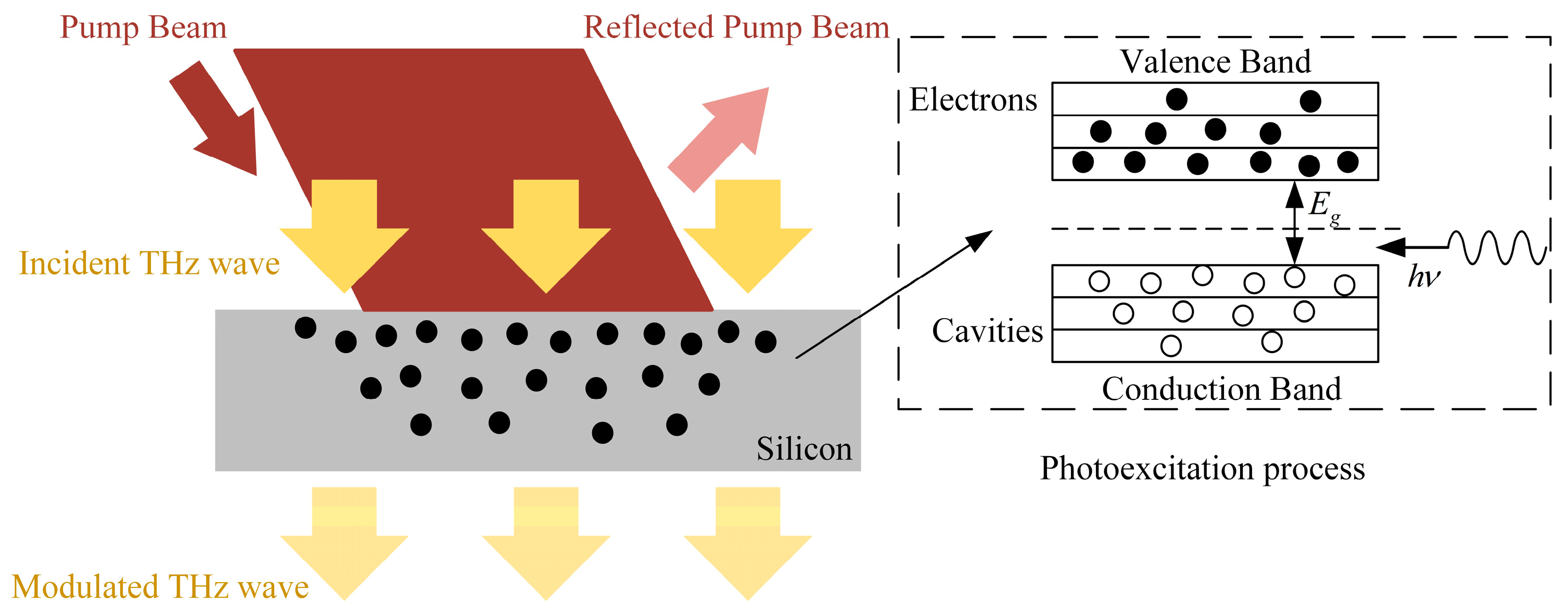
Figure 1. Principles of silicon-based optically excited THz wave modulation. When the photon energy of the pump light is greater than the band gap of silicon, electron–hole pairs are generated near the surface to form photogenerated carriers diffusing inside, then THz waves are additionally absorbed or reflected and thus modulated.
Photonics 11 00202 g001
Figure 2. Calculation of THz wave transmittance or reflectance using the multilayer thin layers structure model combined with the Fresnel matrix method. The thickness of each film in the multiple structure is equal, and the refractive index is constantly changing. THz waves have different angles of θ i n and θ o u t at each layer of the medium and satisfy Snell’s Law.
Photonics 11 00202 g002
Figure 3. Schematic of a silicon prism-based THz modulator. The pump light incidents from above to excite the silicon wafer, changing its refractive index distribution. When THz waves incident at an angle θ 1 to the silicon prism and enter its top thin silicon wafer, the total internal reflection occurs at the interface between the upper part of the thin silicon wafer and the air.
Photonics 11 00202 g003
Figure 4. Variation of complex permittivity and complex refractive index of excited silicon thin film with propagation distance z. (a) Variation of the real and imaginary parts of the dielectric constant. (b) Variation of the real and imaginary parts of the complex refractive index.
Photonics 11 00202 g004
Figure 5. The reflectivity of terahertz spatial light modulators at different angles of incidence θ i n .
Photonics 11 00202 g005
Figure 6. Comparison of modulation depth at transmission, ordinary reflection and total internal reflection.
Photonics 11 00202 g006
Figure 7. Variation of terahertz wave reflectivity with excitation optical power density for different carrier lifetimes.
Photonics 11 00202 g007
Figure 8. Variation of absorption coefficient α and reflectance R e x of silicon at different excitation light wavelengths.
Photonics 11 00202 g008
Figure 9. Variation of reflectivity and MD of THz waves with wavelength for different excitation optical power densities. (a) Variation of THz wave reflectivity R. (b) Variation of modulation depth MD.
Photonics 11 00202 g009
Figure 10. Variation of THz wave reflectivity and MD with incident THz wave frequency for different excitation optical power densities. (a) Variation of THz wave reflectivity R. (b) Variation of modulation depth MD.
Photonics 11 00202 g010
Table 1. Some of the parameters used in the simulation and their values.
ParametersValuesParametersValues
Carrier lifetime of silicon τ eff 100 μ sReduced Planck constant 1.05457266 × 10 34   J · S
Intrinsic carrier concentration N i 1.45 × 10 10   c m 3 Excitation optical power density P 0 1   W / c m 2
Absorption coefficient α 1.013 × 10 3   c m 3 Reflectivity R e x 0.329
Thermodynamic temperature T 293.15 KBoltzman constant K B 1.38064 × 10 23
Electron mobility μ e 1500   c m 2 / V s Hole mobility μ h 450   c m 2 / V s
Electron effective mass m e 0.26 m 0 Hole effective mass m h 0.38 m 0
Dielectric constant ε b 11.7Diffusion coefficient D e f f 17.31   c m 2 / s
Disclaimer/Publisher’s Note: The statements, opinions and data contained in all publications are solely those of the individual author(s) and contributor(s) and not of MDPI and/or the editor(s). MDPI and/or the editor(s) disclaim responsibility for any injury to people or property resulting from any ideas, methods, instructions or products referred to in the content.