1. Introduction
The ever-increasing demand for ultra-low latency and enhanced data throughput necessitates the advancement of data communication systems toward higher transmission capacity. The inherent bandwidth limitations of electronic components, when compared to their photonic counterparts, act as a bottleneck for pushing the transmission capacity towards extremely high data rates, not to mention the electronics’ susceptibility to electromagnetic interferences, time jitter, and resistive-capacitive delays. This highlights the critical importance of high-performance interface building blocks responsible for inter-domain conversion, such as digital-to-analog converters (DACs), which convert digital signals into analog ones. While conventional electronic DACs commonly deploy interleaving solutions to deal with the speed (i.e., conversion rate) and resolution trade-off [
1], photonic-based implementations of DACs provide promising alternative solutions with improved conversion rates and efficiency, attracting a multitude of research directions from the summation of weighted wavelength division multiplexed (WDM) signals to segmented Mach-Zehnder Modulators (MZMs) driving methods [
2,
3,
4,
5,
6,
7,
8,
9,
10,
11,
12,
13,
14,
15,
16,
17,
18,
19,
20]. This interest extends beyond addressing the above bandwidth limitations, encompassing the realization of high-performance DACs for instrumentation, arbitrary waveform generation [
21], photonic parallel processing [
22], and other potential domains.
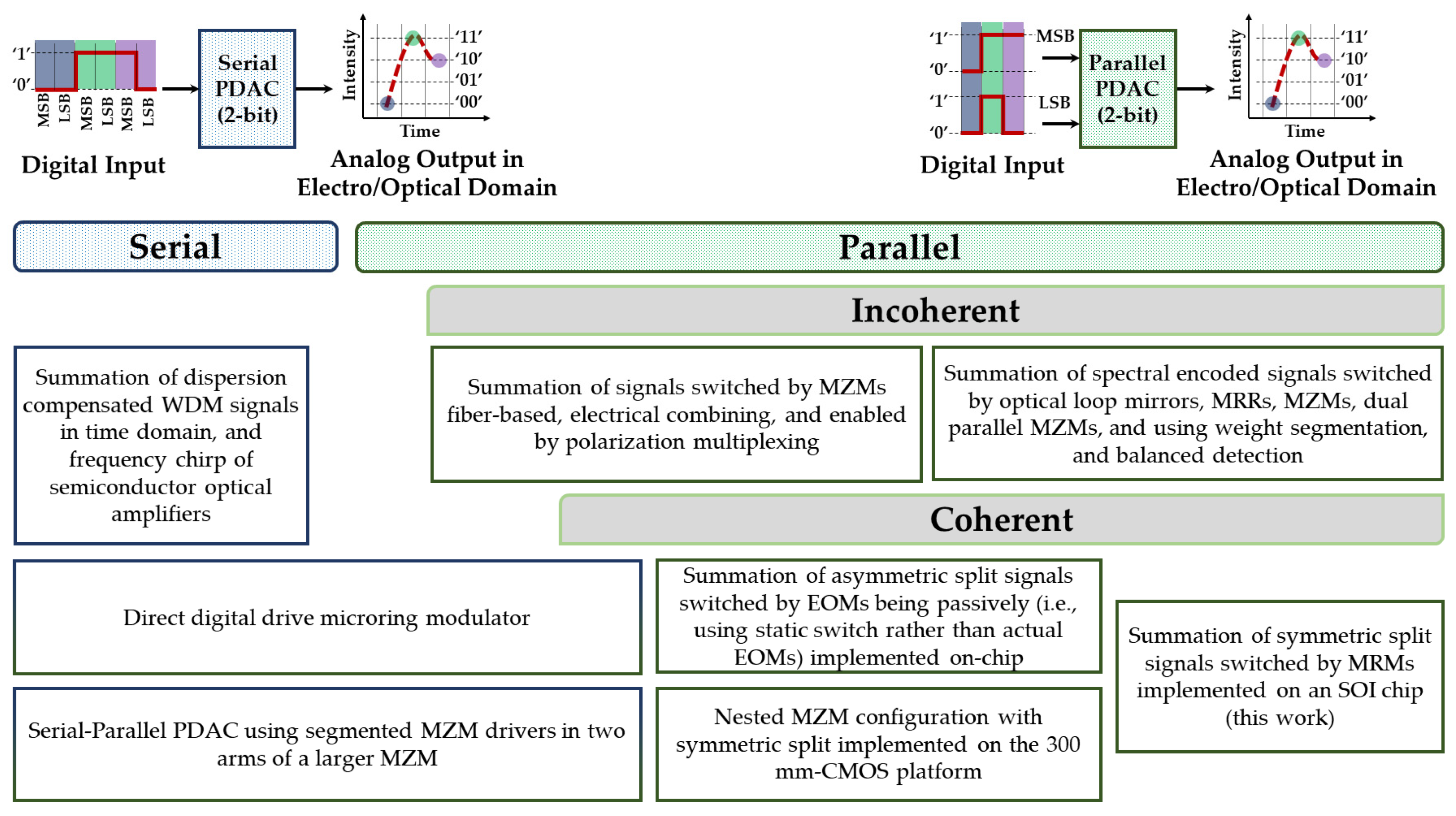
Photonic implementation of DAC requires the representation of numerical values with commensurate light intensities. The state-of-the-art photonic DAC (PDAC) topologies are roughly categorized into serial and parallel schemes, as depicted in
Figure 1. Serial photonic DACs, as the name implies, utilize a serial methodology for converting digital input into analog signals using optical technology. This usually involves the summation of weighted multiwavelength pulses that are precisely spaced in the time domain by the deployment of the dispersion phenomenon [
2,
3]. The multiwavelength pulses are assigned specific weights and are then passed through a dispersive medium to ensure they remain separated in time and preserve the correct amplitude. This technique, also known as photonic time-stretch technology, makes the modulated signal stretched in the time domain and overlapped among different wavelength bands to realize incoherent summation [
4]. A similar methodology is proposed in [
5] by the deployment of the frequency chirp feature of the semiconductor optical amplifiers, also known as blue-chirp spectral slicing. In general, serial PDACs trade-off bit resolution for conversion rate, meaning that they may not be able to provide high bit resolution at high sampling rates. Furthermore, attaining the output analog signal in these topologies depends on a wide-band opto-electro conversion at the output because each intensity level consists of several signals with different wavelengths. In other words, only an analog electronic signal is attainable at the output, which limits their applicability in case a photonic analog signal is desired.
It is worth noting that a PDAC could be also realized by the
n-bit driving of a single modulator (e.g., an electro-absorption or a microring modulator). The downside of this approach is the additional overhead requirement of a bulky and power-hungry electronic DAC (EDAC) for the
n-bit driving of the modulator, making this scheme a less appealing solution as an EDAC alternative. The power consumption of typical 8-bit EDACs ranges from 0.56 to 4.03 W for 60 to 100 GS/sec sampling rates, respectively [
23,
24]. Nevertheless, a direct-digital-drive approach could alleviate the need for additional EDACs, to some extent, despite the demand for a digital memory lookup table to deal with non-linearity issues [
6]. This topology, loosely classified under both serial and parallel categories, encounters technical challenges when the PDAC resolution is scaled up because of the trade-off between the inherently finite resonance extinction ratio of microring modulators and the overhead of the scheme dealing with the non-linear power transmission.
Parallel PDACs offer an excellent solution to the conversion rate limitations by using multiple parallel channels and allowing for higher conversion rates and higher bit resolutions. The basic idea of parallel PDACs relies on the incoherent or coherent summation of binary switched-weighted signals. The weighting operation is predominantly conducted by splitting the monotone input signal through cascaded symmetric or asymmetric splitters. Past works in the field, such as references [
7,
8], are two examples of off-chip fiber-based implementation of the first proposed PDACs. They proposed using a large-area photodetector (PD) and a wide-band incoherent optical input source (i.e., erbium-doped fiber amplifier), respectively, to realize an incoherent summation of signal paths switched by MZMs. Quite similarly in [
9], the authors utilized another solution for realizing an on-chip incoherent summation objective, which is using a PD at the end of each weighted signal path and performing the summation in the electronic domain, sacrificing the footprint and bandwidth to avoid coherent summation. Using a polarization multiplexing scheme, the work reported in [
10] proposed a 2-bit PDAC switched by a dual-polarization modulator. Furthermore, another class of incoherent parallel PDACs employs spectral weight encoding of the multiwavelength optical signal using nonlinear optical loop mirrors [
11], microring resonators (MRRs) [
12,
13], MZMs [
14], and dual parallel MZMs [
15]. The incoherent summation resolution in this class could be improved with a novel quantization scheme enabled by a weight segmentation and balanced detection approach, as introduced in [
16,
17]. In this class, not only does the incoherent output summation depends on spectral PD accumulation, but it also demands optical sources at multiple wavelengths that can affect the overall power efficiency of the system, not to mention the requirements of having the same conversion time for each wavelength.
In the work of [
18], they proposed a coherent scheme based on switching an intensity-weighted optical by employing electro-optic modulators (EOMs). Cascaded asymmetric directional couplers provide intensity weighting of the input monotone optical signal to be further switched by EOMs according to the digital input signal. Unlike incoherent parallel PDACs, the technical challenge of the coherent scenario is that the phase mismatch between the paths deteriorates stable intensity summation, degrading the signal-to-noise ratio that can lead to scalability limitations. Hence, a phase shifter is deployed on each signal path to support the in-phase coherence of signals before being summed up by the Y-junction combiners. The proof-of-principle design reported in [
18] in the silicon-on-insulator (SOI) platform demonstrated the switching of each signal path in a passive manner without utilizing actual EOMs and hence deployed a simulation methodology to calculate the performance metrics of the design. In addition, the fabrication sensitivity of the deployed asymmetric directional couplers and Y-junctions significantly deteriorates a desirable yield in terms of the linearity performance of the PDAC. In comparison, the authors of [
19] proposed using a nested MZM configuration employing symmetric splitters/combiners for both intensity weighting and output combining. The actual chip is fabricated on a 300 mm-CMOS platform to be able to accommodate a large footprint of MZMs. Recently, the work of [
20] introduced a novel architecture combining both serial and parallel schemes by employing a segmented MZM configuration in conjunction with 90° phase shifters specifically designed for applications in quadrature amplitude modulation (QAM) and pulse-amplitude modulation (PAM) schemes. Despite the potential conceptual advancement, the practical implementation of this architecture remains unexplored, not to mention the relatively huge footprint requirements of MZMs hindering the resolution scalability of such topology.
By comparing the serial and parallel schemes, it is evident that the conversion rate of the parallel scheme is N times larger than the serial scenario at the same modulator speed and bandwidth (N being the resolution). Furthermore, it is important to note that almost all of the state-of-the-art serial and parallel incoherent PDAC topologies, unlike coherent ones, rely on photodetectors to generate the desired analog intensity, thereby limiting the scope of their application. These applications, such as photonic parallel processing, all-optical machine learning, and optical telecommunication, to name a few, necessarily require the analog signal to be in the optical domain. This is also suitable for high-speed operations as it does not involve the conversion latency of the photodiodes, and the speed is mainly determined by the modulator bandwidth. On the other hand, the inherent challenge of coherent topologies is that all modulated signals of the parallel channels must be added coherently. This can be addressed by the deployment of additional phase shifters, while not affecting the overall power efficiency when the optical path length difference is minimized by the design.
In this work, we propose and experimentally demonstrate a parallel coherent PDAC architecture utilizing symmetric multimode interference couplers (MMIs) and ring resonator-based modulators. MMIs enable a balanced weighting and combining scheme that is more robust to fabrication process variation compared to state-of-the-art architectures [
18,
19]. Switching each signal path by MRMs provides an ultra-compact and power-efficient solution compared to the related work based on MZMs [
19]. We discuss the deployed tuning strategy to realize coherent summation functionality. The experimental testbed enabling dynamic digital-to-analog conversion with 2-bit resolution is also provided. Different from the approach in [
18], this work experimentally implements the modulation functionality using MRMs. Further simulation results support the potential of this approach for realizing higher conversion rates.
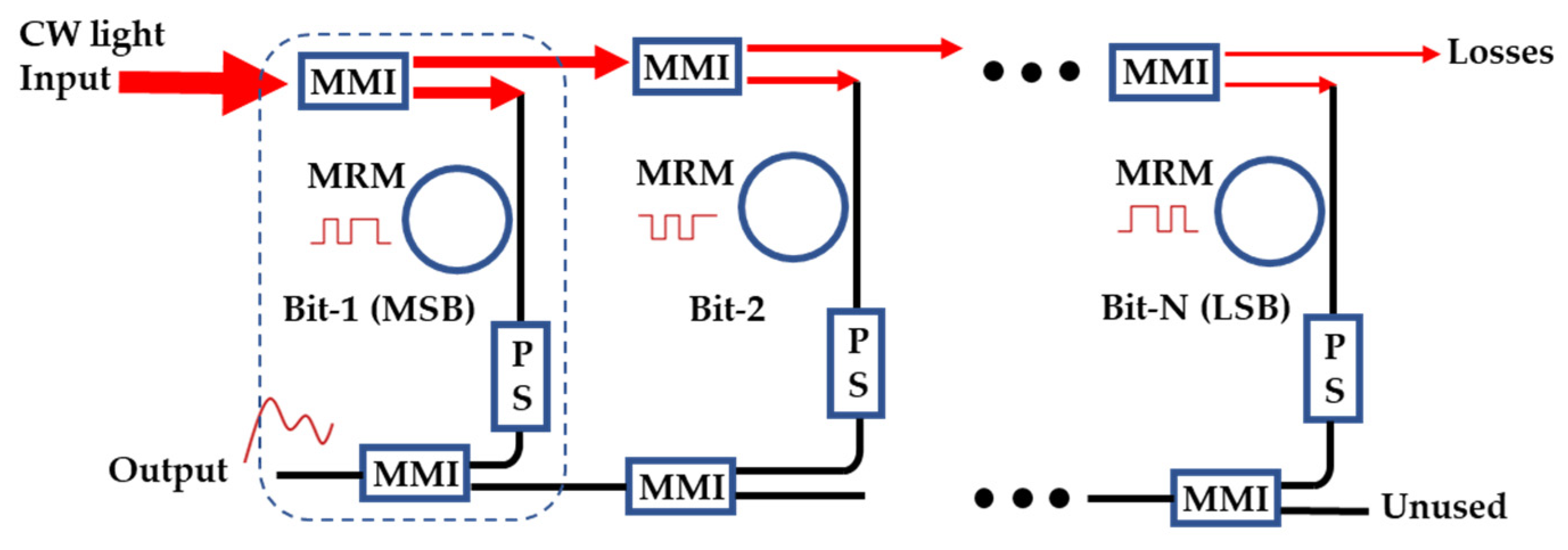
2. The Proposed Parallel PDAC Architecture
A schematic diagram of the proposed architecture is shown in
Figure 2. The system comprises ring resonator-based modulators, phase shifters (PS), and multimode interference couplers (MMIs). The MRMs process digital input signals by performing amplitude modulation on the continuous-wave (CW) carrier optical signal. This modulation is achieved by utilizing the change in the refractive index due to carrier depletion, allowing fast and efficient modulation while occupying a small footprint on the photonic integrated circuit (PIC). In the chip layout design, MRMs are directly sourced from the Advanced Micro Foundry (AMF) process design kit (PDK) library [
25]. Low-speed thermo-optic phase shifters are employed to ensure constructive interference for the coherent coupling of modulated optical signals. The MMIs function as 3-dB splitters for the input CW optical signal (weighting scheme) and subsequent combiners for the modulated coherent optical signals. The weighting scheme relies on each 3-dB MMI splitter allocating 50% of its input intensity to the connected MRM and phase shifter (PS) branch, with the remainder directed to the next splitter for lower-order bits. This way, the monotone carrier signal from a single CW light source is exponentially distributed among the modulator branches, starting from the most significant bit (MSB) on the left and successively towards the least significant bit (LSB) on the right. In this topology, the PDAC output is given by the interference happening at the summation of the branches. The dynamic range is the same as the dynamic range of an individual MRM (all MRMs are designed to be identical). Under the idealized assumption of MRM having infinite ER, the PDAC output is linear in field and quadratic in intensity [
18]. By reducing the MRM ER, the PDAC output intensity becomes more and more linear, but at the cost of reduced dynamic range.
To operate efficiently at a designated carrier frequency, it is imperative to synchronize all resonances of the ring modulator. However, the inherent sensitivity of ring resonators to fabrication imperfections, such as variations in waveguide width and thickness, and mismatches in the ring–bus gap, poses a challenge. These imperfections result in disparate resonance wavelengths among the ring modulators. To overcome this challenge, each MRM incorporates an electrical heater, facilitating the tuning of resonance frequencies to align with the desired carrier frequency.
One of the advantageous features of this PDAC topology is its modular design, allowing seamless accommodation of any desired number of parallel bits, with the pragmatic limit that the least significant bit remains distinguishable, assuming the photodiode in use is sufficiently sensitive. This scalability is achieved by the straightforward addition of an extra module (marked by a dotted box in
Figure 2: a branch consisting of two MMIs, an MRM, and a PS), requiring no change to the earlier branches. Thus, the maximum number of bits that can be accommodated is constrained by factors such as the signal-to-noise ratio or the bit error rate. Several sources contribute to the noise in this system, including resonance drift caused by temperature fluctuations, amplifier noise in the modulating RF signal, and the photonic shot noise originating from the photodiode. As the optical signal intensity decreases for subsequent bits, there comes a point where the signal power in the LSB branch becomes comparable to the noise level. This phenomenon imposes limitations on the scalability of the proposed PDAC architecture. Assuming that a commercial VCSEL is used as the CW light source that emits 10 dBm optical power at the operating temperature, 1 dB insertion loss can be considered for a standard edge coupling or photonic wire bonding to the PDAC chip. Assuming 0.1 dB insertion loss for an MMI, 0.5 dB loss for the MRM, and considering the operating point being located on the slope of the resonance dip (7 dB below the peak transmission off the resonance, asas discussed in the next section), roughly seven bits can be accommodated for an error-free DAC operation, with an average optical power of −20 dBm in the LSB if the system noise is below −23 dBm.
In its standard configuration, the PDAC output is an analog optical signal, suitable for pulse amplitude modulation (PAM). The individual microrings operate as intensity modulators with minimal phase modulation for constructive interference at the MMI summations. We use MRMs operating in the under-coupled regime to suffice these criteria, as illustrated by the phase response of the MRM (shown in
Figure 3a), which is measured using an optical vector analyzer. The PDAC output is a PAM-2
N signal where N is the number of parallel MRMs of the PDAC. In addition to PAM, the proposed PDAC architecture can also be used to generate coherent quadrature amplitude modulation (QAM). Two parallel PDACs are needed, one generating the I-component, and the other the Q-component of the QAM signal. In such a scheme, the PDAC architecture remains unchanged, but the microrings must operate as π-phase shifters with a constant steady-state amplitude. This can be achieved with MRM in an over-coupled regime, as seen in
Figure 3b. By operating the MRMs this way, the PDAC output is no longer of a PAM nature, but a coherent I- or Q-component of the 2
N-QAM signal.
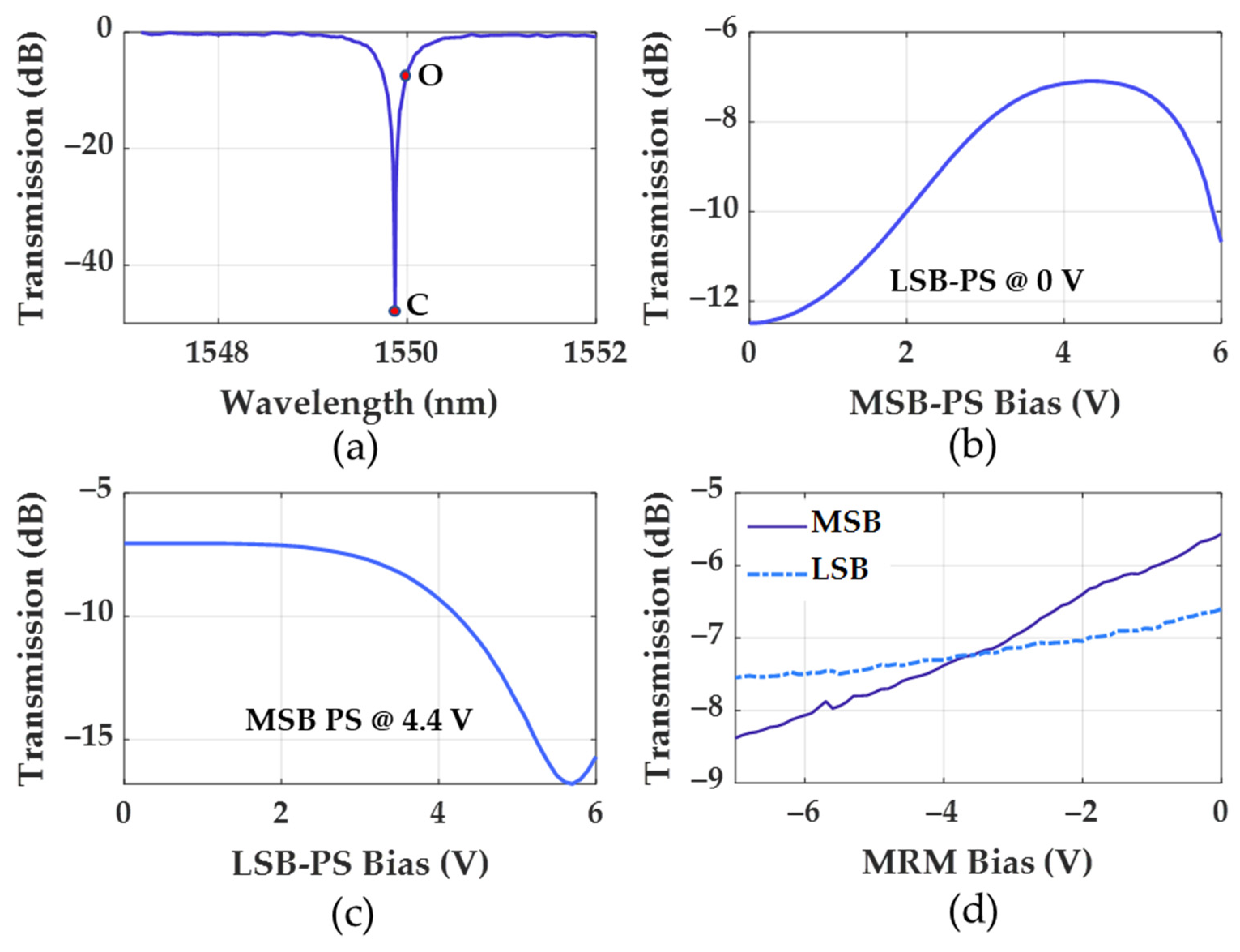
3. Alignment of the Resonances and the Dynamic Range
The MRMs are designed identically to have the same properties, but their resonances usually occur at different wavelengths due to fabrication imperfections. By tuning the ring heaters, i.e., applying a bias voltage as needed, all the MRM resonances can be aligned to the center wavelength (marked as “C” in
Figure 4a), and the PDAC extinction ratio becomes maximal, as shown in
Figure 4a. In all device operational temperatures, ring heaters draw a relatively low amount of power, ranging from 0 to 9 mW, to have all resonances aligned. This power could be avoided by post-fabrication trimming techniques [
26]. The center wavelength C is chosen such that the operating wavelength (marked as “O” in
Figure 4a) is located on either of the slopes of the resonance dip in the transmission spectrum. Before combining the modulated optical signals from each branch, their phases need to match for constructive coherent MMI coupling, leading to a correct representation of the analog output intensities. Thus, the phase shifters are tuned for constructive interference among the coupling signals, manifested by the maximum CW light transmission at the operating wavelength.
For correct phase shifter tuning, the ring modulators need to be aligned beforehand. Illustrated for a 2-bit PDAC,
Figure 4b shows the change in the CW signal transmission as the bias to the phase shifter connected to the MSB branch is varied between 0 V to 6 V, while the wavelength is set to the operating wavelength O. The maximum transmission is obtained at 4.4 V drawing 2.88 mA current by the PS thermal heater. Having this bias applied,
Figure 4c shows the PS voltage sweep of the LSB branch. The optimum transmission is obtained for a 0 V bias, while the previous PS is set to 4.4 V. The MRMs can be operated in two modes based on the plasma dispersion effect—carrier injection and carrier depletion. By biasing the modulator pn-junction in forward bias, carriers are injected to change the medium index, causing a resonance blue-shift. Since the pn-junction current increases exponentially with the applied forward bias voltage, the change in the medium index is accordingly high, resulting in a large resonance blue-shift. Biasing the deployed MRMs in the carrier injection mode, an approximately 0.8 nm/V wavelength shift is observed, corresponding to a relatively low V
π of 370 mV. In carrier injection mode, we experimentally achieved a maximum of 4 Gbps data rate with the 4-bit PDAC. However, because of the relatively long lifetime of the minority carriers, the carrier injection mode is not suitable for high-speed operation [
26,
27]. Therefore, in this work, we adopted the carrier depletion mode for PDAC operation.
Under the reverse bias condition, the carriers near the pn-junction are swept away by the applied electric field, widening the depletion region. This induces a resonance redshift through the plasma dispersion effect. The alteration of the effective refractive index is smaller than the carrier injection scenario although much faster. Our experimental study in the carrier depletion mode demonstrates a resonance wavelength shift of 14.3 pm/V. We chose 1550 nm as the operating wavelength. To determine the dynamic range of the MRM, a reverse bias voltage sweep is performed between 0 V and 7 V at 0.1 V increment steps. To find the intensity change contributed by an individual bit, the other ring modulator is kept aligned with the operating wavelength. In other words, the resonance associated with the other MRM is located at the center wavelength C.
Figure 4d shows the change in the optical intensity for the MSB and LSB. As the reverse bias is increased from 0 V to 7 V, the MSB contributes approximately 2.8 dB of extinction ratio, while the LSB contributes to a 1 dB difference.
5. Experimental Validation Results
The conversion rate of the 2-bit PDAC is determined using the above experimental setup, and a PAM-4 eye diagram is obtained on the digital communication analyzer (DCA). An on-chip back-to-back power transmission excluding the DUT demonstrates an approximate 10 dB of loss. Moreover, the transmission at the operating wavelength, located on the slope of the resonance dip, is lower than the peak transmission off the resonance dip. At the operating wavelength, while the ring modulators are biased at 3.5 V reverse bias, the steady state DUT output optical power is only −7.2 dBm. Therefore, the analog output signal is amplified to 1 dBm average power using an EDFA. A tunable optical bandpass filter with a 0.85 nm bandwidth is deployed afterward to filter out the amplified spontaneous emission (ASE) noise of the EDFA. The filtered analog signal is then converted to an analog electrical signal with a photodetector (PD) to be prepared for the DCA.
Figure 6a shows the eye diagrams of the 4 Gbps NRZ electrical signal from one of the data channels of the PPG with a resulting Q-factor of 10.4 dB (a). In
Figure 6b,c, the PDAC analog output exhibits a Q-factor of 7 dB and 6.5 dB when the MSB and the LSB are modulated, respectively.
Finally, in
Figure 6d, the PDAC analog output shows four distinct levels when both bits are modulated. The eye diagram experimentally validates the successful conversion of the parallel digital signal into an analog optical and later analog electrical signal, which is supported by the effective number of bits (ENOB) value of approximately 2.2 in our repeated measurements. In terms of linearity in the transfer characteristic, to quantify its deviation from an ideal DAC (a linear increase in the output level by 1 LSB for an increase in the input digital code by one), the differential non-linearity (DNL) of the DUT is found to be 0.4 LSB.
The experimental demonstration of the photonic digital-to-analog conversion at high speed beyond two bits could not be performed because of equipment limitations. By applying DC biases to the p–n junctions of the four MRMs, 16 intensity levels were obtained at the output of the 4-bit PDAC (
Figure 7). The applied DC forward bias signal shifts the resonances to shorter wavelengths by carrier injection, manifested by the increase in the PDAC signal.
Figure 7a illustrates a possible operating wavelength (dashed vertical line at 1551.15 nm) at which different 4-bit sequences produce corresponding intensity levels. In the linear scale,
Figure 7b shows the corresponding PDAC output power at the operating wavelength (1551.15 nm). The nonlinear relationship between the bit sequence and output power is explained by the unequal distribution of the input optical power to the MRM branches (an MRM branch receives 50% CW optical power compared to its preceding branch, and the output power is given by the interference of the signals in all branches). The random fluctuations in the spectrum (consequently, in the power levels) are caused by noise in the bias voltages and the MRM driver voltages, as well as room temperature fluctuations (causing resonance drifts), and contribute to a DNL of approximately 0.6 LSB (relatively larger than that of the 2-bit PDAC). In practice, the MRM requires tuning control to stabilize the output optical power.
6. Discussion
The chips were fabricated at the Advance Micro Foundry (AMF) in Singapore. In the layout design, we used the MRMs with a 22 GHz optical bandwidth from the foundry’s proprietary process design kits [
25] for a proof-of-the-concept demonstration. The chip was fabricated through a multi-project wafer (MPW) fabrication run, which is an experimental implementation of AMF’s MRMs using a set of doping concentrations that are different from those in the PDK design. Consequently, in addition to a low modulation speed, the MRM resonance shift under reverse bias obtained in the experiment turned out to be much lower than expected, resulting in small dynamic ranges and limiting the number of bit operations. Subsequent design optimization in the ring–bus gap, the optical path length of the MRM branches, doping concentrations, and the MRM thermal heaters have revealed promising prospects for enhancing the performance of the PDAC. For the standard doping concentration in the PDK design, MRMs with 10
radius and a 380 nm ring–bus gap, simulation results show a significant increase in modulation efficiency and speed. For this set of parameters, we simulated a 25 GBaud PAM-4 operation with a dynamic range of approximately 7 dB (compared to an approximately 3 dB value realized previously), which shows good agreement with the PDK specifications.
Moreover, in our first design prototype, different arms of the PDAC were not balanced, i.e., unequal optical path lengths among the MRM branches, which requires additional tuning of the phase shifters to ensure constructive interference among the modulated signals. However, this corrective measure incurred additional power consumption, contributing to the overall energy budget. To minimize the energy cost, it is recommended to design the PDAC with all branches having an equal optical path length for uniform propagation losses in every channel, leading to better output linearity and minimum tuning requirements from the phase shifters. This will also minimize the adverse effects that may be caused by the phase noise of the laser since the random fluctuation of the phase at the laser output will propagate coherently through the PDAC MRM branches and interfere constructively at the output. Another consideration for a robust PDAC architecture is the replacement of passive power splitters, such as the MMIs in this work, with tunable directional couplers [
28]. The optical signal in an MRM branch (a bit module) traverses two additional MMIs compared to that in its previous module, while the rest of the components in the module are exactly traversed once. Therefore, starting from the MSB, the optical signals in the subsequent modules encounter additional insertion loss of the MMIs, which is below 0.15 dB in the C band (1530–1565 nm). Additionally, depending on the operating wavelength, the slight imbalance of the power splitting ratio of the MMI, varying within ±0.1 dB in the C band, can compensate for the insertion loss (by transferring relatively more power into the upper output waveguide) or further exacerbate the distribution of the optical power in undesired splitting ratios to the subsequent modules. Given the dynamic range of the LSB being 1 dB in this work, the MMI insertion loss and imbalance would not jeopardize the bit resolution significantly. The deployment of the tunable directional coupler can mitigate the risk of degradation of the bit resolution resulting from the optical component losses and imbalances.

 ,
, 