Article

Thin and Large Depth-Of-Field Compound-Eye Imaging for Close-Up Photography

1
Beijing Engineering Research Center of Mixed Reality and Advanced Display, School of Optics and Photonics, Beijing Institute of Technology, Beijing 100081, China
2
Beijing Ned+AR Ltd., Beijing 100081, China
3
Key Laboratory for Physical Electronics and Devices of the Ministry of Education and Shaanxi Key Laboratory of Information Photonic Technique, Xi’an Jiaotong University, Xi’an 710049, China
*
Author to whom correspondence should be addressed.
Photonics 2024, 11(2), 107; https://doi.org/10.3390/photonics11020107
Submission received: 22 December 2023 / Revised: 16 January 2024 / Accepted: 17 January 2024 / Published: 25 January 2024

Abstract

:
Large depth of field (DOF) and stereo photography are challenging yet rewarding areas of research in close-up photography. In this study, a compound-eye imaging system based on a discrete microlens array (MLA) was implemented for close-range thin imaging. A compact imaging system with a total length of 3.5 mm and a DOF of 7 mm was realized using two planar aspherical MLAs in a hexagonal arrangement. A new three-layer structure and discrete arrangement of sublenses were proposed to suppress stray light and enable the spatial refocusing method, which restores image information at different object depths. The system is successfully fabricated, and the system performance is carefully investigated. Our system offers a large depth of field, high resolution, and portability, making it ideal for close-up photography applications requiring a short conjugate distance and small device volume, while also addressing the issue of crosstalk between adjacent channels.

1. Introduction

In close-up photography, a traditional optical lens requires a complex optical structure to correct aberration encountered with a large field of view (FOV), aperture, and DOF. Furthermore, the total thickness of the system is difficult to compress. If the method of capturing the whole image by a single system is divided into multiple sub-systems to capture part of the image, the FOV, and aperture of a single system can be reduced. Therefore, a relatively simple and thin system can be used to achieve clear imaging.
The insect eye, or compound eye, is a naturally formed complex optical system. In contrast to the single-aperture eyes of vertebrates, the compound eyes of insects have a very large FOV, low aberration and distortion, high temporal resolution, and an almost infinite depth of field (DOF) [1,2]. Compound-eye imaging systems typically consist of multiple microlenses for imaging and a single photodetector for sensing [3,4]. Several methods have been employed to manufacture high-quality microlens arrays (MLAs), including laser-induced self-writing [5,6,7], two-photon polymerization [8], and projection lithography [9]. In addition, polymer swelling [10,11] and thermal reflow [12] have been used to fabricate MLAs with tunable surface profiles.
Each element of an MLA captures information regarding the particular direction and angle of the incident light rays in the overall scene. Individual images can then be superimposed to obtain continuous general information regarding the imaged object. This has led to the widespread use of MLAs in applications such as light-field acquisition and imaging [13,14,15,16], three-dimensional integrated imaging [17,18,19], and other micro-optic applications [20,21,22,23]. For example, phase-diffraction MLAs with large relative apertures, small relative thicknesses, and compact compound-eye imaging modules can be used for fingerprint imaging [24]. Popular applications, such as post-shot refocusing and changing viewpoints, have been demonstrated using light-field cameras [13], whereas multilevel diffractive lenses (MDLs) can be used for long-distance imaging with a large DOF [25]. Even in close-range photography, the depth information of the object is also very important. A large DOF helps to clearly identify the depth of detailed features, which is very useful for shooting tiny organisms with close-up shots and diagnosing diseases with endoscopes [26,27]. In the field of close-ups using MLAs, the work of Berlich et al., only analyzed the image quality at fixed object distances [28]. In this work, we propose a lightweight and compact close-up system through optical design and a refocusing algorithm for large-DOF imaging. In fact, applications of that technique have been limited to short-range stereo imaging. To address the issue of stray light, previous studies have used a grid between the MLA and the CMOS detector [4]. In order to shorten the length of the system, three layers of apertures are used to eliminate stray light, and the thickness of the diaphragm is approximately 10 μm.
To achieve these objectives, Dual MLAs with micron precision have been developed. Section 2 describes the principles of multifocal integral imaging using MLAs, defines constraint relations between the sizes and refocusing depths of multifocal imaging, and explains our spatial algorithm for improving the refocus ability of objects at different depths. Section 3 presents the design and analysis of our aspherical sublens, which features a three-layer structure aimed at eliminating crosstalk. The large depth of field of the system is realized by controlling the aperture of the sublens, shortening the back focal length (BFL) and setting multiple object distances during the optical design. Using the refocusing method, a picture taken by this system can be focused in any plane within the depth of field. Additionally, we performed an offsetting matrix analysis of our hexagonally arranged MLA. In this study, we also derived the pixel utilization and introduced a method for estimating shooting depth. Section 4 details the experimental setup and procedures we conducted to validate the effectiveness of our proposed method.

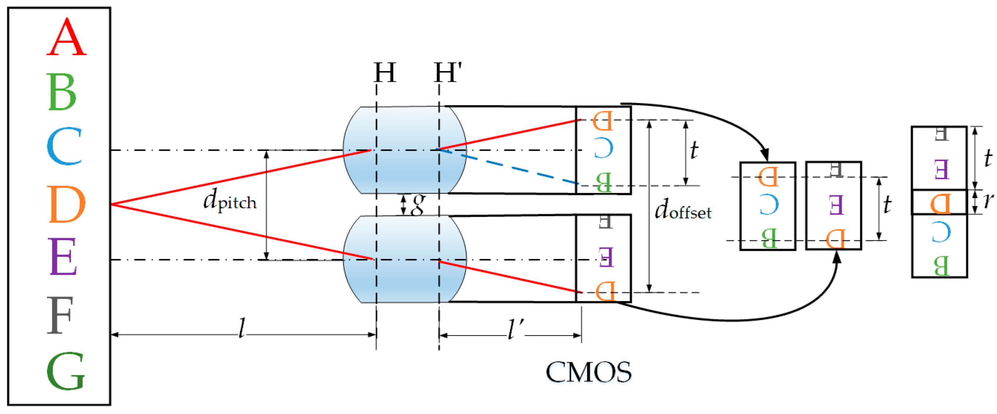
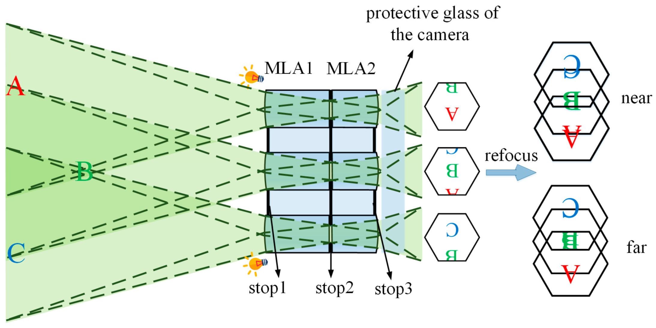
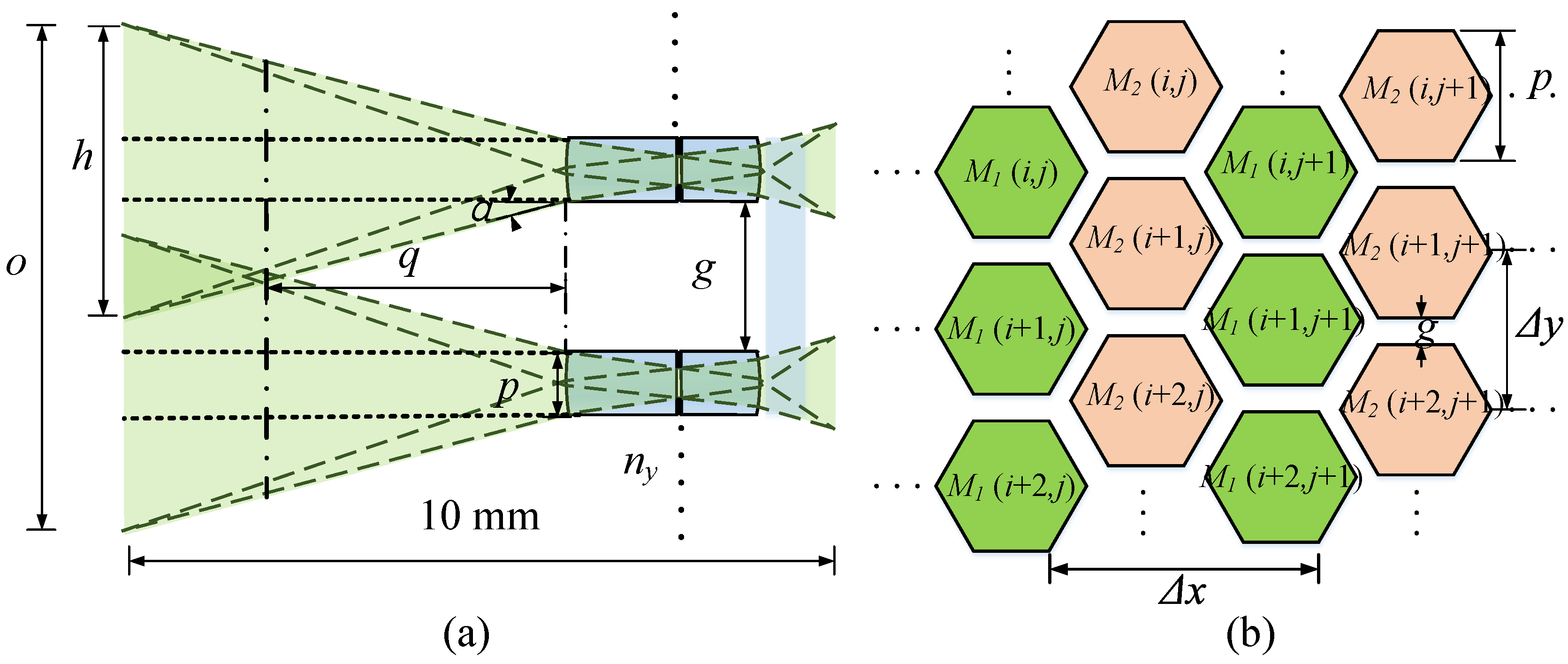
2. Principles of Micro Compound-Eye Optical Design

A compound-eye imaging module is proposed in our design for capturing three-dimensional objects. It consists of two discrete MLAs, a three-layer structure for eliminating stray light, and an image sensor, as shown in Figure 1. Compact, lightweight hardware was made by first planarizing the MLAs. Each sublens is a basic imaging system that forms an elemental image based on Gaussian optics. Stray-light-eliminating structures were added to the front, rear, and inner surfaces of each microlens to prevent crosstalk between adjacent channels. The introduction of lighting can help increase brightness in dark environments.
Our system is capable of imaging objects with a large DOF and can yield a set of elemental images that can be integrated into a compound image owing to the small aperture of each microlens. Each sublens observes a portion of the object from its unique position and perspective. Therefore, every elemental image contains unique sampling information that can be combined to reconstruct a final image [24]. The magnification ratio of our imaging device was set to less than 1, and elemental images were offset and superimposed. Similar to a light-field camera, our system allows for the refocusing of objects at different depths within the DOF after a single snapshot.
Figure 2 illustrates the geometric relationships between each subchannel in our system. The chief rays from a single object point passing through two subchannels are shown as solid red lines, while the blue dotted line represents the auxiliary line parallel to the outgoing light of an adjacent subchannel. H and H′ represent the principal planes of the object and image of the microlens, respectively; l indicates the object distance; l′ denotes the image distance; and dpitch refers to the pitch between adjacent microlens centers. Furthermore, t represents the offset of the local position of a point with the same information as in the adjacent elemental image. The uniform refractive index of the microlens ensures that the principal plane and the nodal plane are the same. According to the principle of similar triangles, t is calculated using Equation (2) as follows:
β = l l ,
t = β d pitch ,
Equation (2) shows that t is equal to the product of the distance between subchannels and the system magnification, and doffset is the distance of the imaging point after the object point passes through the adjacent sublens. That offset is calculated using Equation (3):
doffset = dpitch + t,
where g represents the gap between adjacent lenses and r represents the amount of overlap between neighboring elemental images after refocusing, which is calculated using Equation (4) as follows:
r = dpitchgt.
A 3-D scene can be computationally reconstructed by simulating the optical back-projection of elemental images [29,30,31]. Reconstruction involves the inverse mapping of elemental images to object spaces such that individual images overlap with all other back-projected images, enabling the light field to be reconstructed in arbitrary planes within a 3-D object volume.
Using the geometric relation deduced above, elemental images were offset and superimposed. We selected the elemental image in the upper-left corner as the benchmark for offsetting other elemental images. The offset value of each adjacent elemental image in the Y direction is doffset., which was calculated using Equation (3) under paraxial conditions. The error in calculation results increased with the increase in FOV. In practical applications, the function of manually adjusting the doffset is added to the software to reconstruct the image at different depths. Elemental images at other locations were offset according to the geometric relation described in Section 3 [32]. To maximize accuracy, the pixel number of the element image being offset was not rounded until the last stage of the calculation. In order to ensure the uniformity of the brightness of the pixel overlay region when elemental images were offset and superimposed, the contributions were averaged from multiple elemental images.

3. System Implementation
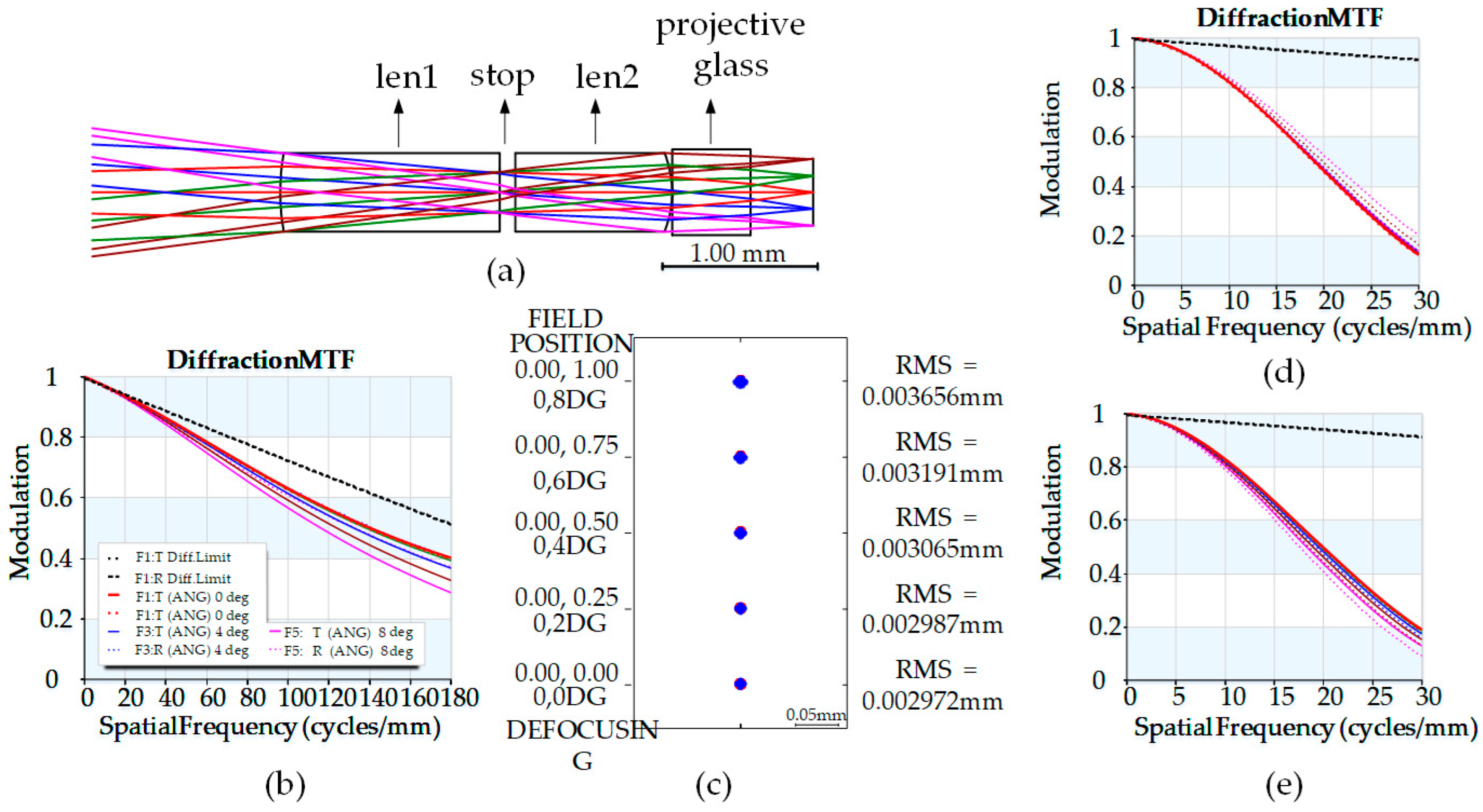
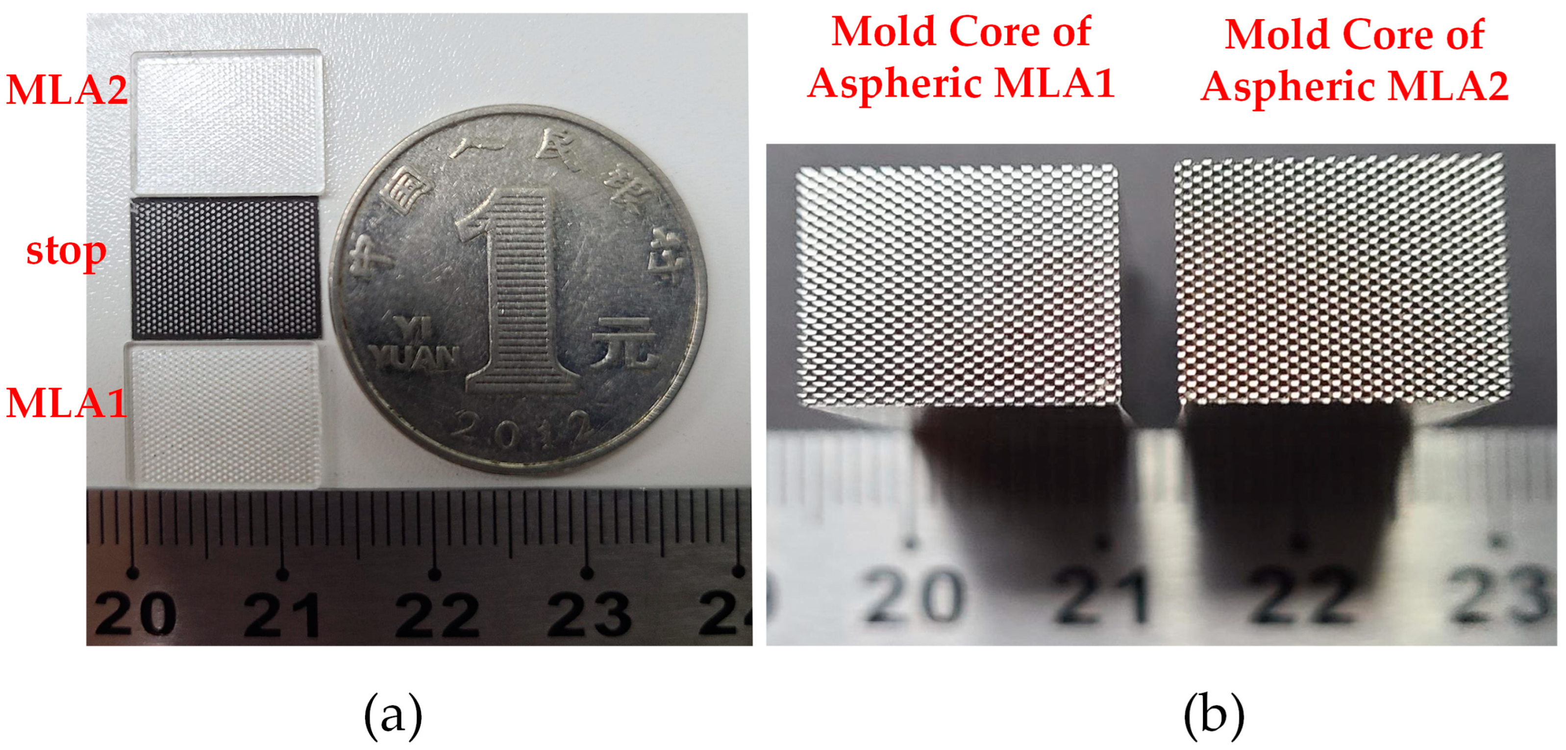
3.1. Optical Design

Three parameters that affect DOF include the focal length, object distance, and aperture size. MLA having a short focal length and small aperture can achieve a large imaging DOF at short distances. Before analyzing and manufacturing a complete MLA, an individual subchannel was analyzed and designed.
The subsystem diameter must be kept small to control the amount of light passing through the system and improve image quality. At the same time, in order to reduce the sag of the sublens, the diameter of the sublens is controlled within 0.5 mm. The diameter of our aperture stop was set to 0.12 mm, and the conjugate distance of our system was controlled to within 10 mm to enable close-up photography in a limited space.
DOF for a constant conjugate distance can be improved by minimizing the back focal length (BFL) distance and increasing the object distance. Considering the 0.5 mm thickness of the front protective glass of the complementary metal oxide semiconductor (CMOS) and the 0.4 mm gap between the protective glass and photosensitive region, it was not possible to make the BFL less than 0.9 mm in our setup.
A two-lens optical system with an inner aperture stop was used to control the diameter of the light beam. The surfaces of the two lenses in contact with the aperture stop were made flat to avoid the influence of mechanical stress and facilitate assembly. However, the two surfaces of the lens away from the aperture were made aspheric to expand the FOV and improve image quality. We take all of these factors into account in the optical design with CODE V. The aspheric surface usually can be expressed as:
z = c r 2 1 + 1 ( 1 + k ) c 2 r 2 + i = 2 n a 2 i r 2 i
z is the sag of the surface parallel to the z-axis. c is the curvature at the pole of the surface. k is the conic constant. r is the radial distance. a2i is the order deformation coefficient, respectively. Although both lenses were more than 1 mm thick, the overall system thickness was less than 3 mm. The object distance of the system is set in the range of 4~14 mm, and the optimization results for the parameters listed in Table 1 are presented in Figure 3.
Our system exhibited high image quality at the optimal object distance. Specifically, the Modulation Transfer Function (MTF) was greater than 0.2 at 200 line pairs per millimeter (LP/mm), astigmatism of marginal FOV was less than 0.05 mm, distortion was less than 2%, and the RMS spot pattern was less than 0.004 mm. Because the magnification of the system varies with object distance. In the distance range of 4 mm to 14 mm, the magnification of the system varies from 0.1 to 0.3. The MTF at 25 LP/mm was greater than 0.2 when the object was 4 to 14 mm away. According to the imaging capability of the system, an object distance corresponding to MTF greater than 0.2 at 25 LP/mm is defined as the range of DOF. This resulted in a DOF of approximately 10 mm. To predict the actual performance and yield of the product, based on the known machining capabilities of the supplier, a tolerance analysis was carried out. The sensitive items for each tolerance type are shown in Table 2. 2000 Monte Carlo simulation trials were carried out, and Figure 4 shows the cumulative probability for different MTF values under the conditions in Table 2. The MTF for all fields has an 88% chance of being above 0.15.
The size and arrangement of the MLA’s sublenses are key factors in determining the system’s imaging capabilities. When no gaps exist between microlenses, the information collected is redundant, resulting in crosstalk. However, when the gap between sub-images is too large, it is not conducive to the reconstruction of the complete image.
Thus, to avoid an imaging gap, it is important to find the maximum lens gap for which full object information can be captured within the DOF. As shown in Figure 5a, it is difficult to capture complete information when the object is close to the lens (<1.1 mm). Half of the FOV ω of the subchannel is 8°, and the maximum acceptable lens gap g at the closest distance (4 mm) within the DOF can be calculated using:
g 2 q   tan ω ,
where q denotes the nearest distance in the DOF. In this study, the maximum gap g of the MLA was 1.1 mm, and the overall size of the MLA was 13 mm × 10 mm (matching the one-inch CMOS). In the y-z view, the number of sublenses is ny, the vertical height of the subchannels is p, and the imaging range of the subchannels is h at the designated object distance shown in Figure 4a. The overall imaging range o of the MLA can be calculated as follows:
o = ( n y 1 ) ( p + g ) + h .
The imaging range of the x − z view can be similarly obtained, and the image size of the entire system can be calculated as 14.875 mm × 12.165 mm. Figure 5b shows the hexagonal arrangement of sublens. The sublens position in the hexagonal design of an MLA can be decomposed into two rectangular structures corresponding to matrices M1 and M2. The sublens spacing in the y- and x-directions is given by Δy = p + g and Δ x = 3 ( p + g ) , respectively. As shown in Figure 5b, M1(i, j) and M2(i, j) are the coordinates of the sublens corresponding to matrices M1 and M2, respectively. Sublens positions can be obtained using matrices M1 and M2 as follows:
M 1 ( i , j ) = X D E ( i , j ) Y D E ( i , j ) = ( i i c e n t r a l ) Δ x ( j j c e n t r a l ) Δ y = ( i i c e n t r a l ) 3 ( p + g ) ( j j c e n t r a l ) ( p + g )
M 2 ( i , j ) = M 1 ( i , j ) + 3 ( p + g ) 2 ( p + g ) 2 = ( i i c e n t r a l ) 3 ( p + g ) + 3 ( p + g ) 2 ( j j c e n t r a l ) ( p + g ) + ( p + g ) 2
where XDE(i, j) and YDE(i, j) are the decentering amounts of the sublenses with reference to the central sublens [31]. The specifications of this system are given in Table 3.

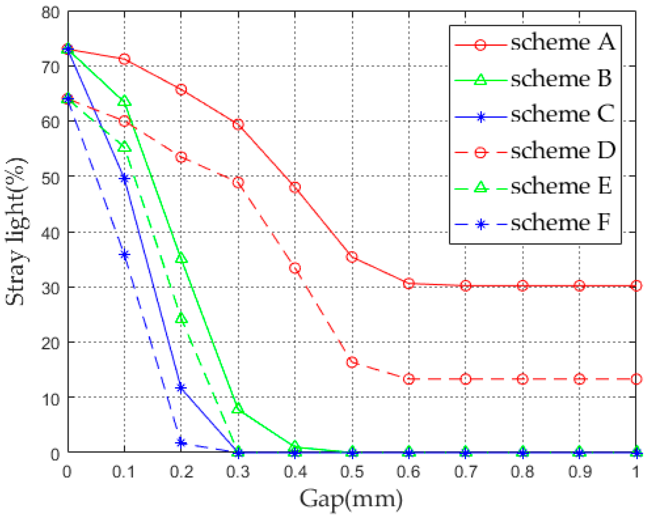
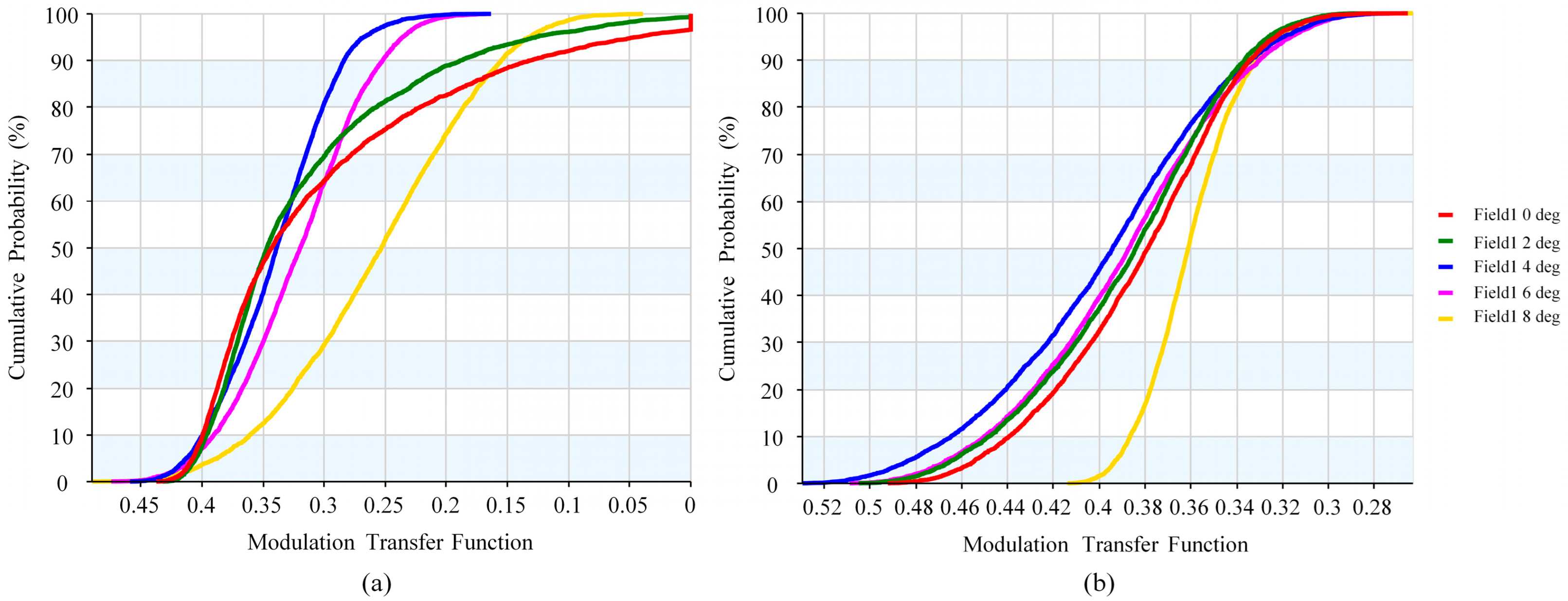
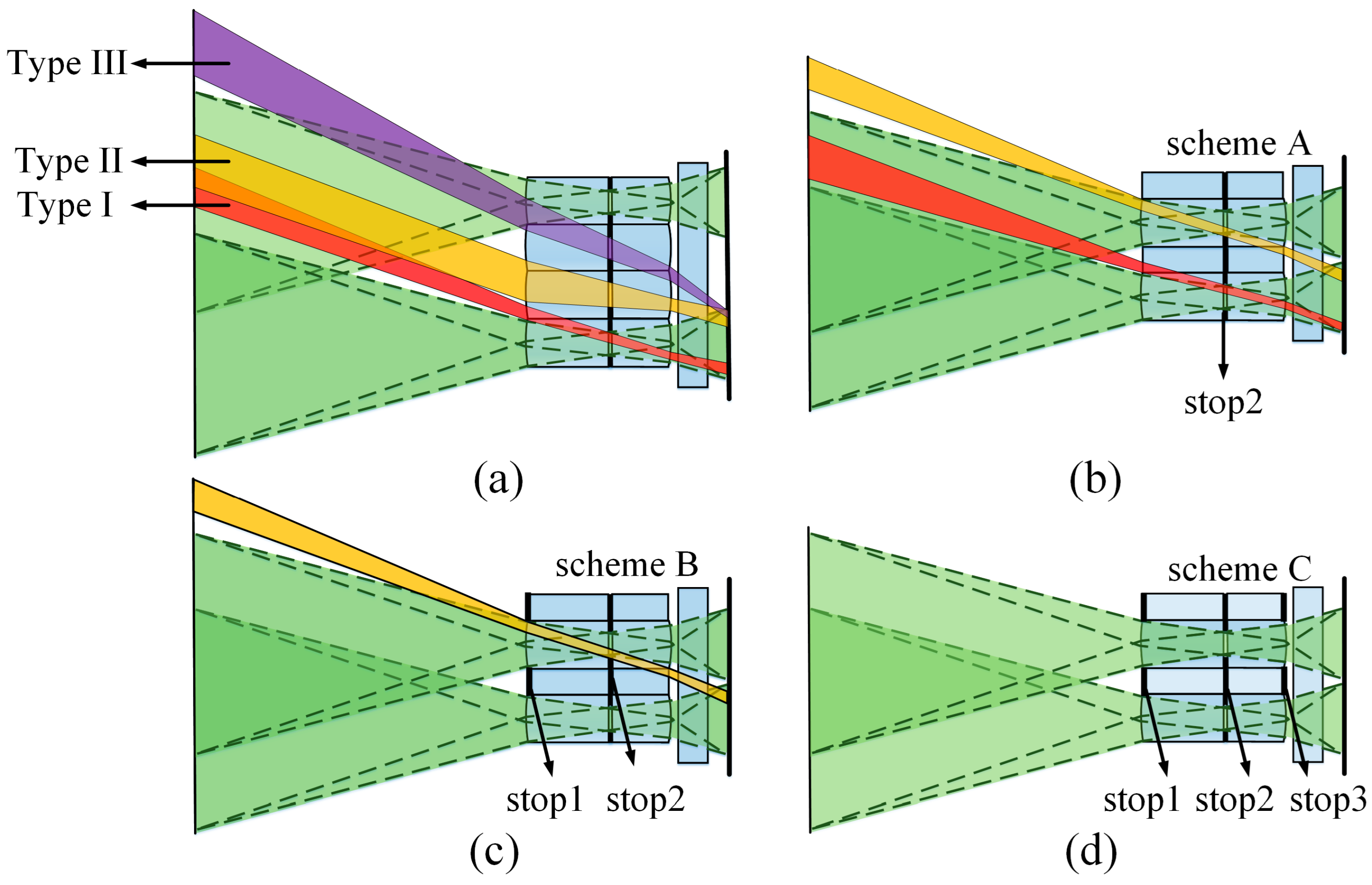
3.2. Stray Light Analysis and Elimination

Ideal imaging for an MLA system occurs when each subchannel is not influenced by other channels (i.e., no crosstalk). Specifically, a single spot in the image plane is ideally formed by a light ray passing through the front and rear surfaces of a single sublens. However, in practical systems, crosstalk between channels can occur. In Figure 6a, the green light beam represents the ideal light path (i.e., normal light) when microlenses are closely connected. However, in practical systems, three types of stray light need to be considered. The red beam represents stray light generated through the same aperture as the principal beam, which is called “stray light type I”. The yellow beam represents stray light passed through an adjacent aperture, which is called “stray light type II”. The purple beam, “stray light type III”, is produced by the interphase aperture.
To address the issue of stray light, previous studies have used a grid between the MLA and the CMOS detector [4]. However, this approach is not practical for our system due to the 0.5 to 0.7 mm protective glass layer and 0.4 mm air space between the glass and photosensitive area of our detector, which results in a short (~1 mm) BFL system. Therefore, a new method to eliminate stray light in our system needed to be developed.
Figure 6b shows that when the microlenses are arranged discretely with a gap greater than a certain value, type III stray light can be eliminated with only stop2. This method is referred to as Scheme A. Figure 6c shows that adding a stop1 at the lens gap on the front surface of the lens can eliminate type I stray light. This is referred to as Scheme B. Figure 6d shows that a two-layer diaphragm can be added at the lens gap on the front and rear surfaces of the lens, respectively, to eliminate type II stray light. This method is referred to as Scheme C. The two aperture arrays block light only at the gap of the sublens. The size and arrangement of the two aperture arrays are exactly the same, which reduces the difficulty of processing and assembly. While reducing the aperture stop diameter can also be used to suppress stray light, such methods reduce lighting efficiency. Therefore, we also tested Schemes D, E, and F, where the aperture stop radius used in Schemes A, B, and C was reduced from 0.12 to 0.06 mm, leaving all other parameters unchanged.
To simulate stray light, we devised an optical system using LightTools. Because most objects reflect diffuse light, the divergence angle of the light source was set to 180° to capture all the stray light and ensure the effectiveness of our stray light analysis. The size of the entire object (15 mm × 12 mm) was placed at the maximum imaging range of the system, and the light source was made to shine uniformly. By setting a receiver on the image surface of a subchannel, both stray and effective light were captured. First, when only a single subchannel is opened, the energy received by the receiver has its optimal value. When all channels are opened, the energy received by the receiver is the total value. The ideal value divided by the total value gives the proportion of direct light vs. direct-plus-stray light. Stray energy was obtained by subtracting the ideal value from the total value. The proportion of stray light for our six schemes for different gaps between adjacent lenses is shown in Figure 7.
As shown in Figure 7, stray light can be effectively suppressed in a few different ways: by enlarging the lens gap, by increasing the number of aperture layers, and by reducing the aperture stop. For schemes A and D, when the lens gap is greater than 0.6 mm, increasing the lens gap no longer plays a role in suppressing stray light because stray light type I cannot be completely eliminated using stop2. In schemes B and C, stray light can be completely eliminated when the lens gap reaches a certain value. Shrinking the aperture size further reduces stray light. In order to improve light efficiency, the aperture of the diaphragm needs to be relatively large, and in order to capture the complete object in a large depth of field, the gap of the lens needs to be as small as possible. Under this premise, scheme C (gap = 0.3 mm) is more appropriate.

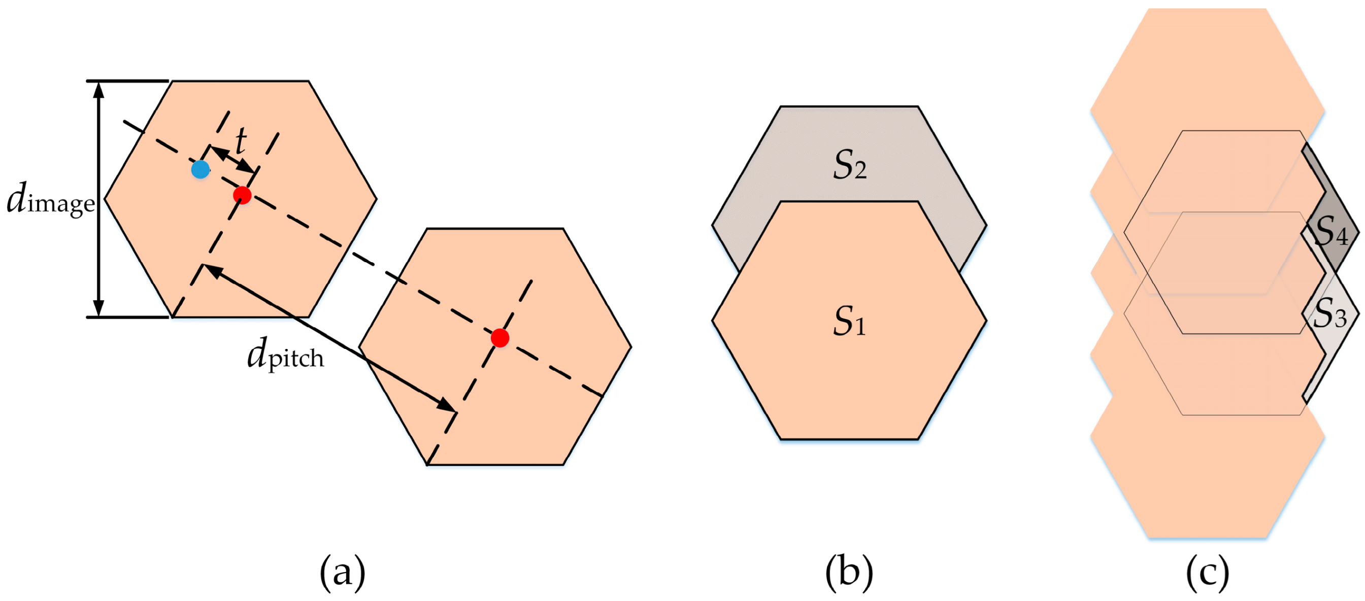
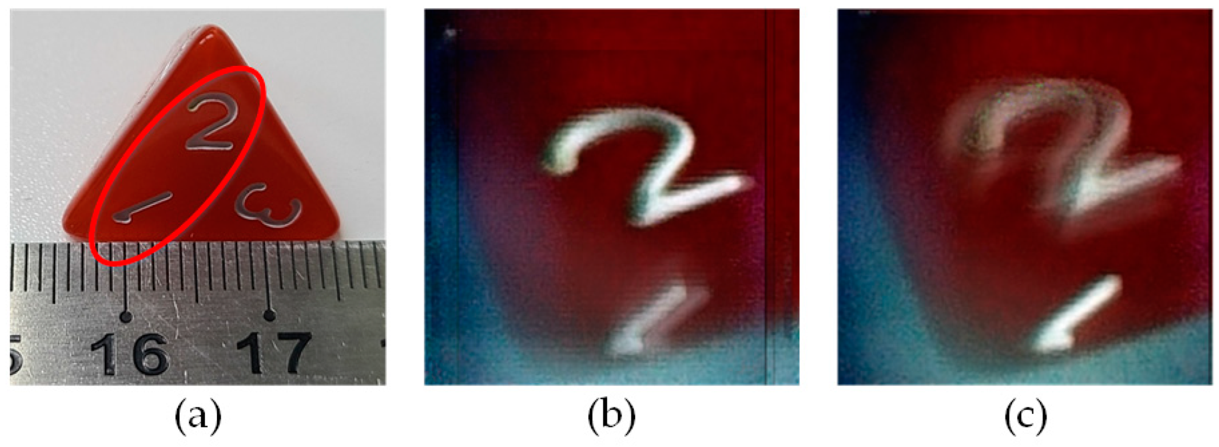
3.3. Pixel Utilization
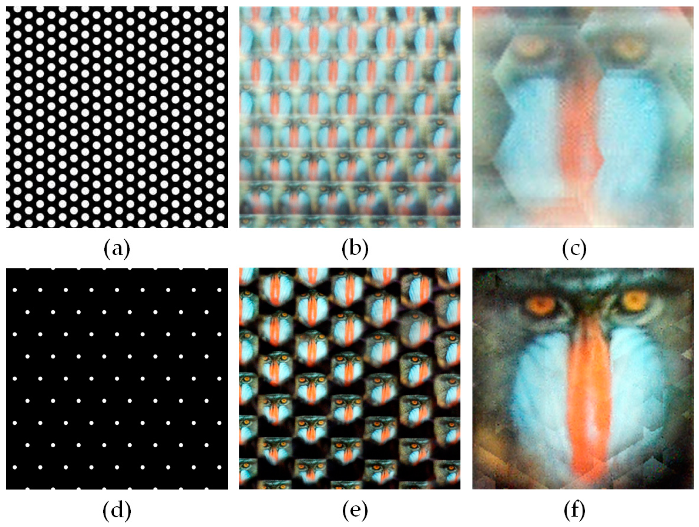
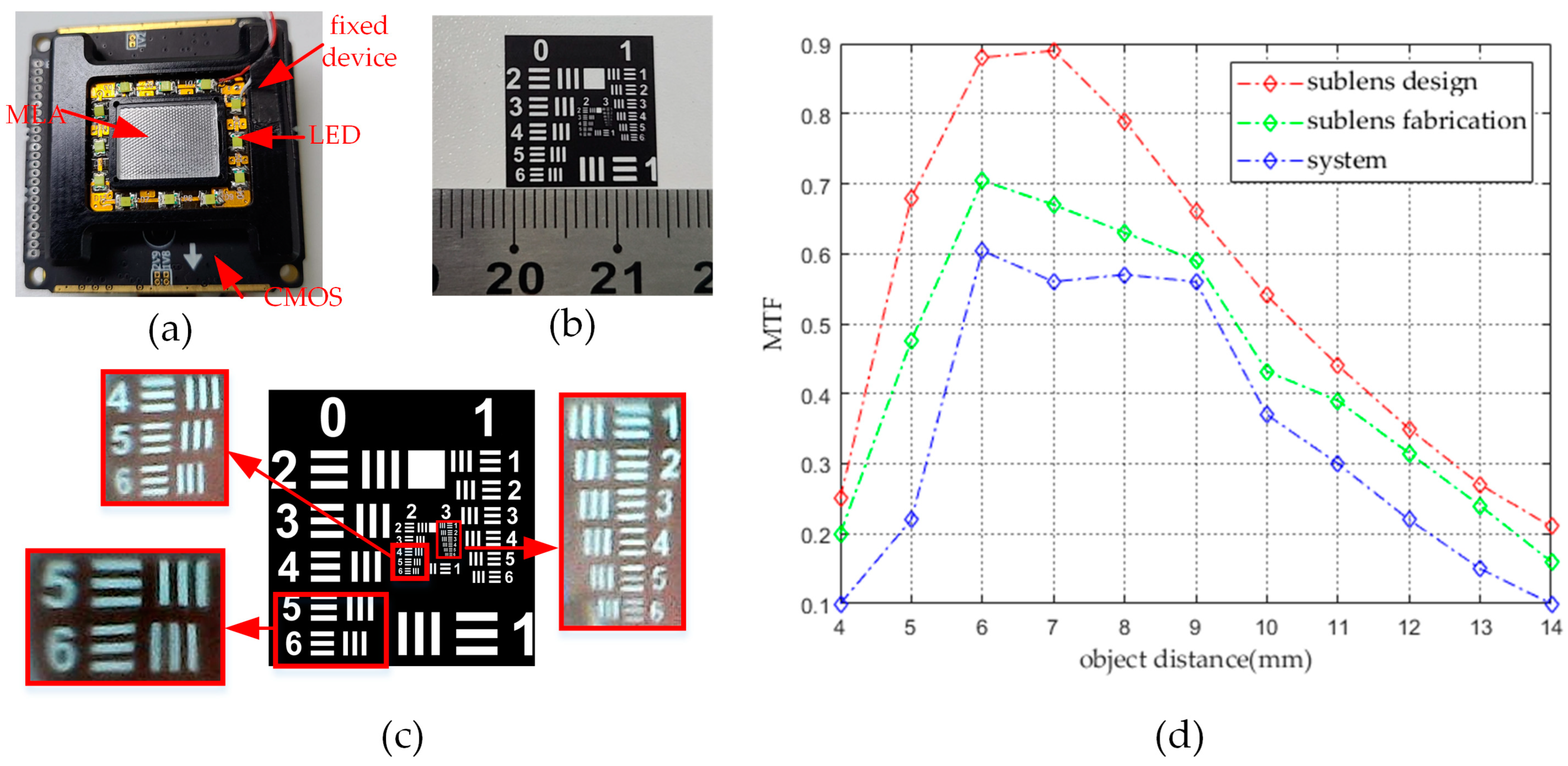
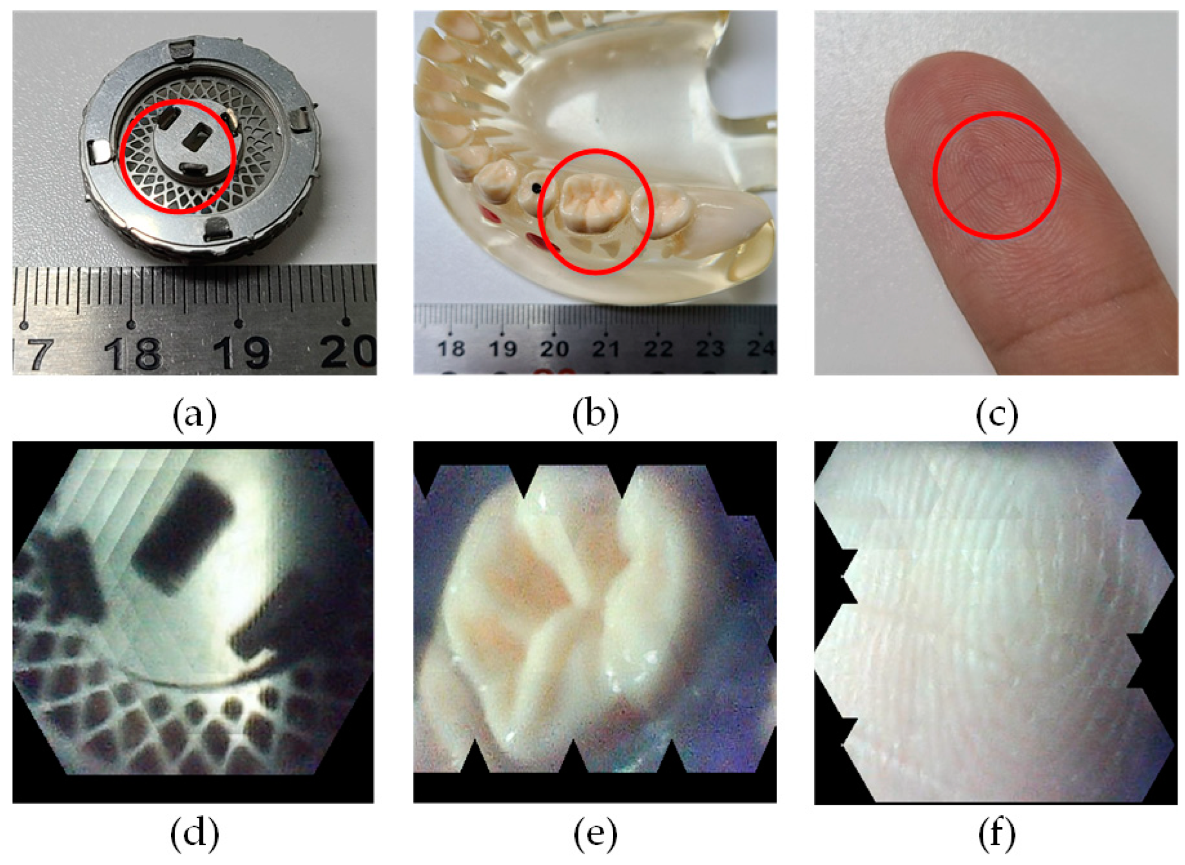
The image captured by this system contains duplicate sets of object information needed for refocusing, as previously shown in Figure 1. Therefore, the refocused image resolution is lower than the resolution of CMOS. Pixel utilization η is defined as the ratio of the refocused image resolution to the original image resolution. The geometric relationship between the two-dimensional images of the CMOS is shown in Figure 8a. The definitions of t and dpitch are the same as those used in Figure 2, and dimage represents the height of the elemental image in the vertical direction. The red dot represents the center of the subimage, and the distance between the blue dot and the red dot in the direction of the dashed line is t.
First, adjacent elemental images were refocused along the vertical direction, as shown in Figure 8b. The effective pixel contributed by the first elemental image is the entire hexagonal part S1. The effective pixel contributed by the second elemental image is the shadow part S2; and ny is the number of elemental images of each column. Therefore, the remaining effective pixel Scol after refocusing the elemental images of a single column is:
S col = S 1 + ( n y 1 ) S 2
The two adjacent columns of the images are refocused in the horizontal direction, as shown in Figure 8c. The shaded part is S3, and the area of the black solid part is S4. Therefore, the effective pixel increase achieved by refocusing the images in two adjacent columns along the x-direction is:
S r o w = S 3 + ( n x 1 ) S 4
where nx is the number of elemental images in each row. Therefore, pixel utilization is the effective pixel S of all elemental images after refocusing, divided by the original pixel S′ of the whole image:
η = S S = S col + ( n x 1 ) S row 3 2 d pitch 2 n x n y     = 3 2 d image 2 + ( n y 1 ) 1 2 3 ( 4 d image t ) t + ( n x 1 ) ( 3 t 2 + ( n y 1 ) 3 2 t 2 ) 3 2 d pitch 2 n x n y
When nx and ny are large enough, η can be approximated by:
η l l 2 .
It can be seen from Equation (13) that when the number of sublenses is large, pixel utilization approaches the square of system magnification. We also incorporated various parameters such as dimage, nx, and ny into Equation (12) according to specific scenes in order to predict the pixel utilization of the adopted structure.

4. Results

To reduce cost and verify the proportion of stray light for various lens gaps, MLA sublenses were closely connected for processing. Aperture stops were set to replicate the different gaps of the sublens. Experimental aspheric MLA1 and MLA2 elements and aperture arrays are shown in Figure 9a. MLA1 and MLA2 are MLA composed of lens1 and lens2 in Figure 3, respectively. The design parameters of the sublens are shown in Table 1. Both polycarbonate MLAs designed in this study were manufactured using high-precision injection molding. The mold cores of aspheric MLA1 and MLA2 are shown in Figure 9b. The fabrication precision of the MLA mold core surface was 0.3 μm, which is sufficient for imaging. The aperture arrays are fabricated using photolithography.
The rear surface of the optical system was close to the protective glass of the CMOS, and the ideal object distance was 6.65 mm. The entire system is shown in Figure 10a. Twelve LED beads with adjustable brightness were added to the grooves of the fixture to compensate for the lack of illumination under dark conditions. Through the structural design, the LED is embedded into the groove in order to avoid the light shining directly on MLA. The LED emits white light to avoid color bias of the illuminated object. The lamp beads can be regarded as Lambertian light sources, which are periodically arranged, and the object is uniformly illuminated. To verify the actual imaging effect, the 1951 United States Air Force (USAF) resolution test chart (Edmund, Positive 1951 USAF Hi-Resolution Target) was used as the imaging target, as shown in Figure 10b. The imaging effect for different target sizes is shown in Figure 10c. Owing to the small size of the CMOS, it was not possible to obtain a full-resolution board in one shot. Red arrows indicate the correspondence between the original and reconstructed images. According to the imaging capability of the system, an object distance corresponding to MTF greater than 0.2 at 25 LP/mm is defined as the range of DOF. The MTF of the sublens and the entire system at 25 LP/mm was tested and shown together with the design values in Figure 10d. MTF is obtained by photographing a black-to-white hypotenuse at different object distances using the SFR method. After refocusing, the MTF is still greater than 25 LP/mm when the object distance is from 5 mm to 12 mm. The depth of field is thus confirmed at 7 mm. The machining error of the sublens surface such as the PV value and roughness will affect the imaging quality of the subsystem. Assembly errors such as decentration and tilt can cause alignment errors between the two-layer lens array and the diaphragm. It will lead to the reduction in MTF and the generation of stray light. The offset and overlap of the sub-images will exacerbate the problems introduced before, resulting in the refocused image becoming more blurred.
An array of 0.12 mm apertures corresponding to the sublenses (gap = 0 mm) is called Aperture I, as shown in Figure 11a. An array of 0.06 mm apertures arranged in a discrete manner (gap = 0.317 mm) is called Aperture II, as shown in Figure 11d. Apertures I and II were used in the optical system to standard test image “Mandrill” (5 mm × 5 mm) displayed on a mobile phone. Local images of the CMOS are shown in Figure 10e and Figure 11b. Elemental images were refocused, and the results are shown in Figure 11c,f. Our experimental results agreed with our theoretical analysis. Namely, the discrete arrangement of the aperture (which matched that of the lens) and its reduced aperture effectively suppressed most stray light. It was also noted that when a large amount of stray light was present, color distortion of the image was observed.
In addition, we conducted experiments to demonstrate the prototype’s ability to refocus at different depths when photographing three-dimensional objects. As shown in Figure 12a, the compound-eye system was positioned above a triangular dice and take pictures of the contents in the red circle. In this configuration, number 2 is closer to the system than number 1. The results of focusing on numbers 2 and 1, respectively, are presented in Figure 12b,c. When the system is focused on number 2, it appears clear while number 1 appears blurry. When the system is focused on number 1, the opposite is true. These results demonstrate that the system can effectively refocus at different depths, enabling it to capture clear images of objects with varying distances from the system. Therefore, in order to obtain all clear objects in the DOF, several refocusing processes are required.
The imaging capability of the system for near-range 3-D objects was verified, as shown in Figure 13a–f. Figure 13d–f depict the results of refocusing different objects in the red circle using our system while controlling the object distance within a range of 1 cm. As the surfaces of fingers and teeth can be considered diffuse reflectors, the intensity of their reflected light is weak. Therefore, a white LED light source was necessary for illumination.
Finally, to avoid refocusing after every shot, a program was written that automatically refocused elemental images according to their input offset value. The system was connected to an Intel i7-9700 CPU. Real-time imaging was realized when the program was run at a refresh rate of up to 30 Hz. The RAM memory is 16 GB and the graphics card is RTX2060 of Nvidia Corporation. This enabled users to view refocused images directly and change offset values in real time to adjust image definition and focusing depth.

5. Conclusions

A thin compound-eye imaging system with a large depth of field based on discrete aspherical MLA has been proposed. We have derived the relationships between the optical and structural parameters and developed a stray-light-free model using three layers of apertures and a discrete sublens arrangement. Additionally, the pixel utilization and depth-of-field prediction of the system have been analyzed. Our experiments using a prototype system have verified its ability to zoom when imaging 3D objects at close range and produce clear images with a large depth of field. In the future, we plan to use a curved MLA to achieve a wider field of view and address residual issues, such as brightness uniformity with specular reflection and the loss of resolution due to elemental image overlap.

Author Contributions

Conceptualization, D.C. and D.W.; methodology, D.C. and D.W.; software, C.Y. and D.W.; validation, D.C., C.Y. and Y.L.; formal analysis, C.Y. and D.W.; investigation, D.C., D.W. and Y.L.; resources, D.C.; data curation, D.W.; writing—original draft preparation, D.W.; writing—review and editing, D.C. and X.D.; visualization, D.W. and Y.L.; supervision, Y.W. and X.D.; project administration, D.C.; funding acquisition, D.C. and Y.W. All authors have read and agreed to the published version of the manuscript.

Funding

This research was funded by the National Key Research and Development Program of China, grant number 2021YFB2802100.

Institutional Review Board Statement

Not applicable.

Informed Consent Statement

Not applicable.

Data Availability Statement

Data underlying the results presented in this paper are not publicly available at this time but may be obtained from the authors upon reasonable request.

Acknowledgments

We would like to thank Synopsys for providing the education license of CODE V and LightTools.

Conflicts of Interest

Cheng Yao is employed by the company “Beijing Ned+AR Ltd.”. The funding sponsors had no role in the design of the study; in the collection, analyses, or interpretation of data; in the writing of the manuscript, and in the decision to publish the results.

References

  1. Varela, F.G. The Vertebrate and the (Insect) Compound Eye in Evolutionary Perspective. Vis. Res. 1971, 11, 201–209. [Google Scholar] [CrossRef] [PubMed]
  2. Borst, A.; Plett, J. Seeing the World through an Insect’s Eyes. Nature 2013, 497, 47–48. [Google Scholar] [CrossRef] [PubMed]
  3. Luo, T.; Yuan, J.; Chang, J.; Dai, Y.; Gong, H.; Luo, Q.; Yang, X. Resolution and Uniformity Improvement of Parallel Confocal Microscopy Based on Microlens Arrays and a Spatial Light Modulator. Opt. Express 2023, 31, 4537. [Google Scholar] [CrossRef]
  4. Horisaki, R.; Nakao, Y.; Toyoda, T.; Kagawa, K.; Masaki, Y.; Tanida, J. A Thin and Compact Compound-Eye Imaging System Incorporated with an Image Restoration Considering Color Shift, Brightness Variation, and Defocus. Opt. Rev. 2009, 16, 241–246. [Google Scholar] [CrossRef]
  5. Florian, C.; Piazza, S.; Diaspro, A.; Serra, P.; Duocastella, M. Direct Laser Printing of Tailored Polymeric Microlenses. ACS Appl. Mater. Interfaces 2016, 8, 17028–17032. [Google Scholar] [CrossRef] [PubMed]
  6. Surdo, S.; Carzino, R.; Diaspro, A.; Duocastella, M. Single-Shot Laser Additive Manufacturing of High Fill-Factor Microlens Arrays. Adv. Opt. Mater. 2018, 6, 1701190. [Google Scholar] [CrossRef]
  7. Yang, Z.; Peng, F.; Luan, S.; Wan, H.; Song, Y.; Gui, C. 3D OPC Method for Controlling the Morphology of Micro Structures in Laser Direct Writing. Opt. Express 2023, 31, 3212. [Google Scholar] [CrossRef]
  8. Gissibl, T.; Thiele, S.; Herkommer, A.; Giessen, H. Two-Photon Direct Laser Writing of Ultracompact Multi-Lens Objectives. Nat. Photonics 2016, 10, 554–560. [Google Scholar] [CrossRef]
  9. Gong, J.; Zhou, J.; Sun, H.; Hu, S.; Wang, J.; Liu, J. Mask-Shifting-Based Projection Lithography for Microlens Array Fabrication. Photonics 2023, 10, 1135. [Google Scholar] [CrossRef]
  10. Zhang, X.; Gao, N.; He, Y.; Liao, S.; Zhang, S.; Wang, Y. Control of Polymer Phase Separation by Roughness Transfer Printing for 2D Microlens Arrays. Small 2016, 12, 3788–3793. [Google Scholar] [CrossRef]
  11. Yang, Y.; Huang, X.; Zhang, X.; Jiang, F.; Zhang, X.; Wang, Y. Supercritical Fluid-Driven Polymer Phase Separation for Microlens with Tunable Dimension and Curvature. ACS Appl. Mater. Interfaces 2016, 8, 8849–8858. [Google Scholar] [CrossRef] [PubMed]
  12. Fang, C.; Xu, W.; Zhu, L.; Zhuang, Y.; Zhang, D. Superhydrophobic and Easy-to-Clean Full-Packing Nanopatterned Microlens Array with High-Quality Imaging. Opt. Express 2023, 31, 13601. [Google Scholar] [CrossRef] [PubMed]
  13. Ng, R.; Levoy, M.; Brédif, M.; Duval, G.; Horowitz, M.; Hanrahan, P. Light Field Photography with a Hand-Held Plenoptic Camera. Ph.D. Thesis, Stanford University, Stanford, CA, USA, February 2005. [Google Scholar]
  14. Li, H.; He, Y.; Yu, Y.; Wu, Y.; Zhang, S.; Zhang, Y. A Light Field Display Realization with a Nematic Liquid Crystal Microlens Array and a Polymer Dispersed Liquid Crystal Film. Photonics 2022, 9, 244. [Google Scholar] [CrossRef]
  15. Yao, C.; Cheng, D.; Yang, T.; Wang, Y. Design of an Optical See-through Light-Field near-Eye Display Using a Discrete Lenslet Array. Opt. Express 2018, 26, 18292. [Google Scholar] [CrossRef]
  16. Momonoi, Y.; Yamamoto, K.; Yokote, Y.; Sato, A.; Takaki, Y. Light Field Mirage Using Multiple Flat-Panel Light Field Displays. Opt. Express 2021, 29, 10406. [Google Scholar] [CrossRef] [PubMed]
  17. Holliman, N.S.; Dodgson, N.A.; Favalora, G.E.; Pockett, L. Three-Dimensional Displays: A Review and Applications Analysis. IEEE Trans. Broadcast. 2011, 57, 362–371. [Google Scholar] [CrossRef]
  18. Algorri, J.F.; Urruchi del Pozo, V.; Sanchez-Pena, J.M.; Oton, J.M. An Autostereoscopic Device for Mobile Applications Based on a Liquid Crystal Microlens Array and an OLED Display. J. Display Technol. 2014, 10, 713–720. [Google Scholar] [CrossRef]
  19. Kim, C.; Shin, D.; Koo, G.; Won, Y.H. Fabrication of an Electrowetting Liquid Microlens Array for a Focus Tunable Integral Imaging System. Opt. Lett. 2020, 45, 511. [Google Scholar] [CrossRef]
  20. Liu, Y.; Cheng, D.; Yang, T.; Chen, H.; Gu, L.; Ni, D.; Wang, Y. Ultra-Thin Multifocal Integral LED-Projector Based on Aspherical Microlens Arrays. Opt. Express 2022, 30, 825. [Google Scholar] [CrossRef]
  21. Liu, Y.; Cheng, D.; Yang, T.; Wang, Y. High Precision Integrated Projection Imaging Optical Design Based on Microlens Array. Opt. Express 2019, 27, 12264. [Google Scholar] [CrossRef]
  22. Kasztelanic, R.; Filipkowski, A.; Pysz, D.; Nguyen, H.T.; Stepien, R.; Liang, S.; Troles, J.; Karioja, P.; Buczynski, R. Development of Gradient Index Microlenses for the Broadband Infrared Range. Opt. Express 2022, 30, 2338. [Google Scholar] [CrossRef] [PubMed]
  23. Yu, C.; Yang, J.; Wang, M.; Sun, C.; Song, N.; Cui, J.; Feng, S. Research on Spectral Reconstruction Algorithm for Snapshot Microlens Array Micro-Hyperspectral Imaging System. Opt. Express 2021, 29, 26713. [Google Scholar] [CrossRef]
  24. Yang, T.; Liu, Y.; Mu, Q.; Zhu, M.; Pu, D.; Chen, L.; Huang, W. Compact Compound-Eye Imaging Module Based on the Phase Diffractive Microlens Array for Biometric Fingerprint Capturing. Opt. Express 2019, 27, 7513. [Google Scholar] [CrossRef] [PubMed]
  25. Banerji, S.; Meem, M.; Majumder, A.; Sensale-Rodriguez, B.; Menon, R. Extreme-Depth-of-Focus Imaging with a Flat Lens. Optica 2020, 7, 214. [Google Scholar] [CrossRef]
  26. Phan, H.; Yi, J.; Bae, J.; Ko, H.; Lee, S.; Cho, D.; Seo, J.-M.; Koo, K. Artificial Compound Eye Systems and Their Application: A Review. Micromachines 2021, 12, 847. [Google Scholar] [CrossRef]
  27. Tanida, J.; Mima, H.; Kagawa, K.; Ogata, C.; Umeda, M. Application of a Compound Imaging System to Odontotherapy. Opt. Rev. 2015, 22, 322–328. [Google Scholar] [CrossRef]
  28. Berlich, R.; Brückner, A.; Leitel, R.; Oberdörster, A.; Wippermann, F.; Bräuer, A. Multi-Aperture Microoptical System for Close-Up Imaging; Johnson, R.B., Mahajan, V.N., Thibault, S., Eds.; SPIE: San Diego, CA, USA, 2014; p. 91920E. [Google Scholar]
  29. Hong, S.-H.; Jang, J.-S.; Javidi, B. Three-Dimensional Volumetric Object Reconstruction Using Computational Integral Imaging. Opt. Express 2004, 12, 483. [Google Scholar] [CrossRef]
  30. Hong, S.-H.; Javidi, B. Three-Dimensional Visualization of Partially Occluded Objects Using Integral Imaging. J. Display Technol. 2005, 1, 354–359. [Google Scholar] [CrossRef]
  31. Vaish, V.; Levoy, M.; Szeliski, R.; Zitnick, C.L.; Kang, S.B. Reconstructing Occluded Surfaces Using Synthetic Apertures: Stereo, Focus and Robust Measures. In Proceedings of the 2006 IEEE Computer Society Conference on Computer Vision and Pattern Recognition-Volume 2 (CVPR’06), New York, NY, USA, 17–22 June 2006; IEEE: New York, NY, USA, 2006; Volume 2, pp. 2331–2338. [Google Scholar]
  32. Liu, Y.; Cheng, D.; Hou, Q.; Chen, H.; Feng, Z.; Yang, T.; Wang, Y. Compact Integrator Design for Short-Distance Sharp and Unconventional Geometric Irradiance Tailoring. Appl. Opt. 2021, 60, 4165. [Google Scholar] [CrossRef]
Figure 1. Imaging principle of the proposed system. When the system shoots objects at different depths, each sub-channel forms an elemental image. The focus can be at a closer or a longer distance after refocusing.
Photonics 11 00107 g001
Figure 2. Schematic diagram of the same object after passing through adjacent lenses.
Photonics 11 00107 g002
Figure 3. (a) Optimized sublens imaging system in y-z view. (b) MTF analysis with object distance of 6.55 mm. (c) Spot diagram with object distance of 6.55 mm. (d) MTF analysis with object distance of 4 mm. (e) MTF analysis with object distance of 14 mm.
Photonics 11 00107 g003
Figure 4. Changes in MTF value at 180 LP/mm for tolerance analysis at different fields. (a) Change in MTF in meridian direction. (b) Change in MTF in sagittal direction.
Photonics 11 00107 g004
Figure 5. (a) Side view of adjacent sublens imaging in y-z direction. (b) Hexagonal arrangement of MLA.
Photonics 11 00107 g005
Figure 6. Diagram of stray light in optical system: (a) Stray light distribution of MLA when the microlens is closely connected; (b) stray light distribution of MLA in discrete arrangement; (c) the stray light distribution with two-layer diaphragm; (d) the stray light distribution with three-layer diaphragm.
Photonics 11 00107 g006
Figure 7. The proportion of stray light of the six schemes at different gaps. The solid red line represents scheme A; the solid green line, scheme B; the solid blue line, scheme C; the dotted red line, scheme D, the dotted green line, scheme E, and the dotted blue line scheme F.
Photonics 11 00107 g007
Figure 8. (a) Geometric relation of hexagonal arrangement of elemental images in two-dimensional direction, (b) refocusing diagram in vertical direction, and (c) refocusing diagram in horizontal direction.
Photonics 11 00107 g008
Figure 9. (a) Aspheric MLA1 and MLA2 elements and a stop array mask between two lens arrays. The Chinese 1 yuan coin serves as a reference. (b) Mold core of the designed aspheric MLA1 and MLA2.
Photonics 11 00107 g009
Figure 10. (a) Prototype of micro compound-eye optical system. (b) A resolution plate. (c) Imaging effect of the prototype. (d) The MTF of the sublens and the entire system.
Photonics 11 00107 g010
Figure 11. (a) A local sketch of the so-called aperture I. (b) The image obtained directly by an optical system with aperture I. (c) The refocused image of an optical system with aperture I. (d) A local sketch of the so-called aperture II. (e) The image obtained directly by an optical system with aperture II. (f) The refocused image of an optical system with aperture II.
Photonics 11 00107 g011
Figure 12. (a) A red die shaped like a triangular pyramid with white numbers. (b) Image effect of focusing on the number 2 closer to the system (object distance = 4 mm). (c) Image effect of focusing on the number 1 farther away from the system (object distance = 14 mm).
Photonics 11 00107 g012
Figure 13. (a) Metal wheel model. (b) Tooth model. (c) The first segment of the human index finger. (d) The refocused image of the metal wheel model. (e) The refocused image of the tooth model. (f) The refocused image of the fingerprint.
Photonics 11 00107 g013
Table 1. Specifications of the sublens.
ParameterSpecification
Thickness1.4 mm (lens 1) + 1 mm (lens 2)
MaterialP-CARBO
Refractive index1.585
Diameter of sublens0.5 mm
FOV16°
MTF>0.2@200 lp/mm
DOF10 mm
Focal distance1.387 mm
Distortion<2%
Total thickness3.5 mm
Table 2. Sensitive items of each type of tolerance.
Tolerance TypeLocationValueUnit
DLT—delta thicknessS1–S420μm
DLN—delta refractive indexL1, L20.001-
DLV—delta V-numberL1, L20.004-
DLS—surface sag errorS1, S45μm
DLX—surface X-displacementS1, S45μm
DLY—surface Y-displacementS1, S420μm
DLA—surface alpha tiltS1, S40.3mrad
DLB—surface beta tiltS1, S40.3mrad
BTX—barrel alpha tiltL1, L20.3mrad
BTY—barrel alpha tiltL1, L20.3mrad
DSX—group X-decenterL1, L220μm
DSY—group Y-decenterL1, L220μm
Table 3. Specifications of the compound-eye imaging system.
ParameterSpecification
Size1″(16 mm) diagonally
Active display area13.13 mm × 8.76 mm
Resolution (CMOS)4096 × 2160 pixels
CMOS modelSony IMX267
Size of single pixel3.45 μm
Effective focal length1.39 mm
Sublens diameter0.5 mm
F/#3.467
Overall dimensions of MLA13 × 10 × 3.5 mm
Disclaimer/Publisher’s Note: The statements, opinions and data contained in all publications are solely those of the individual author(s) and contributor(s) and not of MDPI and/or the editor(s). MDPI and/or the editor(s) disclaim responsibility for any injury to people or property resulting from any ideas, methods, instructions or products referred to in the content.

