1. Introduction
Optical systems commonly require coatings on optical elements to achieve various objectives, such as enhancing optical efficiency, adjusting or redistributing light, and improving the system’s signal-to-noise ratio by selecting transmission wavelengths [
1,
2,
3,
4,
5,
6,
7,
8]. In high-precision optical systems, optical coatings are required not only to meet spectral performance criteria but also to address the critical issue of wavefront error (WFE) [
9,
10]. Wavefront error refers to the deviation between the actual and ideal wavefronts after the light is reflected or transmitted through an optical component. Coating and lens design are often considered independent tasks in optical design [
11], since wavefront errors resulting from optical coatings are generally considered insignificant. As high-performance optical systems such as high-numerical-aperture (NA) microscopes and lithography lenses evolve, aberrations caused by optical multilayer coatings begin to significantly affect the total system aberrations [
12,
13]. If the wavefront performance of optical coatings is not optimized, wavefront errors may exceed system design tolerances, thus diminishing imaging performance. Consequently, it is crucial to theoretically analyze and optimize the wavefront errors induced by optical coatings.
Wavefront errors in optical coatings primarily arise from two factors: the first is substrate bending caused by stress within the film layers, which mainly introduces defocus aberrations [
14]. Secondly, phase shifts [
15,
16] occurring as light passes through optical multilayer coatings also lead to wavefront errors. However, wavefront aberrations from substrate bending are detectable and can be minimized by maintaining a low-stress state in the coating layers by adjusting process parameters; this research does not consider these aberrations. The impact of phase shifts on wavefront errors in optical coatings is complex and primarily divided into two components: one involves wavefront errors due to thickness non-uniformity [
17,
18,
19,
20], and the other results from varying angles of incidence [
12,
21,
22].
In optical systems, wavefront errors introduced by optical coatings directly affect imaging quality. Previous studies have demonstrated that optical coatings significantly impact performance metrics like attenuation and retardance [
23,
24,
25,
26,
27]. Chipman analyzed the effects of optical coatings on imaging quality using polarized ray tracing, suggesting that reflective coatings influence wavefront errors in Cassegrain telescope systems [
28]. X. Liu et al. developed a method to correct wavefront aberrations from spectral beam-splitting filters in multimodal optical imaging systems. They constructed a wavefront error evaluation function for optical coatings by using polarized ray tracing, optimizing the phase shift, and maximizing system transmittance to improve imaging quality [
16]. However, the systematic theoretical analysis of wavefront errors in coating design parameters remains lacking, leading to ambiguities in designing low-wavefront-error optical coatings. Thus, a detailed analysis and optimization of both wavefront and chromatic errors in optical multilayer coatings is critically necessary.
This research thoroughly derives and simulates wavefront errors in multilayer coating components resulting from thickness non-uniformity and a wide range of incident angles. Furthermore, it develops optimization strategies for both scenarios. Additionally, it evaluates how these aberrations affect the design and fabrication of multilayer coating components in various optical systems. Through a comprehensive analysis of wavefront and chromatic errors, this study significantly improves the design processes of multilayer coatings in high-precision optical systems, consequently enhancing image quality.
2. Theoretical Basis of Wavefront Errors Caused by Thickness Non-Uniformity
In this section, we study wavefronts interacting with optical coatings with a single incident angle (
). Considering the more distinct phase-shift effect in dielectric reflective coatings compared to antireflective coatings, this study focuses on dielectric reflective coatings as the primary research subject.
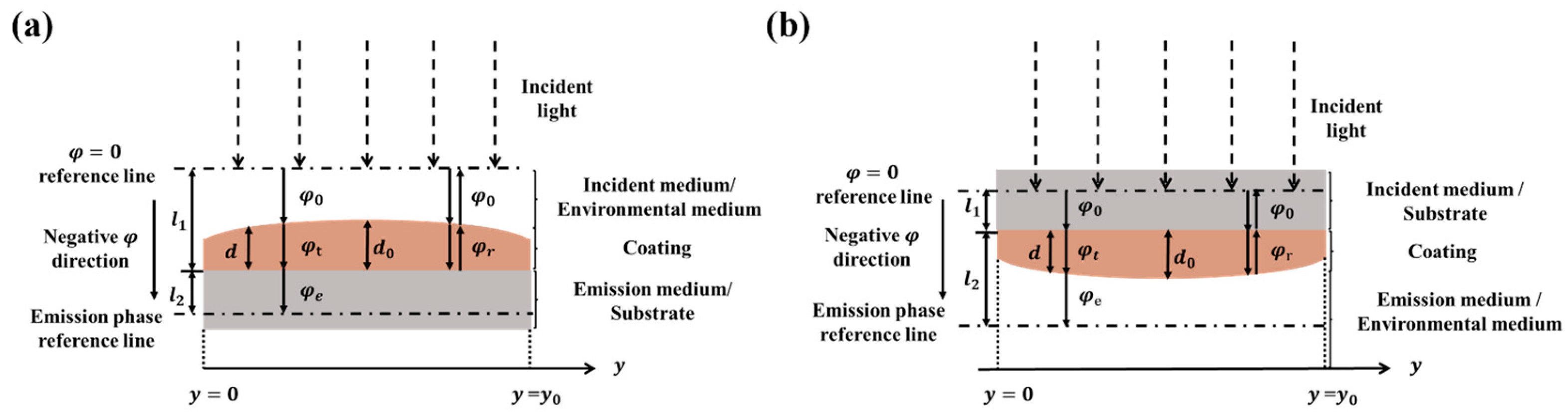
Figure 1 illustrates the wavefront errors caused by thickness non-uniformity in the optical coating system, demonstrating the interaction of light rays with an uneven optical multilayer coating surface. It is important to note that this study does not address wavefront errors resulting from bending induced by substrate stress.
The phase change of light after passing through an optical coating consists of two components: one resulting from phase changes as the light propagates through the environmental medium and another due to the phase shift occurring as the light travels within the coating system. Taking the reflective coating in
Figure 1a as an example, we study the wavefront errors caused by coating thickness non-uniformity. After reflecting off an optical multilayer coating, the light’s phase is determined by
In the equation above,
denotes the wavelength of the incident light. The phase shift introduced by the beam in the environmental medium can be expressed by the following equation, where
and
represent the incident angle of the light ray and the refractive index in the incident medium, respectively:
The characteristic matrix of the coating system indicates that the phase shift attributable to the coating is
and
are determined by Equation (4), where
represents the phase thickness, determining the change in the phase of light after it traverses the optical coating, as illustrated in Equation (5).
,
, and
, respectively, represent the optical admittance for the oblique incidence of the incident medium, coating layer, and emission medium.
The following section presents the formula for calculating optical admittance in various media and substrates with different polarization states. Here,
represents the refractive index of the medium,
indicates the angle of refraction within the medium, and
denotes the optical admittance of free space, approximately valued at
.
Therefore, the reflected wavefront error (
), after passing through an inhomogeneous optical coating, is expressed by the following formula, where
denotes the thickness error:
In optical coatings composed of layers with varying refractive indices, is characterized by the uniformity distribution across different materials. To simplify calculations, all materials are assumed to have the same relative uniformity distribution. Under this assumption, the thicknesses of each layer in the optical coating are scaled at various geometric points by a factor of . Thus, is the indicator for assessing the unevenness of the coating layer’s thickness.
First, let us begin the theoretical derivation by expanding
using Taylor’s expansion formula. Since
is very small compared to
, we can only consider the first-order term. Equation (7) can be expressed as
It is assumed that the thickness change ratio for each membrane layer in the system follows the adjustment factor
. Consequently, the proportional change in the thickness of each layer is consistent with the proportional change in the overall thickness of the membrane layers, as shown in the following equation:
Calculate the derivative of the phase with respect to thickness in Equation (8).
The slope of the phase change is calculated with respect to the wavelength without considering the dispersion of the incident medium and the emission medium.
It can be inferred that the relationship between the rate of phase change as a function of thickness and the rate of phase change [
29] as a function of wavelength is
In the formula above,
is a term related to the optical dispersion of the coating system, and it is approximated as 1 [
29], where
It can be derived from Equation (11).
The equation above states , which denotes the reflection group delay (.
Equation (14) is substituted into (8), considering the speed of light
, and
’s unit is fs. Considering the case in
Figure 1a, the difference between the transmission phase shift and the reflection phase shift arises solely from the different optical paths in the incident medium. We can derive Equation (15) as follows [
29,
30]:
denotes the transmitted wavefront error. The equation above states , which denotes the transmission group delay. Terms (a) and (b) represent the reflected and transmitted wavefront errors.
Next, consider the case of the reflective film illustrated in
Figure 1b. The phase of the light, upon reflection from an optical multilayer coating, is determined by
In the case of
Figure 1b,
is a constant for different geometric positions. The reflected wavefront error can be expressed by the following formula:
Employing a derivation process analogous to that used for Equation (8), we can deduce
Substituting the above expressions, we obtain
In the case of the transmissive film illustrated in
Figure 1b, the phase of light is determined by
The phase shift induced by the light propagating through the emission medium can be quantified by the following equation:
In the equation above,
and
denote the refractive angle of the light and the refractive index in the emission medium. The emission medium in
Figure 1b is also the environmental medium (typically air), corresponding to the incident medium in
Figure 1a; therefore, the meanings of
and
in
Figure 1b are the same as
and
in
Figure 1a. Similarly, the transmitted wavefront error shown in
Figure 1b can be expressed as
The above equation indicates that the uniformity error α and group delay () both affect the wavefront error. Furthermore, utilizing the equations, one can assess and optimize the wavefront performance of broadband optical multilayer coatings at a single operational angle.
From the formula above, it is evident that the same optical coatings display variations in wavefront performance across different wavelengths owing to the inherent
characteristics. This introduces a challenge: when wavefront tests are conducted on optical multilayer coating components at wavelengths outside their designed range without prior optimization of the coating system’s
, the results are frequently unreliable [
30]. Moreover, significant thickness uniformity errors often result in disproportionately magnified wavefront errors in optical multilayer coatings. Consequently, enhancing the overall imaging performance of optical coating components in high-precision optical systems necessitates minimizing thickness uniformity errors during manufacturing.
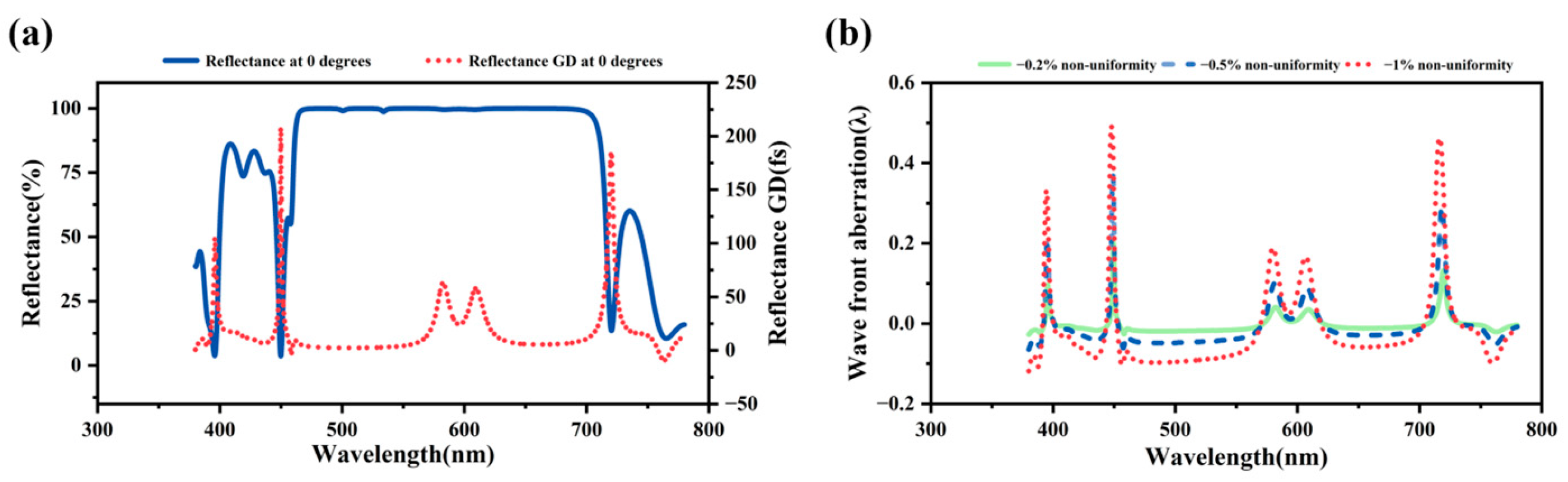
To substantiate the perspective discussed, this study employs the low-refractive-index material SiO
2 and the high-refractive index material TiO
2 to design optical coatings exhibiting reflectivity exceeding 98%, with a reflection band spanning 470–680 nm.
Figure 2a demonstrates the variations in the reflectivity and
properties of the mirror across wavelengths.
Figure 2b shows wavefront errors within the coating system across a range of wavelengths, determined by applying Equation (7). These errors are attributed to thickness non-uniformities with values of
,
, and
. The wavefront errors are quantified using peak-to-valley (PV) values.
The figure above shows that at wavelengths with a lower , the wavefront error of the coating is reduced. However, at a higher , phase shifts due to thickness non-uniformity significantly increase the wavefront error, consequently degrading image quality. Furthermore, the resultant wavefront error is proportionately amplified as thickness non-uniformity increases. Therefore, to guarantee that coating components in high-precision broadband imaging systems meet wave aberration requirements across all operating wavelengths, it is crucial to adjust the process parameters to enhance coating thickness uniformity and optimize the across the design spectrum.
To verify the accuracy of the wavefront error theory attributed to thickness non-uniformity, the wavefront aberrations of a thin-film system exhibiting a non-uniformity of
were evaluated by comparing the predictions of Equations (15), (19), and (22) with those from thin-film matrix theory (Equation (7)). Assuming a value of
in the calculations, these results are presented in
Figure 3. Across the entire wavelength range, the results from both methods coincide well, except in regions of
with large gradients, where the wavefront aberrations calculated by the simplified formula deviate from those derived using matrix theory. Typically, these wavelength bands lie outside the designed spectral range. This confirms that the earlier proposed Equations (15), (19), and (22) reasonably evaluate the wavefront errors induced by the thin-film system.
To achieve low wavefront errors across a broad bandwidth in high-precision optical systems, thin-film components operating at a single angle must simultaneously satisfy criteria and high-uniformity requirements. The achievement of primarily depends on the coating system’s design, whereas the coating’s uniformity depends on the precision of the equipment and the coating process. Wavefront errors arising from thin-film components working at a single wavelength typically display a non-uniform distribution, which can largely be compensated by alignment. Under broadband conditions, varies across different wavelengths, resulting in wavefront error variations, namely chromatic aberrations, which are generally challenging to compensate for solely through alignment. Consequently, it is crucial for thin-film components operating at a single angle within high-precision optical systems to fulfill the criteria and high-uniformity requirements to achieve low wavefront errors across a broad bandwidth.
3. Theoretical Analysis of Wavefront Error Under Wide-Angle Working Conditions
In this section, we study the interaction between wavefronts and optical coatings over a wide range of incident angles, assuming no thickness non-uniformity in the optical coatings, as illustrated in
Figure 4 above.
In polychromatic high-precision imaging systems equipped with high-numerical-aperture (NA) microscope objectives, the wide range of incident angles increases the system’s complexity. The phase of light varies with the wavelength, leading to different phase responses in the coating system and consequently generating chromatic aberrations. In these systems, wavefront aberrations primarily impact image quality.
The reflection phase of optical coatings at a wide range of incident angles can be calculated using the optical coatings matrix theory.
The formula for calculating
across a wide range of incident angles (not considering coating thickness non-uniformity) is as follows:
By employing a derivation process analogous to that in
Section 2, an analytical expression for wave aberration across a wide range of incident angles can be derived. The derivative of the reflection phase with respect to the incident angle can be expressed as follows:
By utilizing Equations (11) and (26), the following expression is derived:
In the above equation,
is defined as
If taking no account of optical dispersion of coating material,
In the equation above, and denote the coating materials’ highest and lowest refractive indices, respectively, and and denote the respective refractive angles. When the working angle is below 30 degrees, the ratio of the maximum to minimum values of is less than 3.
Equation (26) can be reformulated as follows:
Therefore, for optical coatings operating over a wide range of incident angles, is positively correlated with wavefront aberration. The above derivation process is also suitable for .
To verify the accuracy of the above-derived theoretical formulas, we use the typical coating system in
Section 2 as an example.
Figure 5 demonstrates the comparison between wavefront aberrations calculated using thin-film matrix theory and the derived formulas. The results calculated by the two different methods are very consistent.
According to Equation (23), the phase change of the coating system depends on the thickness of each coating layer and the angle of incidence. As the angle of incidence changes, the incident admittance for different wavelengths and polarization varies, thereby affecting the phase of the reflected light. This section further analyzes the typical coating system described in
Section 2. Utilizing thin-film matrix theory and Equation (24), this study calculates the reflected wavefront aberrations for incidence angles between 0 and 30 degrees at 520 nm and 610 nm wavelengths, each characterized by either a very low or higher
, facilitating contrastive analysis. The findings are presented in
Figure 6 below.
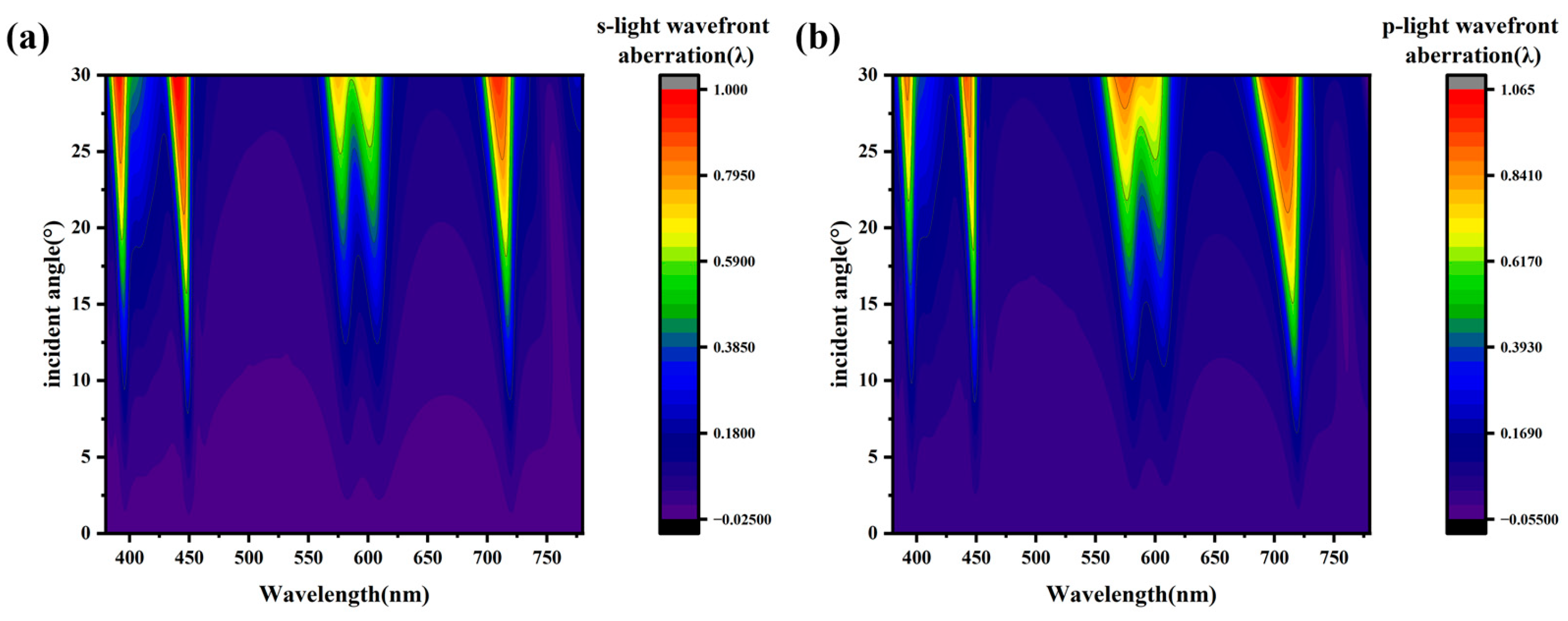
As demonstrated in
Figure 6, even in ideally uniform optical coatings, wavefront aberrations occur at a wide range of incident angles. Crucially, wavefront errors vary across different wavelengths. This indicates that optical coatings display dispersive properties under a wide range of incident angle conditions. Furthermore, these properties cannot be compensated for during assembly and alignment. If not optimized at the design stage, wavefront errors in the coating system will inevitably lead to a further deterioration of imaging quality.
Considering that peak-to-valley wavefront aberration values due to a wide range of incident angles at different wavelengths can yield wavefront aberration data throughout the passband, they can be calculated using Equation (24), with the results displayed in
Figure 7 below.
The diagram clearly shows that at a narrow range of incident angles, the wavefront error introduced by the optical coatings is minimal. However, as the range of incident angles increases, the wavefront error introduced by the film system gradually increases. Additionally, the introduced wavefront aberration is positively correlated with ; the greater the , the larger the introduced wavefront aberration. Therefore, it is recommended that the of the film system be minimized within the designed wavelength range to reduce the wavefront error across the entire bandwidth, thereby enhancing the performance of the multicolor high-precision imaging system.
In high-precision optical systems, thin-film components functioning over a wide range of incident angles yield varying phase responses due to the incidence of light at diverse angles, resulting in wavefront errors. In broadband optical systems, light with varying wavelengths provokes distinct responses, complicating the compensation for wavefront errors and chromatic aberrations caused by thin-film components through optical design and adjustments alone. Consequently, in broadband optical systems, minimizing the of coating systems is essential during the design of thin-film components to mitigate the resultant wavefront errors and chromatic aberrations. Meanwhile, to minimize wavefront errors introduced by complex coating systems over a wide range of incident angles and to meet the desired group delay () requirements, it is often necessary to reduce certain spectral specifications, such as transmittance and reflectance. Coating designers must evaluate and balance the relationship between wavefront errors and spectral performance.
4. Comprehensive Analysis of Wavefront Errors Induced by Optical Coatings
Now, let us consider a common scenario in actual optical systems where multilayer films exhibit a wide range of incident angles and coating non-uniformity. In systems particularly sensitive to aberrations, such as high-numerical-aperture (NA) microscope objectives or photolithography lenses, aberrations caused by optical coating components gradually become a major component of system aberrations. Thus, a comprehensive analysis and optimization are required for aberrations induced by antireflection coatings, light-splitting coatings, and reflective coatings on optical components. This section will take the previously mentioned typical stack of reflective coatings as an example to provide a comprehensive analysis of the wavefront errors introduced by this coating system in practical scenarios.
In subsequent analyses, wavefront aberrations in optical coating elements with a thickness non-uniformity of
are calculated using the optical coatings matrix theory, according to Equation (32). Considering the operational conditions of the optical coatings, incident angles from 0 to 30 degrees are displayed in
Figure 8. After accounting for thickness non-uniformity, the reflected wavefront error analysis of multilayer coatings over a wide range of incident angles reveals chromatic aberrations within the actual coating system. At wavelengths with a lower reflection group delay (
), such as 520 nm, the aberrations induced by optical coatings are smaller.
Using our current project as an example, we present a dielectric reflective coating for an immersion catadioptric microscope objective with a high numerical aperture (NA 1.0). Due to the high-power laser illumination used in the microscope objective, the metallic coating on the reflective surfaces (R1 and R2) will induce thermal strain, resulting in significant wavefront aberrations. Consequently, we need to coat the reflective surfaces with dielectric internal reflective films. The reflected wavefront errors on these surfaces must satisfy the requirement of
within the incident angle range of
and wavelength range of 550 nm–700 nm. The structural diagram of the microscope objective is illustrated in
Figure 9.
According to
Section 2, the wavefront error caused by thickness non-uniformity can be calculated using Equation (17). When the thickness non-uniformity
is
, considering only the wavefront error introduced by thickness non-uniformity, the
should be less than 35 fs to meet the wavefront error criterion.
According to
Section 3, even in the absence of thickness non-uniformity, the optical coating will still produce wavefront errors and chromatic aberrations when the incident angle range is large. To satisfy the reflected wavefront error requirement of
, the
should be less than 5 fs.
Consequently, compared to the coatings used at a single angle, the coatings applied over a wide range of incident angles could require significantly smaller under the same wavefront error specifications.
Following the systematic analysis presented earlier, optical coatings can be classified according to different application scenarios, thereby guiding the design and preparation of the coating systems. In the design of thin-film components for illumination and other optical systems, where aberration requirements are less stringent, the primary focus is placed on spectral characteristics, such as transmittance and reflectance. Consequently, potential wavefront errors introduced by these components are typically disregarded.
In high-precision optical systems, wavefront errors and chromatic aberrations introduced by thin-film components may be crucial factors that cannot be overlooked. Thin-film components are classified based on their operational contexts.
- (1)
Narrow wavelength and narrow incident angular ranges
These components experience wavefront errors primarily due to phase shifts caused by uneven thickness. The aberrations (such as defocus and spherical aberrations) induced by rotationally symmetric non-uniformity can typically be corrected through manufacturing and alignment processes. Therefore, and thickness uniformity are not the primary concerns in these coating systems.
- (2)
Narrow incident angular range and broadband conditions
When the coating thickness is ideally uniform, light entering at a narrow range of incident angles does not result in significant wavefront or chromatic aberrations. However, significant phase-shift differences across various wavelengths due to non-uniform coating thickness can lead to substantial chromatic aberrations, which are challenging to correct. As a result, during design and fabrication, the should be optimized considering the current process conditions of non-uniformity (Equation (15)) to minimize wavefront errors in broadband optical components.
- (3)
Narrow wavelength and wide incident angular range
When operating across a wide range of incident angles, thin-film components may exhibit wavefront errors due to phase differences caused by varying angles of incidence, even when the coating thickness is ideally uniform. Although wavefront errors can be partly compensated through manufacturing and alignment, the remaining wavefront errors can still be significant. Consequently, the design of thin-film systems should minimize the across a broad range of angles.
- (4)
Wide angular range and broadband wavelength
Dispersion effects arising from phase shifts across a wide range of incident angles pose significant challenges in correcting wavefront errors and chromatic aberrations through manufacturing and alignment processes. Therefore, it is essential to minimize the within the operational bandwidth of the thin-film system and to mitigate thickness non-uniformity by optimizing process parameters, thereby reducing wavefront errors and chromatic aberrations attributable to the thin-film components.
