1. Introduction
The advent of photonic integrated circuits (PICs) is poised to disrupt conventional communication, data processing, and sensing paradigms. By synergistically merging photonic capabilities with microelectronic expertise, PICs have the potential to transform the landscape of optical computing [
1,
2,
3]; as a result, they offer unparalleled speed and efficiency in communication. The scalability of PICs is further enhanced by their conformity to the CMOS fabrication process. This compatibility enables the creation of highly energy-efficient PICs [
4], making them increasingly attractive for a wide range of applications. Recent advances have demonstrated high-performance, polarization-insensitive waveguide crossings with various design strategies [
5,
6]. Optical switches, quantum photonics devices, and superconducting optoelectronic circuits [
7] rely heavily on waveguide crossings to route light efficiently. In these applications, waveguides crossings are used to direct light from input ports to output ports or combine signals from multiple sources. By using polarization-insensitive waveguide crossings in silicon photonics, researchers can integrate polarization-division-multiplexing (PDM) technologies, thereby increasing optical link capacity while minimizing power consumption and losses associated with signal degradation. Silicon photonics may be augmented by the incorporation of polarization-insensitive waveguide crossings, thereby facilitating the integration of PDM technologies and yielding a substantial increase in optical link capacity while concurrently reducing power consumption.
The manipulation of polarization modes is foundational for the operation of high-performance polarization-handling devices, such as polarization beam splitters (PBSs), polarization rotators (PRs), and polarization splitter-rotators (PSRs). This phenomenon plays a pivotal role in enabling polarization-transparent photonic integrated circuits (PICs), as well as advancing coherent optical communication systems and multidimensional quantum communication protocols [
7,
8]. Several schemes have been developed to achieve polarization independence in photonic devices. For example, ref. [
9] explored advanced polarization management techniques in photonic beam splitters, while the study in ref. [
10] presented an innovative approach for creating highly efficient polarization rotators utilizing multi-mode waveguides. These references highlight key advancements in achieving polarization-independent functionality within integrated photonics. In addition to polarization independence, the miniaturization of photonic devices has garnered attention for its role in advancing compact integrated photonic circuits. Various ultra-compact functional device schemes have been proposed to meet the demands for reduced device footprints while maintaining a high performance. Notably, refs. [
11,
12] explored optimized methods for achieving high-density multi-mode photonic integration. Additionally, there have been some notable attributes to demonstrate high-performance polarization-insensitive waveguide crossing, with examples including the utilization of parallel crossing waveguides, as demonstrated in refs. [
13,
14]. This design approach has proven particularly advantageous for achieving increased compactness, particularly in scenarios where input or output waveguides are originally parallel and situated near one another, a common occurrence in various applications. In ref. [
15], a device with measured insertion loss as 43 ± 4 mdB per crossing with crosstalk of <−50 dB was reported. Waveguide crossing reported in ref. [
16], combining multi-mode interference (MMI) and a mode division multiplexer (MDM), has a footprint of 4.8 μm
2 × 4.8 μm
2 and an insertion loss of 0.6 dB and −24 dB from 1530 nm to 1590 nm for both
and
modes, respectively. Researchers in [
17] successfully fabricated a compact, polarization-insensitive silicon waveguide crossing on the 220 nm SOI platform, which exhibits a commendable performance, including insertion loss (<1 dB), polarization-dependence loss (<0.6 dB), and crosstalk (<−35 dB) for both TE and TM polarizations, with a footprint of 12.5μm × 12.5 μm. However, despite these advancements, developing scalable, multi-mode waveguide crossing solutions that balance compactness, low insertion loss, and minimal intermodal crosstalk remains an ongoing challenge in the field. Existing solutions often face trade-offs between device performance and design complexity, which limits their applicability in more complex PICs and high-density integration scenarios.
By combining the finite difference time domain (FDTD) method, a powerful numerical tool for simulating electromagnetic phenomena, with advanced inverse optimization algorithms, it is now possible to transcend the limitations imposed by traditional design expertise, thereby enabling the creation of highly compact, integrated silicon components. The increasing sophistication of inverse design methodologies in nano-fabrication has led to the development of highly intricate optical structures on photonic chips. This breakthrough has profoundly impacted the miniaturization of photonic devices, as evidenced by a plethora of studies [
18,
19,
20,
21,
22,
23]. By seamlessly integrating metamaterials and subwavelength structures onto chip substrates, it has become possible to harness novel degrees of freedom in controlling light propagation, thereby unlocking entirely new avenues for on-chip optical manipulation. Contrary to forward design methods, which rely heavily on the domain knowledge and experience and present challenges in designing multiple refractive-index states within a single geometry, the inverse design method utilizes various iterative optimization techniques. These methods expand the design space and autonomously identify optimal parameter combinations [
19,
24]. With the current state of inverse design in nanophotonics, it is now possible to efficiently drive the miniaturization of photonic devices, seamlessly integrating metamaterials and subwavelength structures onto chip substrates, while also providing unprecedented flexibility in controlling light propagation [
19,
20]. ref. [
25] employed a hybrid global optimization approach using a physics-informed generative adversarial network combined with a refinement algorithm for the design of polarization-insensitive waveguide crossings. While effective, this study introduces a distinct optimization strategy aimed at enhancing computational efficiency and compactness
This study exploits the mirror symmetry direct binary search (DBS) methodology to demonstrate an ultra-compact and low-loss polarization-insensitive silicon waveguide crossing. A specifically designed waveguide crossing, featuring a diminutive footprint of 3 × 4 μm2, has been optimized for operation within the 1530~1570 nm spectral band. Notably, this design achieves remarkably low insertion losses (<−0.11 dB) and crosstalk levels (<−22.6 dB) in the transverse electric (TE) mode, as well as even lower losses (<0.05 dB) and crosstalk levels (<−24.5 dB) in the transverse magnetic (TM) mode. The results present that the proposed mirror symmetry along both the X-axis and Y-axis optimization produced ultra-low loss devices while saving optimization time. The compact footprint, ultra-low insertion loss, and straightforward fabrication steps of our proposed designs render them highly desirable for large-scale and high-density photonic integration applications.
2. Designs and Methods
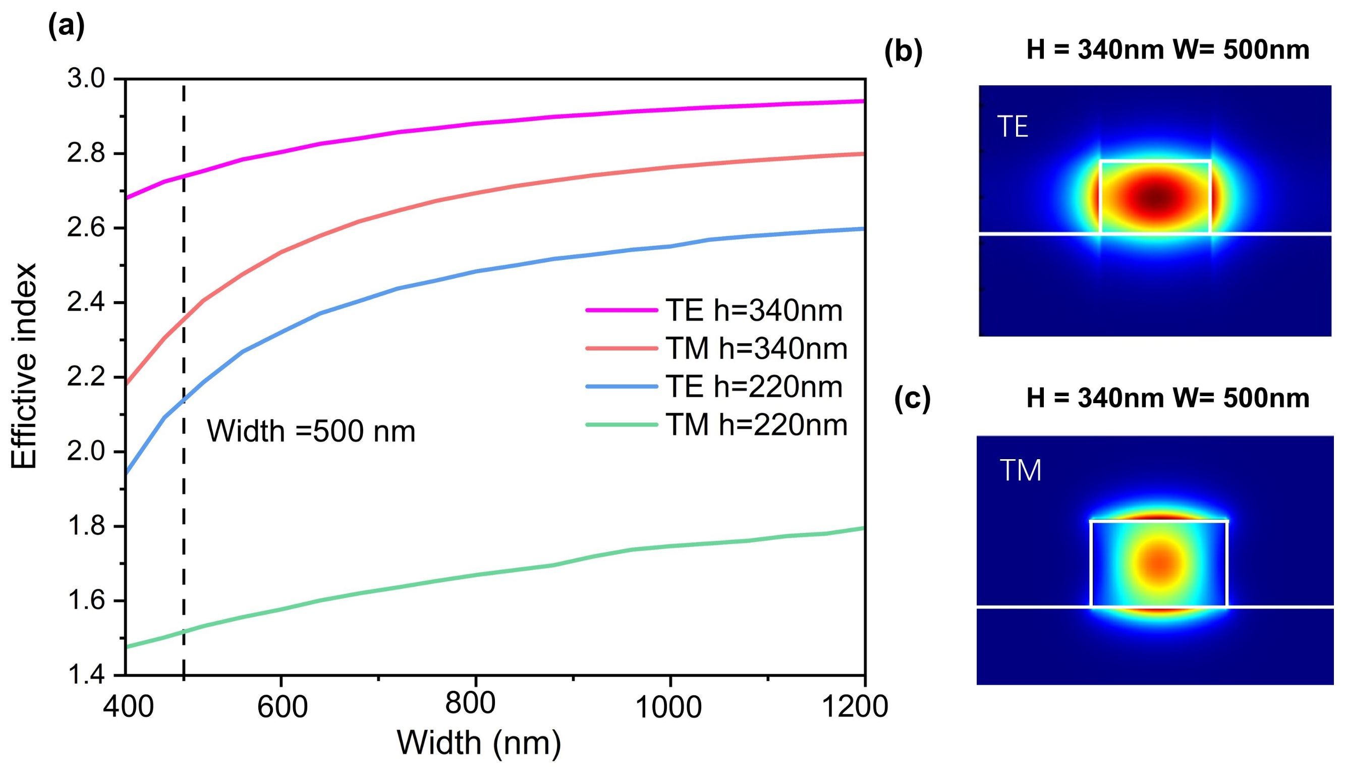
To begin with, we implement a structure on a 340-nm-thick top silicon-on-insulator (SOI) platform. The choice of a 340 nm SOI platform is particularly advantageous for achieving polarization insensitivity due to its improved control over both transverse electric (TE) and transverse magnetic (TM) modes. As illustrated in
Figure 1, the effective indices of the fundamental TE and TM modes vary as a function of the waveguide width at a wavelength of 1550 nm. Compared to the 220-nm SOI, the 340-nm SOI can support multiple modes due to its greater thickness, making it suitable for multi-mode applications or scenarios requiring stronger light confinement. With a larger thickness, the waveguide can handle higher power for the same waveguide dimensions, which is better for the polarization-insensitive waveguide crossing scenario. According to the research, the 340-nm SOI platform is more suitable for polarization-insensitive situations, for example, the 340 nm-SOI platform is more widely used in designing multi-mode multiplexing devices like PDM and MDM, for example, splitters [
26] and phase shifters [
27]. Furthermore, the greater thickness of the 340 nm SOI supports multiple modes, enhancing light confinement and allowing the waveguide to handle higher power without affecting its dimensions, making it ideal for multi-mode applications. Taking into account the practical application scenarios and aiming to make our designed waveguide devices more compatible with other devices, we chose to use 340 nm SOI platforms to design the waveguide crossing devices with different functions.
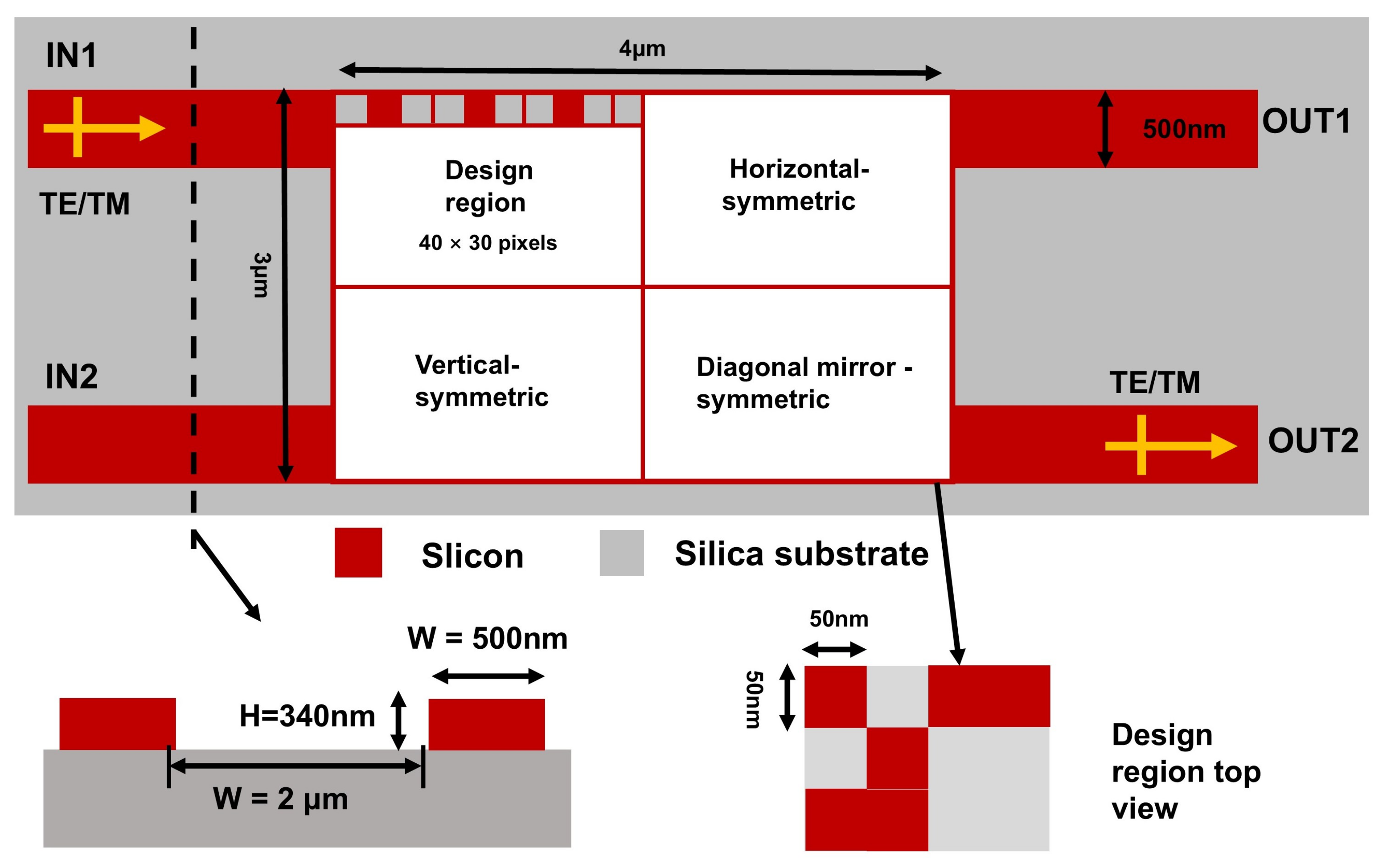
The ultra-compact
polarization-insensitive silicon waveguide crossing is depicted in
Figure 2, which is designed on a SOI platform featuring an individual 340 nm thick silicon core layer. The device consists of two input and two output waveguides, with the design region incorporating a one-fourth waveguide crossing structure. Notably, the width of both the input and output waveguides is set to 500 nm, while the distance between the upper and lower waveguides is 2μm. The total size of the design area measures 2 × 1.5 μm
2. The coupling region structure of the device is composed of discrete square pixels, in which the red part is the silica layer and the gray part is the silicon layer. This square pixel design is chosen for its simplicity and efficiency in the optimization process, as well as ease of fabrication. To achieve an optimal design for the ultra-compact polarization-insensitive silicon waveguide crossing, the mirror symmetry direct binary search (DBS) algorithm was applied to a design region comprising 30 × 40 pixels. The waveguide crossing structure consists of 60 × 80 pixels of 50 nm × 50 nm, the permittivity
of each pixel in the design area can have either the value of the background permittivity
or the material permittivity
. To achieve the mirror symmetry along both the X-axis and Y-axis, as well as horizontal, vertical, and diagonal mirror symmetries required for the ultra-compact polarization-insensitive silicon waveguide crossing, the design region was divided into a grid of 30 × 40 grid of pixels. These symmetry constraints play a crucial role in reducing the complexity of the optimization process. Specifically, by enforcing mirror symmetry, the design space is reduced from the original 4800 pixels to only 1200 independent pixels that need to be optimized. This significant reduction in the search space streamlines the optimization and enhances computational efficiency while ensuring that the final design remains polarization-insensitive. At every iteration of the direct binary search, the pixel values are updated while maintaining this mirror symmetry, meaning that changes to one pixel are mirrored across the entire structure according to the symmetry rules. This reduces the degrees of freedom in the optimization, allowing the algorithm to efficiently explore viable designs that satisfy both performance and symmetry requirements. While this approach ensures a balanced design for the polarization-insensitive waveguide crossing, its use of symmetry also streamlines the pattern generation process in electron-beam lithography (EBL), contributing to a more efficient and predictable fabrication process.
When a pixel switches its state, the symmetrical area corresponding pixel state changes and a figure of merit (FOM) is calculated. The FOM for the optimization is defined as
Here,
is the average transmission energy, as
and
in the wavelength range of 1530~1570 nm are input from the In1 port. As depicted in
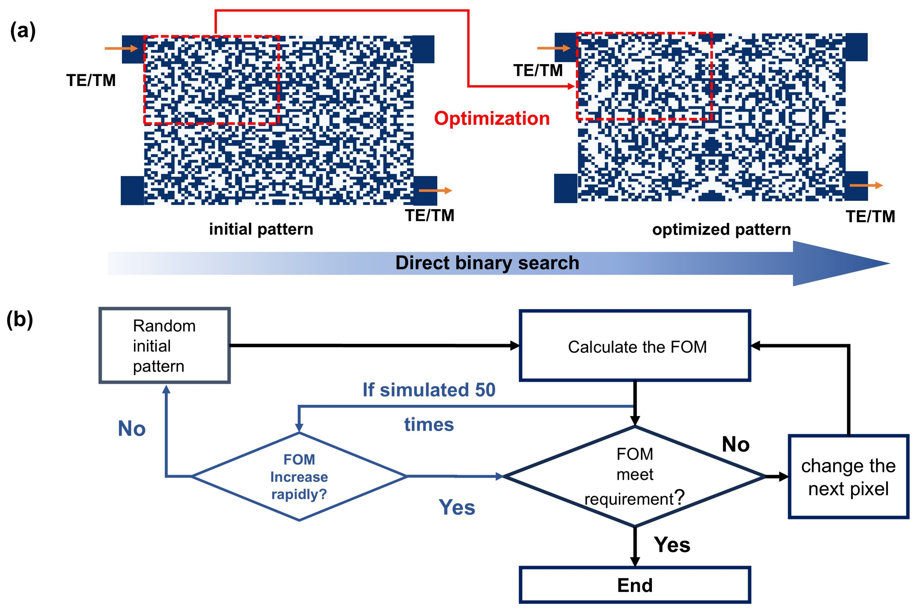
Figure 3b, the direct binary search (DBS) algorithm proceeds through an iterative refinement process. During each iteration, each pixel within the design is evaluated twice: once with a ‘0’ state and once with a ‘1’ state. The state of the pixel is updated based on the figure of merit (FOM), which assesses the design’s optical performance. If changing the pixel’s state improves the FOM, the new state is retained. Otherwise, the pixel is reverted to its original state, and the algorithm moves on to the next pixel. This process repeats until all pixels have been evaluated, marking the completion of a single iteration. Throughout each iteration, the algorithm systematically searches for the optimal binary pattern that meets the desired optical properties by toggling the states of individual pixels. The mean transmission energy is used to evaluate the performance of the polarization-insensitive waveguide crossing. By iteratively adjusting pixel states, the DBS algorithm refines the design to enhance the FOM. In our approach, a key aspect is the implementation of a mirror symmetry constraint within the DBS algorithm. During each iteration, random toggling of pixel states between ‘0’ and ‘1’ is performed while maintaining this mirror symmetry, ensuring that any adjustments to the pixel layout adhere to the symmetry rules of the waveguide design. This constraint not only simplifies the search space, but also optimizes the design to achieve polarization-insensitive performance. The iterative process continues until all pixels have been toggled and evaluated, resulting in the completion of one full refinement cycle. An additional iterative step has been incorporated into the design workflow to refine the spectral response, involving an enhanced initial pattern selection procedure. To gauge the sensitivity of our DBS algorithm, we experimented with diverse initial patterns, simulating numerous scenarios. Upon observing little variation in FOM values after 50 iterations, we terminated the simulation and opted for an alternative random pattern to uncover potential initial configurations. Our reliance on a symmetrical pattern enables a more expeditious optimization process, thereby significantly enhancing the efficiency of the initial pattern selection.
The efficacy of our devices is gauged through two critical performance metrics: insertion loss (IL) and crosstalk (CT). Insertion loss, a measure of signal attenuation, is quantified as follows:
Here,
represents the optical power at the target output port which is the out2 port, while
denotes the incident input power from the in1 port. Conversely, crosstalk, a manifestation of signal leakage, is defined as follows:
In this context, corresponds to the optical power at non-target output ports, including the leaking light through the port out2 and in2, and the reflected light from the input port in1. represents the incident input power. Notably, both IL and CT values should remain equivalent across all ports, given the central symmetry of our crossing design.
3. Results
Figure 4a presents the iterative results for the average transmission of TE and TM modes across the C band, revealing a rapid change in figure of merit (FOM) after 50 iterations. This observation suggests that the random initial pattern employed may serve as a promising starting configuration, prompting the optimization loop to continue rather than terminating prematurely. Here, the transmission of TE and TM is the figure of merit (FOM) of the TE mode and TM mode, respectively, during the iteration, which is defined as:
and
. Notably, for the chosen initial setup, the transmission for the TE mode (
) gradually increases over 250 iterations of the optimization process, ultimately converging to a stable solution. To evaluate the true effectiveness of our approach,
Figure 4b further illustrates a direct comparison of the FOM changes between symmetric and non-symmetric DBS optimization methods. Notably, for the chosen initial setup of the non-symmetric DBS optimization scenario, the TE mode transmission (
) also gradually increases over the optimization process, but the convergence is notably slower compared to the symmetric optimization. While the non-symmetric method eventually stabilizes, it requires more iterations to achieve comparable results, as shown in
Figure 4b. In contrast, the proposed mirror-symmetric DBS optimization, combined with the randomly generated initial pattern obtained after 50 iterations, facilitates the efficient identification of an optimal solution. This approach reduces computational requirements and minimizes optimization time, as the symmetry reduces the search space, leading to faster convergence. The mirror symmetric DBS method achieves significantly faster convergence compared to the non-symmetric approach. This faster convergence is due to the reduced search space introduced by symmetry constraints, which directly impact the computational load by lowering the number of design parameters that need optimization. Unlike the hybrid global optimization of ref. [
25], which focused on leveraging a generative model to explore the global topology of potential device designs followed by DBS refinement, the present work employs a direct binary search algorithm with mirror symmetry constraints. This approach streamlines the optimization process by significantly reducing the search space through symmetrical constraints, thereby improving computational efficiency and minimizing design complexity. The schematic diagram of the proposed polarization-insensitive waveguide crossing is depicted in
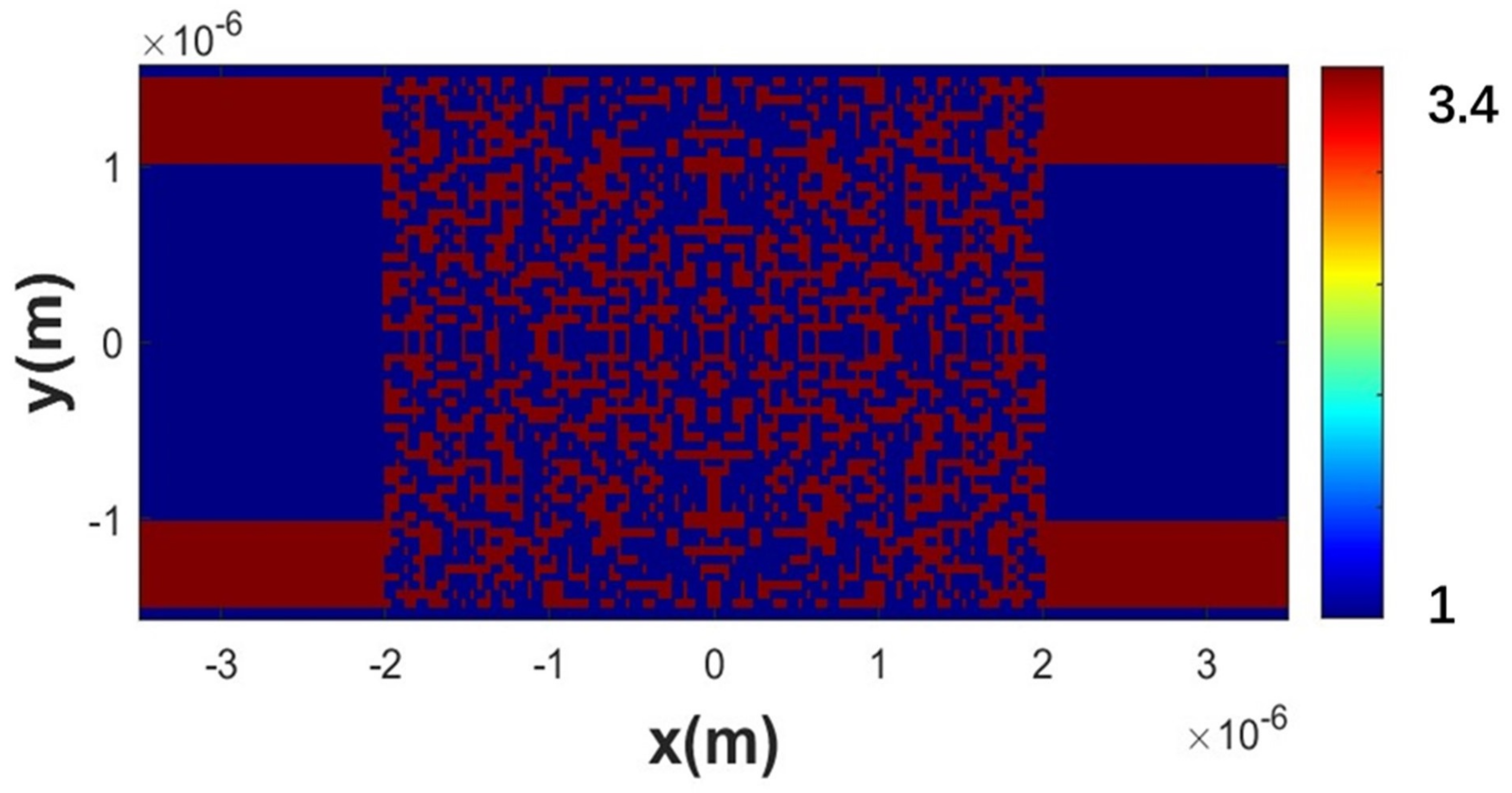
Figure 5.
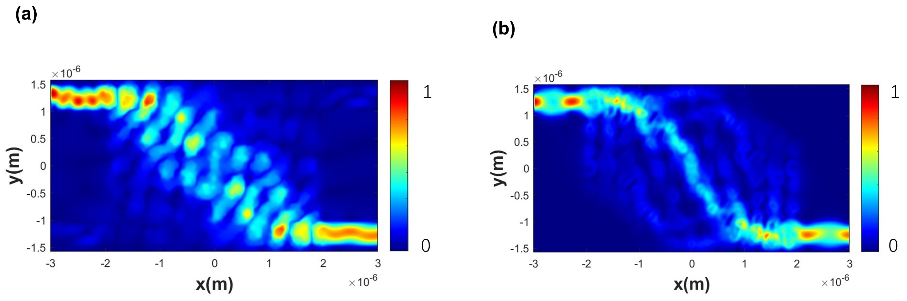
Figure 6 illustrates the behavior of incident light for the TE and TM modes as they enter the crossing area through the left port and propagate along the x-axis within the device. When inputting 1550 nm light from the input waveguide channel,
Figure 6a,b show the normalized optical intensity distributions for the TE and TM modes at a wavelength of 1550 nm, respectively. Most of the input energy is directed to the output port for both modes, with highly consistent and symmetrical light intensity distributions. The calculated transmission spectra of the polarization-insensitive waveguide crossing device (as presented in
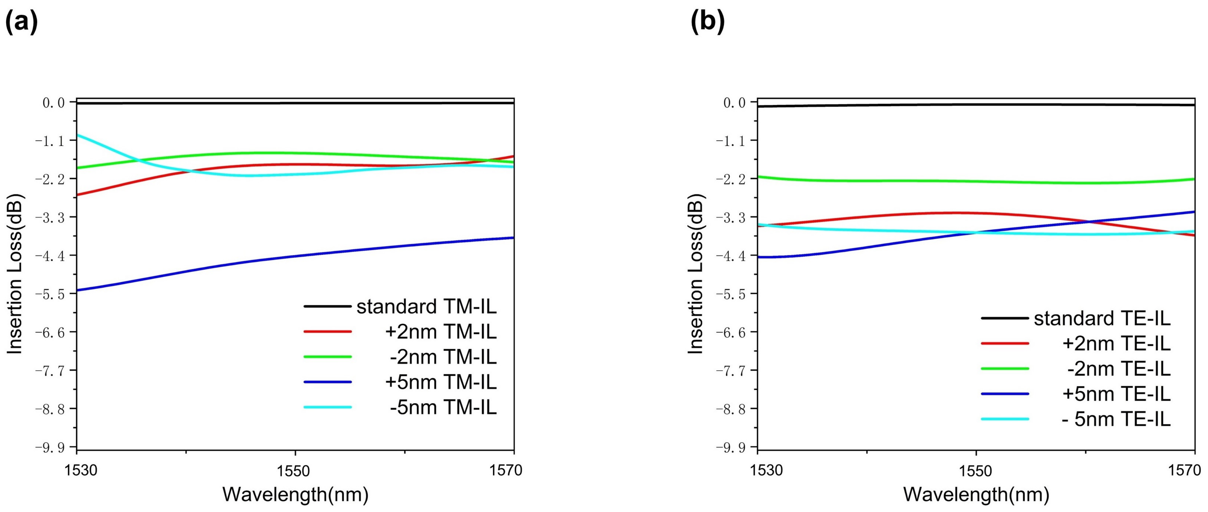
Figure 7) exhibit peculiarly flat spectral curves for insertion loss (IL) across the corresponding wavelength range, demonstrating its robust wavelength-insensitive behavior within the C-band. Specifically, at a wavelength of 1550 nm, the insertion losses (ILs) for the TE and TM modes are measured to be 0.047 dB and 0.08 dB, respectively. The calculated crosstalk (CT) for the TE and TM output ports at 1550 nm are 22.6 dB and 25.7 dB, respectively. Simulation results further show that both TE and TM modes exhibit low insertion losses (<0.05 dB for TE mode and <0.11 dB for TM mode) and excellent crosstalks in the range of 21~25 dB across a broad wavelength band of 40 nm, spanning the C-band (1530~1565 nm). This performance indicates that the device has great potential for integration with WDM on-chip systems to enhance link capacity.
Our design outperforms existing state-of-the-art polarization-insensitive silicon waveguide crossing structures in both transmission performance and compactness, as demonstrated by the comprehensive comparison presented in
Table 1. Specifically, when compared to [
28], our design achieves better insertion loss across the optical wavelength range and boasts a much smaller footprint. While the crosstalk of our design is slightly higher than that reported in [
28], the substantial reduction in device size makes our approach more attractive for compact photonic integrated circuits. Compared with [
29], our design has an identical crosstalk performance while offering a significantly reduced footprint, making it an ultra-compact solution. In conclusion, this work presents an ultra-compact polarization-insensitive waveguide crossing structure that excels in both transmission performance and device size. By leveraging advanced design techniques, we have successfully minimized the footprint of our device without compromising its effectiveness in supporting both TE and TM modes.
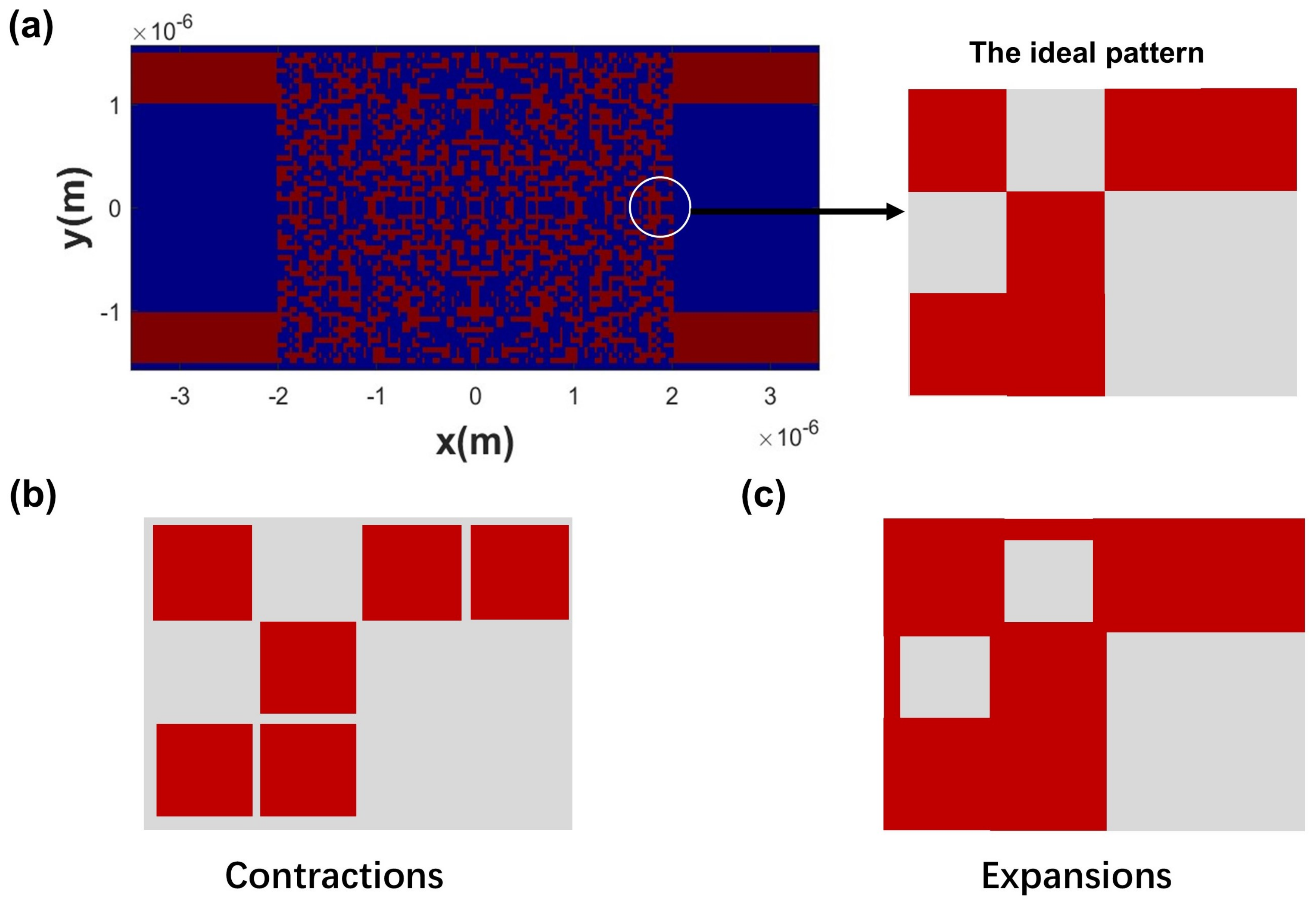
For sophisticated subwavelength devices, fabrication imperfections inevitably lead to a deterioration in insertion losses and crosstalks. To assess the resilience of our design, we subjected it to a simulation of device performance under diverse fabrication imperfections, encompassing pixel-related edge expansions or contractions of 2 nm and 5 nm, which accurately capture the minute distortions arising from the fabrication process. These devices could be fabricated on a 340 nm SOI wafer featuring a 2 μm buried oxide layer using electron-beam lithography (EBL) and inductively coupled plasma (ICP) etching.
Figure 8a shows the ideal design, with the pixelated layout representing the arrangement of etched and unetched regions. The zoomed-in section highlights a portion of the pattern with its intended geometry.
Figure 8b depicts a contraction scenario, where the red regions, representing silicon portions, are reduced by 2 nm or 5 nm. This can occur due to over-etching or other fabrication inaccuracies, leading to a reduced size of the features in the pattern.
Figure 8c shows an expansion case, where the red etched areas are enlarged by 2 nm or 5 nm. In the simulations, we found that contraction scenarios exhibit a slightly better performance compared to expansions for both TE and TM modes. This observation implies that with appropriate process control, the effect of fabrication imperfections can be mitigated.
Figure 9 illustrates how fabrication imperfections, specifically contractions and expansions of the structure, impact the waveguide crossing pattern.
The simulation outcomes are presented in
Figure 9, which demonstrates that both expansion and contraction errors give rise to mismatches in device lithography, resulting in the disappearance of regions originally intended for small dimensions. Notably, our simulations indicate that the contraction scenario exhibits a marginally superior performance compared to the expansion case for both devices, suggesting that it is more resilient to fabrication imperfections. Furthermore, with an acceptable insertion loss of <2 dB for the TM mode at 2 nm and 5 nm edge contraction, the degradation resulting from fabrication error remains tolerable within acceptable limits. In addition to the previously mentioned results, our results show that, alongside an insertion loss of less than 3 dB for the TE mode at 2 nm and 5 nm edge contraction, the affected areas exhibit tolerable diminutions in their TE mode waveguide crossing performances. These findings collectively demonstrate that our design exhibits a high degree of robustness against minor fabrication errors, underscoring its reliability as a viable option for compact photonic integrated circuits. While pixel-based designs are inherently more sensitive to fabrication errors, the results indicate that such deviations can be controlled effectively, and the tolerances are within the bounds needed for high-performance photonic devices.
4. Discussion
This study presents a compact and low-loss polarization-insensitive silicon waveguide crossing, achieved through the application of mirror symmetry-based direct binary search. Operating within the 1530~1570 nm wavelength regime, our design significantly advances the field by offering a remarkably small footprint of 3 × 4 μm2, achieving insertion losses as low as −0.11 dB for TE mode and below 0.05 dB for TM mode, with crosstalk levels below −22.6 dB and −24.5 dB, respectively. In comparison with previous designs, this polarization-insensitive waveguide crossing exhibits enhanced performance metrics. Moreover, by enforcing symmetry constraints, the search space is significantly reduced, which not only accelerates convergence but also minimizes the computational requirements. Future research could focus on further enhancing device compactness or exploring alternative optimization strategies, by handling multiple modes within a compact footprint; such devices can enable more efficient and flexible signal routing, thereby supporting the development of scalable and high-speed photonic circuits, which are critical for advancing integrated photonics.


