Communication

All-Dielectric Dual-Band Anisotropic Zero-Index Materials

1
College of Physics, Nanjing University of Aeronautics and Astronautics, Nanjing 210016, China
2
School of Physical Science and Technology & Jiangsu Key Laboratory of Frontier Material Physics and Devices, Soochow University, Suzhou 215006, China
*
Authors to whom correspondence should be addressed.
Photonics 2024, 11(11), 1018; https://doi.org/10.3390/photonics11111018
Submission received: 27 September 2024 / Revised: 28 October 2024 / Accepted: 28 October 2024 / Published: 29 October 2024
(This article belongs to the Special Issue Advances in Epsilon-Near-Zero Photonics)

Abstract

:
Zero-index materials, characterized by near-zero permittivity and/or permeability, represent a distinctive class of materials that exhibit a range of novel physical phenomena and have potential for various advanced applications. However, conventional zero-index materials are often hindered by constraints such as narrow bandwidth and significant material loss at high frequencies. Here, we numerically demonstrate a scheme for realizing low-loss all-dielectric dual-band anisotropic zero-index materials utilizing three-dimensional terahertz silicon photonic crystals. The designed silicon photonic crystal supports dual semi-Dirac cones with linear-parabolic dispersions at two distinct frequencies, functioning as an effective double-zero material along two specific propagation directions and as an impedance-mismatched single-zero material along the orthogonal direction at the two frequencies. Highly anisotropic wave transport properties arising from the unique dispersion and extreme anisotropy are further demonstrated. Our findings not only show a novel methodology for achieving low-loss zero-index materials with expanded operational frequencies but also open up promising avenues for advanced electromagnetic wave manipulation.

1. Introduction

Zero-index materials (ZIMs), characterized by near-zero permittivity and/or permeability, represent a unique class of materials exhibiting extraordinary properties, such as infinitely long wavelengths and zero phase advancement [1,2,3,4]. These distinctive features have facilitated numerous novel phenomena and applications, including tunneling waveguides [5,6,7,8,9], radiation and flux control [10,11,12,13,14], photonic doping and anti-doping [15,16,17,18,19,20,21,22,23,24,25], the enhancement and quenching of optical nonlinearity [26,27,28,29,30,31,32,33], and zero Minkowski-canonical momentum [34], etc. ZIMs have been realized across a wide range of frequencies, spanning from microwave to terahertz, infrared, and visible spectra, through the use of plasmonic materials at plasma frequencies [26,35,36,37,38,39,40,41,42,43], non-resonant metal–dielectric composites [44,45], resonant metamaterials [7,14,24,46], waveguide metamaterials at cutoff frequencies [6,8,13,47,48], and photonic crystals (PhCs) [18,24,25,49,50,51,52,53,54,55,56,57,58], etc. Despite these achievements, most practical implementations of ZIMs rely on metallic components or plasmonic materials, leading to significant material losses at high frequencies.
Dielectric PhCs, displaying a Dirac-like cone at the center of the Brillouin zone due to accidental degeneracy of linear and flat bands, offer a promising approach to achieve effective ZIMs with negligible losses [18,24,25,49,50,51,52,53,54,55,56,57,58,59,60]. Low-loss ZIMs have been successively realized using silicon PhCs, holding potential applications in optical meta-waveguides and meta-devices [54,55,56,57,58]. Interestingly, introducing optical anisotropy to the PhC can transform a Dirac-like cone into a semi-Dirac cone, characterized by a linear-parabolic dispersion [60,61,62,63,64,65]. The PhC that possesses a semi-Dirac cone can be linked to an effective anisotropic zero-index material (AZIM), functioning as a double-zero material (with effective permittivity ε e f f = 0 and effective permeability μ e f f = 0 ) along specific propagation directions, but an impedance-mismatched single-zero material (with ε e f f = 0 or μ e f f = 0 ) along the perpendicular directions at the semi-Dirac-point frequency [60,61,62,63,64,65]. Notably, these AZIMs exhibit unique properties that are absent in isotropic ZIMs, such as arbitrary flux control [12,13], extreme field confinement due to skin effect of electromagnetic flux [14], and highly anisotropic wave transport properties [60,61,66], etc. However, the PhC-based ZIMs are usually limited to operating at a single frequency, i.e., the Dirac-point frequency or semi-Dirac-point frequency. Very recently, a three-dimensional PhC comprising metal–dielectric particles has been demonstrated to act as an effective AZIM at two distinct frequencies through the rare dispersion of dual semi-Dirac cones [66]. Nevertheless, the presence of metallic components still causes significant losses at high frequencies, and the realization of multi-frequency PhC-based low-loss ZIMs remains an open challenge.
In this work, we propose a kind of three-dimensional terahertz silicon PhC that exhibits dual semi-Dirac cones at two distinct frequencies, capable of functioning as effective dual-band AZIMs with negligible material losses. At the two semi-Dirac-point frequencies, the silicon PhC functions as an effective double-zero material along two specific propagation directions and as an impedance-mismatched single-zero material along the orthogonal direction. We further demonstrate the highly anisotropic wave transport property of the AZIM, i.e., drastically different transport properties for waves of different wave-vector directions at the two semi-Dirac-point frequencies, as a consequence of the unique dispersion and extreme anisotropy. These results introduce a novel approach for achieving low-loss AZIMs with expanded operational frequencies.

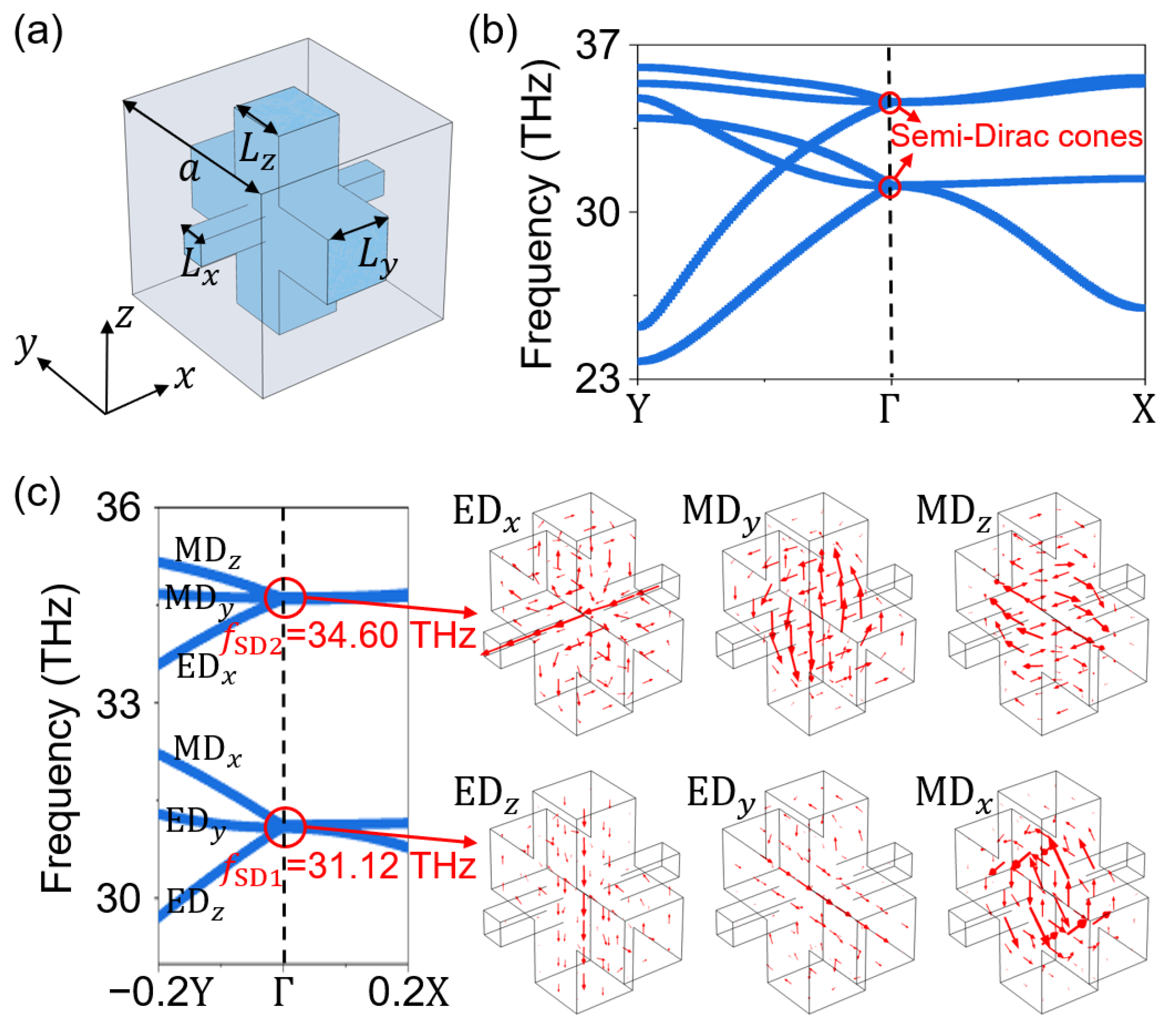
2. Silicon PhC with Dual Semi-Dirac Cones

Figure 1a shows the schematic graph of the proposed three-dimensional silicon PhC, composed of orthogonally aligned silicon rods. When all silicon rods are identical, the PhC exhibits O h lattice symmetry, which can be engineered to support a Dirac-like cone arising from the accidental degeneracy of four linear bands and two flat bands [24,25,26,66]. To introduce optical anisotropy into the PhC to reduce the structural symmetry to D 4 h , the size of the silicon rods along the x direction is modified. This symmetry reduction can transform the original Dirac-like cone into two semi-Dirac cones, separated in the frequency spectrum [66]. The resulting PhC, exhibiting dual semi-Dirac cones, can be effectively homogenized as a low-loss AZIM operating at two distinct frequencies, as illustrated in Figure 1b.
The unit cell of the three-dimensional silicon PhC is depicted in Figure 2a, consisting of orthogonally aligned silicon rods arranged in a cubic lattice with a lattice constant of a = 5   μ m . The relative permittivity of silicon was set to be 12, which can be considered dispersionless within the studied frequency range of 20–37.5 THz [67]. All silicon rods have square cross-sections, with side lengths of L x , L y , and L z corresponding to the rods aligned along the x , y , and z directions, respectively. Here, we set L x = 0.525   μ m and L y = L z = 1.5   μ m , indicating that the rods aligned along the y and z directions are identical.
The photonic band structure along the Γ X and Γ Y directions for the three-dimensional silicon PhC is computed using the finite-element software COMSOL Multiphysics, as presented in Figure 2b. Notably, two semi-Dirac cones are observed: the lower-frequency cone at f S D 1 = 31.12   T H z , referred to as the first semi-Dirac cone, and the higher-frequency cone at f S D 2 = 34.60   T H z , referred to as the second semi-Dirac cone. The detailed view of the band structure in the left panel of Figure 2c reveals that near each semi-Dirac-point frequency, the dispersion curves comprise two linear bands along the Γ Y direction, while two overlapped parabolic bands along the Γ X direction are tangent to a flat band at the semi-Dirac-point frequency.
To explore the characteristics of the degenerate modes at the semi-Dirac-point frequencies, electric-field distributions for these degenerate modes along the Γ Y direction are plotted as the frequency gradually increases near the semi-Dirac cones, as indicated by the arrows in the right panel of Figure 2c. It is observed that the dual semi-Dirac cones are the consequence of two sets of triply accidental degeneracy of electric dipolar (ED) and magnetic dipolar (MD) modes. An ED mode is characterized by oscillating electric fields along a specific direction, inducing a magnetic current loop, whereas a MD mode is characterized by an electric displacement current loop within the PhC unit cell, generating a MD moment orthogonal to the current loop [68]. For clarity, we label the ED (or MD) mode oriented along the i ( i x , y , z ) direction as the E D i (or M D i ) mode.
Specifically, the first semi-Dirac cone originates from the accidental degeneracy of two ED modes (i.e., E D z and E D y modes) and one MD mode (i.e., M D x mode). In contrast, the second semi-Dirac cone is the result of the accidental degeneracy of one ED mode (i.e., E D x mode) and two MD modes (i.e., M D y and M D z modes). It is worth noting that the E D y and E D z (or M D y and M D z ) are inherently degenerate at the Γ point due to the structural symmetry of the silicon PhC. However, the degeneracy of ED and MD modes at the semi-Dirac-point frequency is achieved by fine-tuning the structural parameters. By meticulously engineering these parameters, the accidental degeneracy of the E D z , E D y , and M D x modes (or E D x , M D y , and M D z modes) at the Γ point was successfully realized, forming the first (or second) semi-Dirac cone. Along the Γ Y direction, the E D z , M D x , E D x , and M D z modes correspond to transverse modes, which are associated with the linear bands in the vicinity of the semi-Dirac cones. In contrast, the E D y and M D y modes are longitudinal modes, corresponding to the flat bands, and are inaccessible for normal incidence [52].

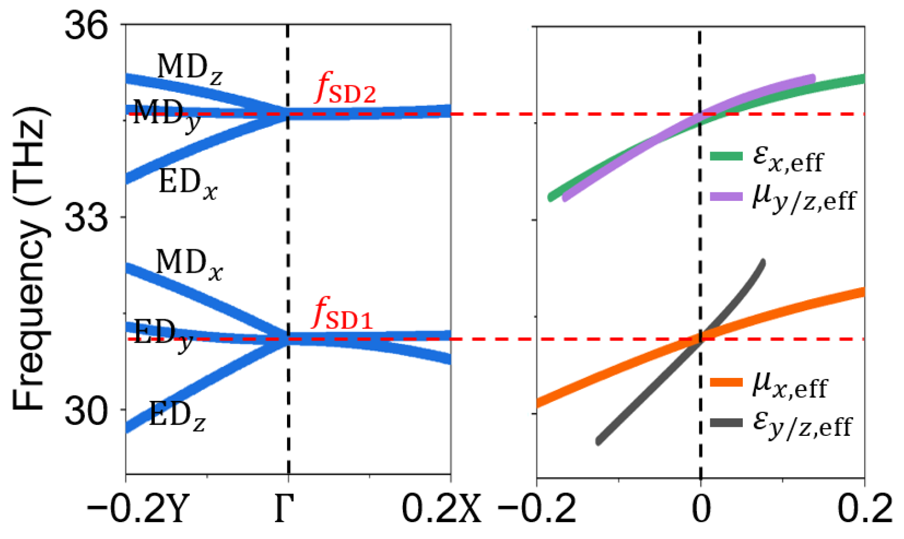
3. PhC-Based Effective AZIM

Next, we demonstrate that the silicon PhC featuring dual semi-Dirac cones can function as an effective AZIM operating at two distinct frequencies. For the transverse modes in the vicinity of the Γ point, the silicon PhC can be homogenized as a uniform medium, characterized by an effective relative permittivity tensor ε ̿ e f f = ε x , e f f 0 0 0 ε y , e f f 0 0 0 ε z , e f f and an effective relative permeability tensor μ ̿ e f f = μ x , e f f 0 0 0 μ y , e f f 0 0 0 μ z , e f f , where ε y , e f f = ε z , e f f and μ y , e f f = μ z , e f f due to the structural symmetry.
The effective parameters of the PhC can be retrieved by matching the dispersion relations and surface impedances of the corresponding modes [66,69,70]. From the E D z and M D x modes along the Γ Y direction near the first semi-Dirac cone, the effective parameters ε z , e f f (or ε y , e f f ) and μ x , e f f can be determined using:
ε z , e f f = k y Z e f f 1 ε 0 ω = ε y , e f f μ x , e f f = k y Z e f f 1 μ 0 ω
where ε 0 and μ 0 are the permittivity and permeability of free space, respectively; ω is the angular frequency; k y is the y -component of Bloch wave vector; Z e f f 1 = E z / H x is the effective wave impedance for the E D z and M D x modes. The bracket denotes the average of eigenfields on the x z surface of the PhC unit cell. Similarly, in the vicinity of the second semi-Dirac cone, based on the E D x and M D z modes along the Γ Y direction, the effective parameters ε x , e f f and μ z , e f f (or μ y , e f f ) can be obtained using:
ε x , e f f = k y Z e f f 2 ε 0 ω μ z , e f f = k y Z e f f 2 μ 0 ω = μ y , e f f ,
where Z e f f 2 = E x / H z is the effective wave impedance for the E D x and M D z modes.
The obtained effective parameters of the silicon PhC based on Equations (1) and (2) are plotted in the right panel of Figure 3. At the first semi-Dirac-point frequency f S D 1 , we have ε y , e f f = ε z , e f f = μ x , e f f = 0 . This indicates that the PhC behaves as an effective double-zero material with both effective permittivity and permeability approaching zero for the y and z propagation directions. A material with double-zero parameters can be considered an electromagnetic void space, with electromagnetic properties equivalent to those of a vacuum point, according to the transformation optics [24]. Consequently, such a double-zero material allows for perfect transmission with no phase accumulation. Additionally, based on the transfer matrix method, it can be demonstrated that the transfer matrix for the double-zero material under normal incidence is a unity matrix, which corresponds perfect transmission [46]. In contrast, for the x propagation direction, the PhC acts as a single-zero material with only effective permittivity approaching zero, indicating extreme impedance mismatch with free space and a pronounced wave-blocking effect [46].
Simultaneously, at the second semi-Dirac-point frequency f S D s , the PhC functions as an effective double-zero material that is wave transparent for waves of the y and z propagation directions, while an impedance-mismatched single-zero material (only the effective permeability is near-zero) with a wave-blocking effect for the x propagation direction. Clearly, highly anisotropic wave transport properties due to the extreme anisotropy are expected within the PhC-based AZIM, as discussed in detail in the following section.

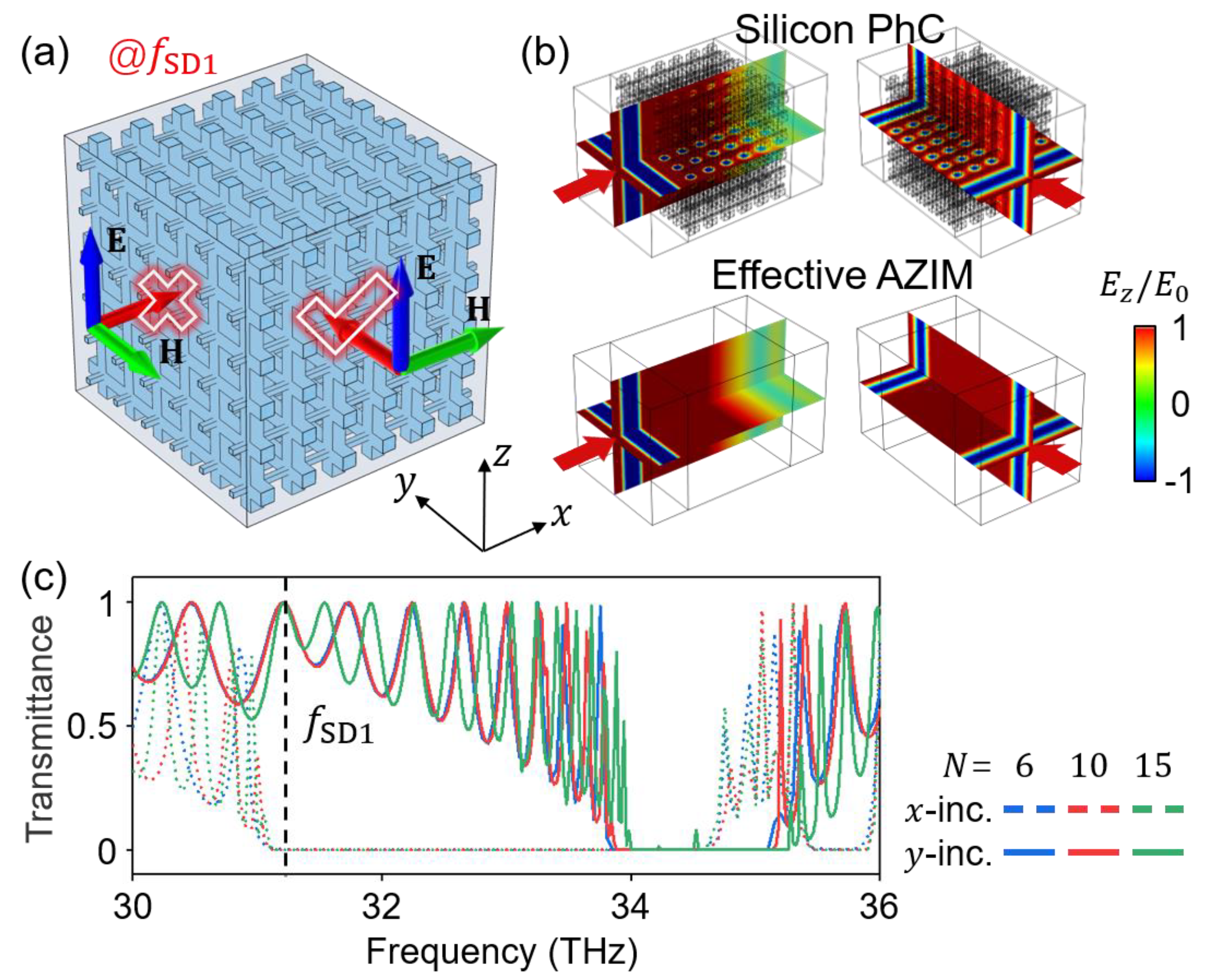
4. Highly Anisotropic Wave Transport Property

To demonstrate the highly anisotropic wave transport properties within the PhC-based AZIM, we investigated a silicon PhC cube composed of N × N × N unit cells under the illumination of waves propagating in different directions at the two semi-Dirac-point frequencies f S D 1 and f S D 2 .
We first examined the wave transmission behaviors at the first semi-Dirac-point frequency f S D 1 . Here, normal incidence is emphasized to prevent the excitation of longitudinal modes within the flat band. The wave vector is assumed to be along either the x or y direction, with the electric field polarized along the z direction. Figure 4a illustrates the anisotropic wave transport behavior of the PhC-based AZIM. According to the effective-medium description in Figure 3, the PhC-based AZIM is expected to exhibit near-perfect transmission for y -incidence (i.e., wave vector along the y direction), as the incident wave “sees” double-zero effective parameters, specifically, ε z , e f f = 0 and μ x , e f f = 0 . Conversely, for x -incidence (i.e., wave vector along the x direction), the PhC-based AZIM demonstrates a wave-blocking effect due to extreme impedance mismatch with free space, as it behaves as a single-zero material with ε z , e f f = 0 and μ y , e f f 0 at f S D 1 .
The numerical verification is presented in Figure 4b, where the distributions of a normalized electric field E z / E 0 ( E 0 is the electric field amplitude of incidence) are plotted for the silicon PhC cube consisting of 6 × 6 × 6 unit cells (upper) and its corresponding effective AZIM (lower), for x -incidence (left) and y -incidence (right) at f S D 1 = 31.12   T H z . The results from the PhC model and the effective medium model agree well, both showing a strong wave-blocking effect for x -incidence and near-perfect wave-transparency for y -incidence, consistent with theoretical expectations. Furthermore, the transmittance through a silicon PhC cube composed of N × N × N unit cells ( N = 6 , 10 , 15 ) as a function of working frequency is plotted for x -incidence (dashed lines) and y -incidence (solid lines). For y -incidence, a series of transmission peaks are observed. Almost all of them are induced by Fabry–Pérot resonances within the PhC cube, and therefore, they are N -dependent, except for the transmission peak at f S D 1 = 31.12   T H z . The unique transmission peak at f S D 1 = 31.12   T H z is N -independent, suggesting it results from the double-zero characteristic of the PhC-based AZIM. Conversely, at the same frequency, the transmission for x -incidence is quite low, as the result of the impedance-mismatched single-zero property. Furthermore, it is noted that the PhC cube exhibits a pronounced wave-blocking effect for x-incidence within the frequency range of f S D 1 f S D 2 , due to the presence of a directional band gap along the Γ X direction within this range, as observed from the band structure in Figure 2b. These results demonstrate the pronounced anisotropic wave transport property within the PhC-based AZIM at the semi-Dirac-point frequency f S D 1 .
A similar anisotropic wave transport property is observed at the second semi-Dirac-point frequency f S D 2 , but with a different polarization. As depicted in Figure 5a, for waves with the magnetic field polarized along the z direction, the PhC-based AZIM exhibits near-perfect transparency for y -incidence, while showing a strong wave-blocking effect for x -incidence. This anisotropic behavior is confirmed by the distributions of normalized magnetic field H z / H 0 ( H 0 is the magnetic-field amplitude of incidence) at f S D 2 = 34.60   T H z , as shown in Figure 5b. The upper and lower panels show the fields for the silicon PhC cube consisting of 6 × 6 × 6 unit cells and its corresponding effective AZIM, respectively. The left and right panels show the cases of x -incidence and y -incidence, respectively. The anisotropic wave transport property is further validated by the transmittance spectra presented in Figure 5c. At f S D 2 = 34.60   T H z , near-perfect transmission for y -incidence is observed, independent of the number of unit cells N , confirming the double-zero characteristic of the PhC-based AZIM. In contrast, low transmission (~0.13 for N = 6 ; ~0.12 for N = 10 ; ~0.11 for N = 15 ) for x -incidence is seen, consistent with the impedance-mismatched single-zero property. It is noted that the transmission for x -incidence at f S D 2 is relatively higher compared to that at f S D 1 , due to the limited number of unit cells N and the less pronounced impedance mismatch with free space, as inferred from the effective parameters in Figure 3. In fact, as the number of unit cells N increases, the transmission is expected to decrease for x -incidence at f S D 2 .
We note that the low transmission within the frequency range of f S D 1 f S D 2 for x-incidence is caused by the directional band gap along the Γ X direction. In contrast, for y -incidence, the PhC cube is wave-transparent over a broad frequency band. As shown by the effective parameters in Figure 3, ε x , e f f μ z , e f f across a wide frequency band, indicating that the effective impedance of the PhC is nearly matched with that of free space over this range. Consequently, N -independent near-perfect transmission is observed for y -incidence across a broad frequency band.
Overall, these results demonstrate that the silicon PhC, with dual semi-Dirac cones, effectively functions as a dual-band AZIM, exhibiting highly anisotropic wave transport properties across both frequencies for two distinct polarizations, paving the way for advanced wave and polarization control. Although ideal plane waves are assumed here, the designed PhC-based AZIM can also demonstrate its distinctive properties when illuminated by Gaussian beams with broad beam widths, provided that the PhC cube comprises a sufficient number of unit cells [65,66].

5. Discussion

It is noteworthy that the existing investigations on AZIMs utilizing dielectric PhCs with semi-Dirac cones predominantly focus on two-dimensional systems [60,61,62,63,64,65]. These two-dimensional configurations inherently lack the degrees of freedom, typically yielding only a single semi-Dirac cone per PhC and consequently restricting the operational bandwidth of the PhC-based AZIM. Moreover, the predetermined polarization states in two-dimensional systems significantly constrain their capabilities in wave manipulation [60,61,62,63,64,65]. Notably, our proposed three-dimensional silicon PhCs with dual semi-Dirac cones offer a promising platform for realizing low-loss dual-band AZIMs, enhancing functionalities in wave transport and polarization manipulation.
The key mechanism for achieving dual-band AZIMs lies in achieving accidental degeneracy of ED and MD modes at two distinct frequencies at the center of the Brillouin zone. Such mode degeneracies can give rise to Dirac-like cones or semi-Dirac cones, which are associated with zero effective permittivity and/or permeability. Although the present study and our previous work [66] are grounded in this concept, the design strategies differ significantly. In [66], core–shell particles are employed to modulate ED and MD modes in the guidance of the well-established Mie resonance theory, where the metallic core primarily governs the ED modes and the dielectric shell predominantly influences the MD modes. In contrast, the present work employs an approach based on crossed all-dielectric rods to simultaneously control both ED and MD modes. Although this strategy is usually more challenging, it offers the advantage of being free from material losses.
Considering only dipolar modes, we can achieve at most two semi-Dirac cones (or two AZIM operational frequencies). Although, in principle, employing higher-order modes (e.g., quadrupolar modes) at higher frequencies could increase the number of degeneracy points, the PhC dominated by these higher-order modes usually cannot be well regarded as an effective medium due to effects like lattice diffraction [71].

6. Conclusions

In summary, we have demonstrated a low-loss dual-band AZIM based on a three-dimensional terahertz silicon PhC exhibiting dual semi-Dirac cones at two distinct frequencies. At these frequencies, the PhC-based AZIM reveals highly anisotropic wave transport properties. It showcases near-perfect transmission for y (or z )-incidence due to the double-zero characteristic, and markedly low transmission for x -incidence attributed to the impedance-mismatched single-zero characteristic, for two distinct polarizations. The proposed PhC-based AZIM presents a viable approach for advanced wave transport and polarization manipulation, featuring an expanded operational bandwidth and ultra-low material losses.

Author Contributions

Conceptualization, J.L. and Y.L.; methodology, B.S.; software, B.S., R.M. and M.L.; validation, Y.X.; formal analysis, B.S.; investigation, B.S., R.M. and M.L.; resources, B.S., R.M. and M.L.; data curation, B.S., R.M. and M.L.; writing—original draft preparation, J.L. and B.S.; writing—review and editing, J.L., Y.L. and B.S.; visualization, R.M. and M.L.; supervision, J.L., Y.X. and Y.L.; project administration, J.L., Y.X. and Y.L.; funding acquisition, J.L., Y.X. and Y.L. All authors have read and agreed to the published version of the manuscript.

Funding

This research was funded by the National Natural Science Foundation of China (Grants No. 12374293, No. 11974010, and No. 12274313), the Natural Science Foundation of Jiangsu Province (Grant No. BK20221354).

Institutional Review Board Statement

Not applicable.

Informed Consent Statement

Not applicable.

Data Availability Statement

The data of this study are available from the corresponding author upon request.

Conflicts of Interest

The authors declare no conflicts of interest.

References

  1. Liberal, I.; Engheta, N. Near-zero refractive index photonics. Nat. Photonics 2017, 11, 149–158. [Google Scholar] [CrossRef]
  2. Niu, X.; Hu, X.; Chu, S.; Gong, Q. Epsilon-near-zero photonics: A new platform for integrated devices. Adv. Opt. Mater. 2018, 2018, 1701292. [Google Scholar] [CrossRef]
  3. Kinsey, N.; DeVault, C.; Boltasseva, A.; Shalaev, V.M. Near-zero-index materials for photonics. Nat. Rev. Mater. 2019, 4, 742–760. [Google Scholar] [CrossRef]
  4. Vertchenko, L.; Nikitin, M.; Lavrinenko, A. Near-zero-index platform in photonics: Tutorial. J. Opt. Soc. Am. B 2023, 40, 1467. [Google Scholar] [CrossRef]
  5. Silveirinha, M.; Engheta, N. Tunneling of electromagnetic energy through subwavelength channels and bends using ϵ-near-zero materials. Phys. Rev. Lett. 2006, 97, 157403. [Google Scholar] [CrossRef]
  6. Edwards, B.; Alù, A.; Young, M.; Silveirinha, M.; Engheta, N. Experimental verification of epsilon-near-zero metamaterial coupling and energy squeezing using a microwave waveguide. Phys. Rev. Lett. 2008, 100, 33903. [Google Scholar] [CrossRef]
  7. Liu, R.; Cheng, Q.; Hand, T.; Mock, J.; Cui, T.; Cummer, S.; Smith, D. Experimental demonstration of electromagnetic tunneling through an epsilon-near-zero metamaterial at microwave frequencies. Phys. Rev. Lett. 2008, 100, 23903. [Google Scholar] [CrossRef]
  8. Yan, W.; Zhou, Z.; Li, H.; Li, Y. Transmission-type photonic doping for high-efficiency epsilon-near-zero supercoupling. Nat. Commun. 2023, 14, 6154. [Google Scholar] [CrossRef]
  9. Ma, H.F.; Shi, J.H.; Jiang, W.X.; Cui, T.J. Experimental realization of bending waveguide using anisotropic zero-index materials. Appl. Phys. Lett. 2012, 101, 253513. [Google Scholar] [CrossRef]
  10. Enoch, S.; Tayeb, G.; Sabouroux, P.; Guérin, N.; Vincent, P. A metamaterial for directive emission. Phys. Rev. Lett. 2002, 89, 213902. [Google Scholar] [CrossRef]
  11. Cheng, Q.; Jiang, W.X.; Cui, T.J. Spatial power combination for omnidirectional radiation via anisotropic metamaterials. Phys. Rev. Lett. 2012, 108, 213903. [Google Scholar] [CrossRef] [PubMed]
  12. Luo, J.; Lu, W.; Hang, Z.; Chen, H.; Hou, B.; Lai, Y.; Chan, C.T. Arbitrary control of electromagnetic flux in inhomogeneous anisotropic media with near-zero index. Phys. Rev. Lett. 2014, 112, 73903. [Google Scholar] [CrossRef]
  13. Ji, W.; Luo, J.; Lai, Y. Extremely anisotropic epsilon-near-zero media in waveguide metamaterials. Opt. Express 2019, 27, 19463–19473. [Google Scholar] [CrossRef] [PubMed]
  14. Mei, R.; Xu, Y.; Gao, L.; Xu, H.X.; Lai, Y.; Luo, J. Skin effect of electromagnetic flux in anisotropic zero-index metamaterials. Adv. Opt. Mater. 2024, 2024, 2401569. [Google Scholar] [CrossRef]
  15. Liberal, I.; Mahmoud, A.M.; Li, Y.; Edwards, B.; Engheta, N. Photonic doping of epsilon-near-zero media. Science 2017, 355, 1058–1062. [Google Scholar] [CrossRef] [PubMed]
  16. Liberal, I.; Li, Y.; Engheta, N. Reconfigurable epsilon-near-zero metasurfaces via photonic doping. Nanophotonics 2018, 7, 1117–1127. [Google Scholar] [CrossRef]
  17. Luo, J.; Li, J.; Lai, Y. Electromagnetic impurity-immunity induced by parity-time symmetry. Phys. Rev. X 2018, 8, 31035. [Google Scholar] [CrossRef]
  18. Luo, J.; Liu, B.; Hang, Z.H.; Lai, Y. Coherent perfect absorption via photonic doping of zero-index media. Laser Photonics Rev. 2018, 2018, 1800001. [Google Scholar] [CrossRef]
  19. Zhou, Z.; Li, Y.; Li, H.; Sun, W.; Liberal, I.; Engheta, N. Substrate-integrated photonic doping for near-zero-index devices. Nat. Commun. 2019, 10, 4132. [Google Scholar] [CrossRef]
  20. Coppolaro, M.; Moccia, M.; Castaldi, G.; Engheta, N.; Galdi, V. Non-Hermitian doping of epsilon-near-zero media. Proc. Natl. Acad. Sci. USA 2020, 117, 13921–13928. [Google Scholar] [CrossRef]
  21. Zhou, Q.; Fu, Y.; Huang, L.; Wu, Q.; Miroshnichenko, A.; Gao, L.; Xu, Y. Geometry symmetry-free and higher-order optical bound states in the continuum. Nat. Commun. 2021, 12, 4390. [Google Scholar] [CrossRef] [PubMed]
  22. Li, H.; Fu, P.; Zhou, Z.; Sun, W.; Li, Y.; Wu, J.; Dai, Q. Performing calculus with epsilon-near-zero metamaterials. Sci. Adv. 2022, 8, eabq6198. [Google Scholar] [CrossRef] [PubMed]
  23. Xu, C.; Chu, H.; Luo, J.; Hang, Z.H.; Wu, Y.; Lai, Y. Three-dimensional electromagnetic void space. Phys. Rev. Lett. 2021, 127, 123902. [Google Scholar] [CrossRef] [PubMed]
  24. Yan, D.; Mei, R.; Li, M.; Ma, Z.; Hang, Z.H.; Luo, J. Controlling coherent perfect absorption via long-range connectivity of defects in three-dimensional zero-index media. Nanophotonics 2023, 12, 4205–4214. [Google Scholar] [CrossRef]
  25. Liu, C.; Yan, D.; Sun, B.; Xu, Y.; Fang, C.; Gao, L.; Luo, J. Low-gain generalized pt symmetry for electromagnetic impurity-immunity via non-Hermitian doped zero-index materials. Photonics Res. 2024, 12, 2424–2434. [Google Scholar] [CrossRef]
  26. Alam, M.Z.; De Leon, I.; Boyd, R.W. Large optical nonlinearity of indium tin oxide in its epsilon-near-zero region. Science 2016, 352, 795–797. [Google Scholar] [CrossRef]
  27. Alam, M.Z.; Schulz, S.A.; Upham, J.; De Leon, I.; Boyd, R.W. Large optical nonlinearity of nanoantennas coupled to an epsilon-near-zero material. Nat. Photonics 2018, 12, 79–83. [Google Scholar] [CrossRef]
  28. Yang, Y.; Lu, J.; Manjavacas, A.; Luk, T.S.; Liu, H.; Kelley, K.; Maria, J.; Runnerstrom, E.L.; Sinclair, M.B.; Ghimire, S.; et al. High-harmonic generation from an epsilon-near-zero material. Nat. Phys. 2019, 15, 1022–1026. [Google Scholar] [CrossRef]
  29. Caspani, L.; Kaipurath, R.P.M.; Clerici, M.; Ferrera, M.; Roger, T.; Kim, J.; Kinsey, N.; Pietrzyk, M.; Di Falco, A.; Shalaev, V.M.; et al. Enhanced nonlinear refractive index in ε-near-zero materials. Phys. Rev. Lett. 2016, 116, 233901. [Google Scholar] [CrossRef]
  30. Jia, W.; Liu, M.; Lu, Y.; Feng, X.; Wang, Q.; Zhang, X.; Ni, Y.; Hu, F.; Gong, M.; Xu, X.; et al. Broadband terahertz wave generation from an epsilon-near-zero material. Light-Sci. Appl. 2021, 10, 11. [Google Scholar] [CrossRef]
  31. Reshef, O.; De Leon, I.; Alam, M.Z.; Boyd, R.W. Nonlinear optical effects in epsilon-near-zero media. Nat. Rev. Mater. 2019, 4, 535–551. [Google Scholar] [CrossRef]
  32. Vertchenko, L.; Lavrinenko, A. Implications of Low-Refractive Mode Index on Nonlinear Optical Interactions. Laser Photonics Rev. 2023, 17, 2200741. [Google Scholar] [CrossRef]
  33. Wang, C.; Shi, R.; Gao, L.; Shalin, A.S.; Luo, J. Quenching of second-harmonic generation by epsilon-near-zero media. Photonics Res. 2023, 11, 1437. [Google Scholar] [CrossRef]
  34. Lobet, M.; Liberal, I.; Vertchenko, L.; Lavrinenko, A.V.; Engheta, N.; Mazur, E. Momentum considerations inside near-zero index materials. Light-Sci. Appl. 2022, 11, 110. [Google Scholar] [CrossRef] [PubMed]
  35. Adams, D.C.; Inampudi, S.; Ribaudo, T.; Slocum, D.; Vangala, S.; Kuhta, N.A.; Goodhue, W.D.; Podolskiy, V.A.; Wasserman, D. Funneling light through a subwavelength aperture with epsilon-near-zero materials. Phys. Rev. Lett. 2011, 107, 133901. [Google Scholar] [CrossRef] [PubMed]
  36. Kim, J.; Dutta, A.; Naik, G.V.; Giles, A.J.; Bezares, F.J.; Ellis, C.T.; Tischler, J.G.; Mahmoud, A.M.; Caglayan, H.; Glembocki, O.J. Role of epsilon-near-zero substrates in the optical response of plasmonic antennas. Optica 2016, 3, 339–346. [Google Scholar] [CrossRef]
  37. Xu, J.; Mandal, J.; Raman, A.P. Broadband directional control of thermal emission. Science 2021, 372, 393–397. [Google Scholar] [CrossRef]
  38. Wu, J.; Clementi, M.; Huang, C.; Ye, F.; Fu, H.; Lu, L.; Zhang, S.; Li, Q.; Bres, C.S. Thermo-optic epsilon-near-zero effects. Nat. Commun. 2024, 15, 794. [Google Scholar] [CrossRef]
  39. Anopchenko, A.; Gurung, S.; Tao, L.; Arndt, C.; Lee, H.W.H. Atomic layer deposition of ultra-thin and smooth Al-doped ZnO for zero-index photonics. Mater. Res. Express 2018, 5, 14012. [Google Scholar] [CrossRef]
  40. Tao, L.; Anopchenko, A.; Gurung, S.; Zhang, J.; Lee, H.W.H. Gate-tunable plasmon-induced transparency modulator based on stub-resonator waveguide with epsilon-near-zero materials. Sci. Rep. 2019, 9, 2789. [Google Scholar] [CrossRef]
  41. Lee, H.W.; Papadakis, G.; Burgos, S.P.; Chander, K.; Kriesch, A.; Pala, R.; Peschel, U.; Atwater, H.A. Nanoscale conducting oxide plasMOStor. Nano Lett. 2014, 14, 6463–6468. [Google Scholar] [CrossRef]
  42. Anopchenko, A.; Gurung, S.; Bej, S.; Lee, H.W.H. Field enhancement of epsilon-near-zero modes in realistic ultrathin absorbing films. Nanophotonics 2023, 12, 2913–2920. [Google Scholar] [CrossRef]
  43. Zhang, L.; Love, S.; Anopchenko, A.; Lee, H.W.H. Hollow core optical fiber enabled by epsilon-near-zero material. Nanophotonics 2024, 13, 1025–1031. [Google Scholar] [CrossRef]
  44. Maas, R.; Parsons, J.; Engheta, N.; Polman, A. Experimental realization of an epsilon-near-zero metamaterial at visible wavelengths. Nat. Photonics 2013, 7, 907–912. [Google Scholar] [CrossRef]
  45. Dai, J.; Jiang, H.; Guo, Z.; Qiu, J. Tunable epsilon-and-mu-near-zero metacomposites. Adv. Funct. Mater. 2023, 34, 2308338. [Google Scholar] [CrossRef]
  46. Luo, J.; Lai, Y. Epsilon-near-zero or mu-near-zero materials composed of dielectric photonic crystals. Sci. China Inf. Sci. 2013, 56, 1–10. [Google Scholar] [CrossRef]
  47. Qin, X.; Sun, W.; Zhou, Z.; Fu, P.; Li, H.; Li, Y. Waveguide effective plasmonics with structure dispersion. Nanophotonics 2022, 11, 1659–1676. [Google Scholar] [CrossRef]
  48. Ji, W.; Luo, J.; Chu, H.; Zhou, X.; Meng, X.; Peng, R.; Wang, M.; Lai, Y. Crosstalk prohibition at the deep-subwavelength scale by epsilon-near-zero claddings. Nanophotonics 2023, 12, 2007–2017. [Google Scholar] [CrossRef]
  49. Vulis, D.I.; Reshef, O.; Camayd-Muñoz, P.; Mazur, E. Manipulating the flow of light using Dirac-cone zero-index metamaterials. Rep. Prog. Phys. 2019, 82, 12001. [Google Scholar] [CrossRef]
  50. Li, Y.; Chan, C.T.; Mazur, E. Dirac-like cone-based electromagnetic zero-index metamaterials. Light-Sci. Appl. 2021, 10, 203. [Google Scholar] [CrossRef]
  51. Luo, J.; Lai, Y. Hermitian and non-Hermitian Dirac-like cones in photonic and phononic structures. Front. Phys. 2022, 10, 845624. [Google Scholar] [CrossRef]
  52. Huang, X.; Lai, Y.; Hang, Z.H.; Zheng, H.; Chan, C.T. Dirac cones induced by accidental degeneracy in photonic crystals and zero-refractive-index materials. Nat. Mater. 2011, 10, 582–586. [Google Scholar] [CrossRef]
  53. Moitra, P.; Yang, Y.; Anderson, Z.; Kravchenko, I.I.; Briggs, D.P.; Valentine, J. Realization of an all-dielectric zero-index optical metamaterial. Nat. Photonics 2013, 7, 791–795. [Google Scholar] [CrossRef]
  54. Li, Y.; Kita, S.; Muñoz, P.; Reshef, O.; Vulis, D.I.; Yin, M.; Lončar, M.; Mazur, E. On-chip zero-index metamaterials. Nat. Photonics 2015, 9, 738–742. [Google Scholar] [CrossRef]
  55. Dong, T.; Dai, T.; Chen, Y.; Liu, Y.; Liu, H.; Wang, Y.; Ma, A.; Hu, H.; Xu, L.; Zhao, L.; et al. Low-loss nanoscale zero-index metawaveguides and metadevices. Optica 2024, 11, 799. [Google Scholar] [CrossRef]
  56. Tang, H.; DeVault, C.; Camayd-Muñoz, S.A.; Liu, Y.; Jia, D.; Du, F.; Mello, O.; Vulis, D.I.; Li, Y.; Mazur, E. Low-loss zero-index materials. Nano Lett. 2021, 21, 914–920. [Google Scholar] [CrossRef]
  57. Dong, T.; Liang, J.; Camayd-Muñoz, S.; Liu, Y.; Tang, H.; Kita, S.; Chen, P.; Wu, X.; Chu, W.; Mazur, E.; et al. Ultra-low-loss on-chip zero-index materials. Light-Sci. Appl. 2021, 10, 10. [Google Scholar] [CrossRef]
  58. Liu, Y.; Dong, T.; Qin, X.; Luo, W.; Leng, N.; He, Y.; Yuan, Y.; Bai, M.; Sun, J.; Zhou, J.; et al. High-permittivity ceramics enabled highly homogeneous zero-index metamaterials for high-directivity antennas and beyond. Elight 2024, 4, 4. [Google Scholar] [CrossRef]
  59. Li, Y.; Mei, J. Double Dirac cones in two-dimensional dielectric photonic crystals. Opt. Express 2015, 23, 12089. [Google Scholar] [CrossRef]
  60. Wu, Y. A semi-Dirac point and an electromagnetic topological transition in a dielectric photonic crystal. Opt. Express 2014, 22, 1906–1917. [Google Scholar] [CrossRef]
  61. Yasa, U.G.; Turduev, M.; Giden, I.H.; Kurt, H. Full utilization of semi-Dirac cones in photonics. Phys. Rev. B 2018, 97, 195131. [Google Scholar] [CrossRef]
  62. Bor, E.; Turduev, M.; Yasa, U.G.; Kurt, H.; Staliunas, K. Asymmetric light transmission effect based on an evolutionary optimized semi-Dirac cone dispersion photonic structure. Phys. Rev. B 2018, 98, 245112. [Google Scholar] [CrossRef]
  63. Bor, E.; Gorkem Yasa, U.; Kurt, H.; Turduev, M. Demonstration of carpet cloaking by an anisotropic zero refractive index medium. Opt. Lett. 2020, 45, 2423. [Google Scholar] [CrossRef]
  64. Vertchenko, L.; DeVault, C.; Malureanu, R.; Mazur, E.; Lavrinenko, A. Near-zero index photonic crystals with directive bound states in the continuum. Laser Photonics Rev. 2021, 15, 2000559. [Google Scholar] [CrossRef]
  65. Yang, D.; Feng, F.; Sun, L.; Wang, N.; Wang, G.P. Realization of magneto-optical near-zero-index metamaterial by using an array of spinning cylinders. Phys. Rev. A 2022, 105, 43517. [Google Scholar] [CrossRef]
  66. Li, M.; Mei, R.; Yan, D.; Ma, Z.; Cao, F.; Xu, Y.; Xu, C.; Luo, J. Dual semi-Dirac cones in three-dimensional photonic crystals. Phys. Rev. B 2024, 109, 125432. [Google Scholar] [CrossRef]
  67. Shkondin, E.; Takayama, O.; Panah, M.E.A.; Liu, P.; Larsen, P.V.; Mar, M.D.; Jensen, F.; Lavrinenko, A.V. Large-scale high aspect ratio Al-doped ZnO nanopillars arrays as anisotropic metamaterials. Opt. Mater. Express 2017, 7, 1606. [Google Scholar] [CrossRef]
  68. van de Haar, M.A.; van de Groep, J.; Brenny, B.J.M.; Polman, A. Controlling magnetic and electric dipole modes in hollow silicon nanocylinders. Opt. Express 2016, 24, 2047–2064. [Google Scholar] [CrossRef]
  69. Luo, J.; Yang, Y.; Yao, Z.; Lu, W.; Hou, B.; Hang, Z.H.; Chan, C.T.; Lai, Y. Ultratransparent media and transformation optics with shifted spatial dispersions. Phys. Rev. Lett. 2016, 117, 223901. [Google Scholar] [CrossRef]
  70. Luo, H.; Luo, J.; Zhang, Z.; Wu, C.; Li, Q.; Liu, W.; Peng, R.; Wang, M.; Li, H.; Lai, Y. Dielectric metamaterials with effective self-duality and full-polarization omnidirectional brewster effect. Light-Sci. Appl. 2024, 13, 262. [Google Scholar] [CrossRef]
  71. Śmigaj, W.; Gralak, B. Validity of the effective-medium approximation of photonic crystals. Phys. Rev. B 2008, 77, 235445. [Google Scholar] [CrossRef]
Figure 1. (a) Schematic graph of a three-dimensional silicon PhC consisting of orthogonally aligned silicon rods. (b) The silicon PhC is designed to exhibit dual semi-Dirac cones, which can be effectively homogenized as a low-loss dual-band AZIM.
Photonics 11 01018 g001
Figure 2. (a) Schematic graph of the silicon PhC unit cell. (b) Photonic band structure of the PhC. (c) A zoomed-in view of the dual semi-Dirac conical dispersion (left), and electric-field distributions for the degenerate modes along the Γ Y direction as the frequency gradually increases near the semi-Dirac cones (right).
Photonics 11 01018 g002
Figure 3. A zoomed-in view of the dual semi-Dirac conical dispersion (left), and the effective parameters of the silicon PhC corresponding to the transverse modes (right).
Photonics 11 01018 g003
Figure 4. (a) Schematic graph of a silicon PhC cube that blocks waves for x -incidence, while is wave-transparent for y -incidence at the first semi-Dirac-point frequency f S D 1 . (b) Normalized electric field E z / E 0 for a silicon PhC cube consisting of 6 × 6 × 6 unit cells (upper) and its corresponding effective AZIM (lower) for the x -incidence (left) and y -incidence (right) at f S D 1 = 31.12   T H z . The electric field of incidence is polarized along the z direction. (c) Computed transmittance through a silicon PhC cube consisting of N × N × N unit cells ( N = 6 , 10 , 15 ) for x -incidence (dashed lines) and y -incidence (solid lines) as the function of working frequency.
Photonics 11 01018 g004
Figure 5. (a) Schematic graph of a silicon PhC cube that blocks waves for x -incidence, while is wave-transparent for y -incidence at the second semi-Dirac-point frequency f S D 2 . (b) Normalized magnetic field H z / H 0 for a silicon PhC cube consisting of 6 × 6 × 6 unit cells (upper) and its corresponding effective AZIM (lower) for the x -incidence (left) and y -incidence (right) at f S D 2 = 34.60   T H z . The magnetic field of incidence is polarized along the z direction. (c) Computed transmittance through a silicon PhC cube consisting of N × N × N unit cells ( N = 6 , 10 , 15 ) for x -incidence (dashed lines) and y -incidence (solid lines) as the function of working frequency.
Photonics 11 01018 g005
Disclaimer/Publisher’s Note: The statements, opinions and data contained in all publications are solely those of the individual author(s) and contributor(s) and not of MDPI and/or the editor(s). MDPI and/or the editor(s) disclaim responsibility for any injury to people or property resulting from any ideas, methods, instructions or products referred to in the content.

