Article

A CMOS Optoelectronic Transimpedance Amplifier Using Concurrent Automatic Gain Control for LiDAR Sensors

1
Division of Electronic and Semiconductor Engineering, Ewha Womans University, Seoul 03760, Republic of Korea
2
Graduate Program in Smart Factory, Ewha Womans University, Seoul 03760, Republic of Korea
*
Author to whom correspondence should be addressed.
These authors contributed equally to this work.
Photonics 2024, 11(10), 974; https://doi.org/10.3390/photonics11100974
Submission received: 6 August 2024 / Revised: 10 October 2024 / Accepted: 16 October 2024 / Published: 17 October 2024
(This article belongs to the Section Optoelectronics and Optical Materials)

Abstract

:
This paper presents a novel optoelectronic transimpedance amplifier (OTA) for short-range LiDAR sensors used in 180 nm CMOS technology, which consists of a main transimpedance amplifier (m-TIA) with an on-chip P+/N-well/Deep N-well avalanche photodiode (P+/NW/DNW APD) and a replica TIA with another on-chip APD, not only to acquire circuit symmetry but to also obtain concurrent automatic gain control (AGC) function within a narrow single pulse-width duration. In particular, for concurrent AGC operations, 3-bit PMOS switches with series resistors are added in parallel with the passive feedback resistor in the m-TIA. Then, the PMOS switches can be turned on or off in accordance with the DC output voltage amplitudes of the replica TIA. The post-layout simulations reveal that the OTA extends the dynamic range up to 74.8 dB (i.e., 1 µApp~5.5 mApp) and achieves a 67 dBΩ transimpedance gain, an 830 MHz bandwidth, a 16 pA/ Hz noise current spectral density, a −31 dBm optical sensitivity for a 10−12 bit error rate, and a 6 mW power dissipation from a single 1.8 V supply. The chip occupies a core area of 200 × 120 µm2.

1. Introduction

Light detection and ranging (LiDAR) technologies are widely utilized in various fields, including autonomous vehicles, robotics, indoor mapping, and home monitoring systems [1,2,3,4]. Especially in long-term care facilities for elders with senile dementia, it is crucial to have compact, low-power, and cost-effective sensors that can monitor elders in real time with no violation of their portrait rights and alert caregivers in urgent situations or emergencies, such as falls or abnormal movements. Owing to the global and rapid increase in the number of aging societies, the maintenance costs associated with protecting elderly individuals from injuries (i.e., falls) have been exponentially increasing [5]. LiDAR sensors are quite advantageous in these scenarios, as they can maintain privacy via blurred images while delivering accurate data on activities, like movement and even breathing rates. In addition, they are less affected by ambient RF interferences when compared to conventional RF-based sensors.
Typically, these systems are based on the pulsed time-of-flight (ToF) principle, which emits light pulses toward a target and captures the reflected signals to determine the distance based on the time interval between the transmitted and received pulses. Particularly for indoor applications such as home monitoring, these sensors’ effective range spans from a few centimeters to several meters, thus employing a dynamic range that can handle various signal intensities and ensure a quick response. However, a wider dynamic range allows for more precise detection and, hence, a novel receiver circuit design is mandatory to obtain these wide dynamic range characteristics.
For this purpose, automatic gain control (AGC) circuits have been frequently exploited in optical receivers, and various architectures of AGC mechanisms have been suggested [6,7,8,9,10,11]. Figure 1a shows a block diagram of a typical optical receiver, where the AGC loop consists of a variable-gain amplifier (VGA), an equalizer (EQ), an output buffer (OB), a peak detector, and an error amplifier. Therefore, the peak voltages of the output pulses are detected and amplified to control the gain of the VGA, extending the dynamic range. However, due to this long feedback loop, it is impossible to detect and control the amplitude of a single narrow pulse properly. Very often, the transimpedance amplifier (TIA) output signals must pass through a passive low-pass filter before connecting to the gain control switches, thus introducing a significant delay and, hence, failing to achieve single pulse detection.
Figure 1b presents a block diagram of the previously reported current-mode TIA with a single-pulse AGC function [11], where a mirrored current conveyor (MCC) input stage is inserted to monitor the incoming photocurrents, and the output voltages (IB_O) of the MCC stage are detected at the feedforward control-voltage generator (FCG) circuit. Then, the DC voltages of the FCG circuit are directly connected to the NMOS switches during the inverter transimpedance stage (INV-TIS) for gain control, thereby achieving AGC operations within a single pulse width. However, the MCC input stage includes five symmetric current-conveyor input buffers (SCC-IBs), giving rise to a large noise current spectral density, and thus deteriorating the optical sensitivity considerably.
In this paper, a novel TIA topology is proposed to overcome the aforementioned issues in the application of short-range LiDAR sensors. Here, a rather simpler and more cost-effective AGC mechanism is realized by exploiting dual on-chip CMOS avalanche photodiodes (APDs). Figure 2 presents a block diagram of the proposed optoelectronic transimpedance amplifier (OTA). It features a main transimpedance amplifier (m-TIA) with an on-chip APD and a replica TIA with another on-chip APD. The latter yields low DC voltages (VDC,AGC) to control the 3-bit PMOS switches in the m-TIA concurrently. Thereby, it reduces the transimpedance gain with respect to the amplitudes of the replica TIA output (Vout,r) during a narrow single pulse width (typ. 3~10 ns). The dual APDs are located very close to each other, and thus the optical pulses reflected from the target enter these two APDs simultaneously. Then, the output of the replica TIA becomes lower by the action of the cascaded common-source amplifiers (M7, M8), depending upon the incoming photocurrents. Hence, the AGC function can be conducted concurrently with the narrow input pulse signals.
This paper is organized as follows. Section 2 describes the operational principles of the proposed OTA in more detail. Section 3 provides the chip layout and post-layout simulation results. Then, the conclusion follows.

2. Circuit Description

TIAs are very crucial for analog front-end (AFE) receivers, as they determine the system’s overall performance. It is well known that conventional voltage-mode TIAs face limitations, such as a gain-bandwidth design tradeoff and a narrow input dynamic range, which might result in severe signal distortions, especially when large input photocurrents are entered. Although AGC circuits can be equipped in these voltage-mode TIAs, the signal recovery of a narrow LiDAR pulse is still very challenging. In addition, the delays introduced by feedback loops in traditional AGC mechanisms should be either avoided or reduced to enhance TIA performance; otherwise, this would lead to another challenge for circuit designs.

2.1. Proposed TIA with Concurrent AGC

In this work, we propose a novel AGC circuit that can eliminate the inevitable need for delayed feedback loops. Instead, the proposed ‘concurrent AGC’ circuit employs dual on-chip APDs at both input nodes of the m-TIA and the replica TIA, thereby enabling the control of the 3-bit PMOS switches in the m-TIA by the DC output voltages of the replica TIA, as described in Figure 2. This dual on-chip APD configuration helps the proposed OTA to not only achieve circuit symmetry, but also to guarantee a fast AGC function within a narrow single pulse width.
Figure 3 shows a schematic diagrams of an m-TIA equipped with the proposed concurrent AGC circuit and the replica TIA. Here, the m-TIA comprises an on-chip APD, a voltage-mode common-source amplifier (M1) with a feedback resistor array, and a PMOS transistor load (M2) with a cross-coupled NMOS source follower (M3 and RS). Therefore, the incoming optical pulses are converted into electrical currents (ipd) by the on-chip APD, and these signals are then fed into the m-TIA. Particularly, the cross-coupled NMOS source follower is exploited together with the PMOS load, hence enabling the output peak voltages to reach the supply voltage (VDD) [12]. Also, the feedback resistor array (RF and RFi(i=1~3)) is connected in parallel and operated by the PMOS switch transistors. For this purpose, the gate voltage (VC) is generated from the output of the replica TIA (M4~M6), followed by the cascaded common-source amplifiers (M7, M8) before entering the gates of the PMOS switches in the m-TIA. When substantial input currents enter the m-TIA, the VC increases and effectively adjusts the equivalent feedback resistance by varying the parallel combination of resistors. Namely, this mechanism enables AGC functioning by modulating the feedback resistance in response to the amplitudes of the input currents.

2.2. On-Chip APD

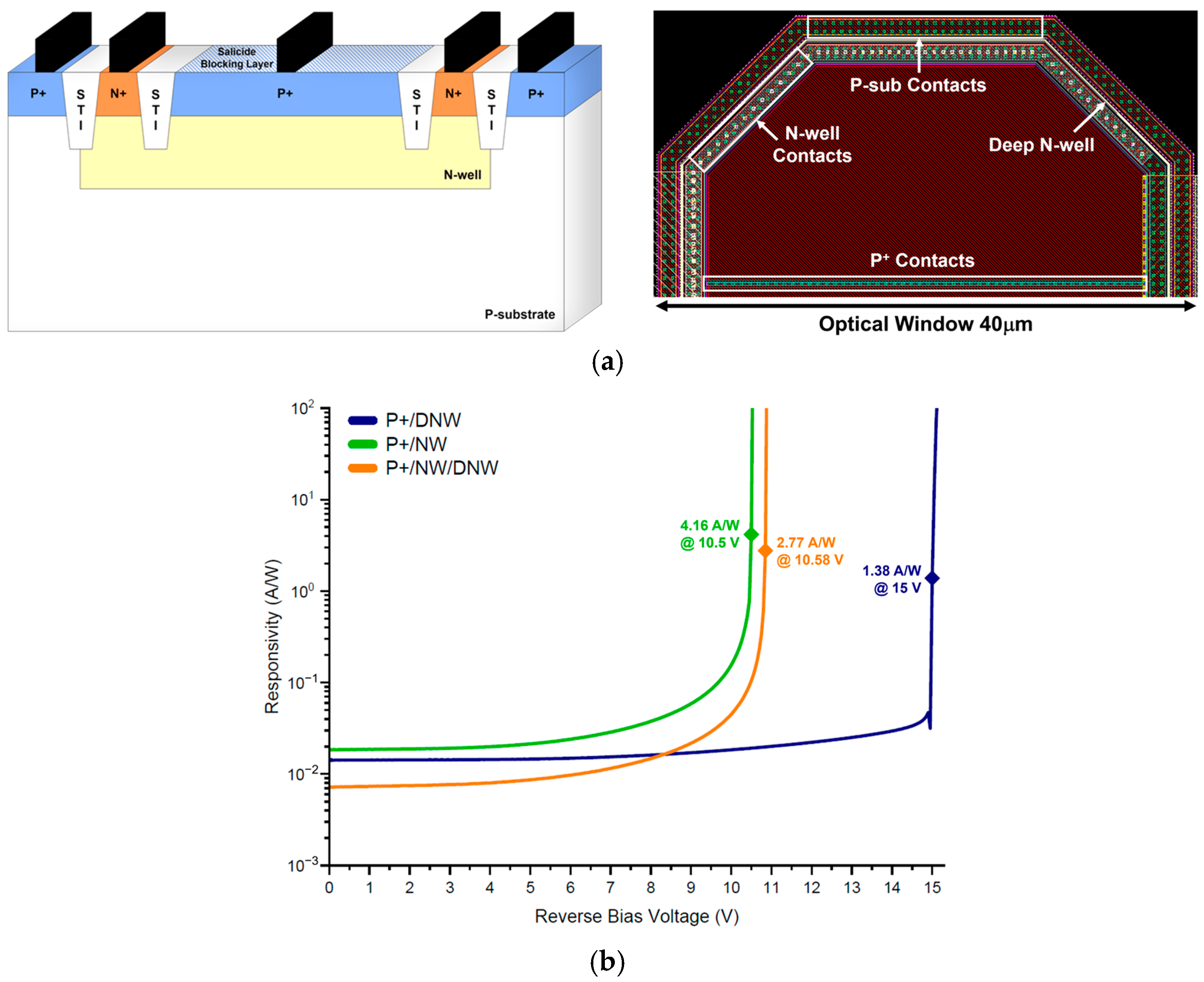
Optical receivers with off-chip photodetectors face significant challenges due to the signal distortions that occur from the variable bond-wire inductance. Also, the inevitable on-chip electrostatic discharge (ESD) protection diodes add to the parasitic capacitance, thereby shrinking the bandwidth considerably. Therefore, the on-chip integration of photodetectors helps to mitigate these issues, despite their deficient sensitivity in CMOS technologies, and also offers several advantages, including their compact size and low cost. Particularly, on-chip APDs are preferred to p-i-n photodiodes, even with their noisier characteristics, due to their ability to generate substantial photocurrents, which is suitable for short-range LiDAR sensor applications. Also, a P+/N-well/Deep N-well APD (P+/NW/DNW APD) architecture is incorporated into this work since it can be facilely optimized for better responsivity and a wider bandwidth than other topologies (typ. P+/NW APD). Figure 4a presents a cross-sectional view of the P+/NW/DNW APD, where avalanche multiplication is initiated by holes at the P+/NW junction, with shallow trench insulators (STIs) preventing premature edge breakdown. The incorporation of the DNW layer enhances the near-infrared sensitivity by reducing the number of holes penetrating into the p-substrate. In addition, the built-in potential barrier between the DNW and the p-substrate blocks the photocurrents generated in the p-substrate effectively, thus further improving the APD performance.
Figure 4b depicts an APD layout that adopts an octagonal shape to minimize the risk of edge breakdown. The P+ source and the drain regions are covered with a salicide blocking layer to form an optical window, hence ensuring that the high resistivity contacts remain exposed to reduce the contact resistivity [13]. The optical window, with a diagonal length of 40 µm, results in a total depletion capacitance (CPD) of 470 fF and a photodetection bandwidth of 1.7 GHz at a reverse bias of 10.25 V.

2.3. Tester Circuits: A2V and T2V Converters

In order to test the feasibility of the proposed OTA as the AFE circuit in short-range LiDAR sensors, the combination of analog-to-voltage (A2V) and time-to-voltage (T2V) converters is added to the OTA subsequently. These two converters can replace a complicated time-to-digital converter (TDC) circuit. The A2V converter can handle input currents up to 200 μApp, making it suitable for detecting signals reflected from targets located up to 10.2 m away, while the T2V converter takes on the TDC’s role in dealing with larger currents by converting the time interval between the emitted pulse and the reflected pulse into an output voltage. Then, the T2V converter can effectively accommodate a wider range of signal strengths, hence extending the minimum detection range to close to 30 cm.
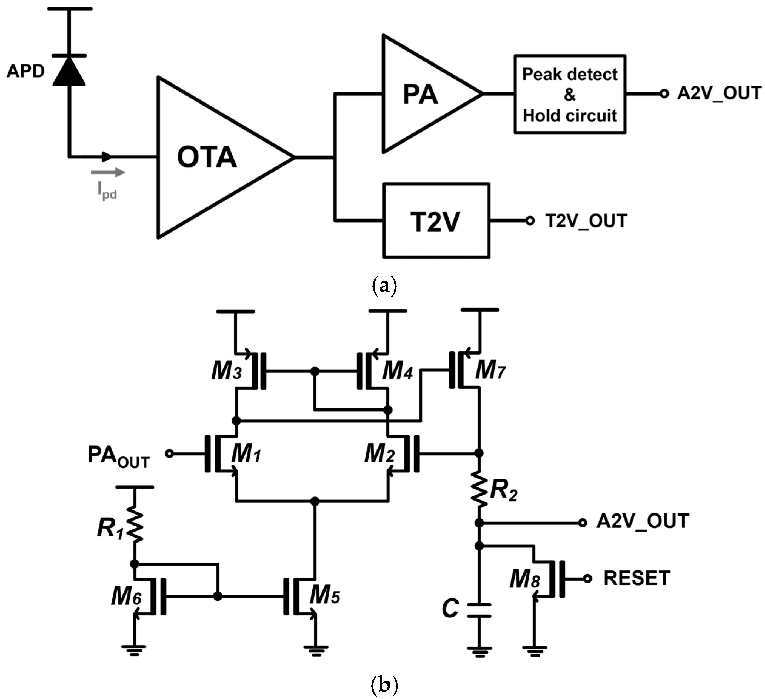
Figure 5a shows a block diagram of the tester circuit, where the A2V converter consists of a post-amplifier (PA) and a peak detect and hold (PDH) circuit. The voltage signals converted by the m-TIA are further amplified by the PA, and then the amplified signals enter the PDH circuit that can detect and maintain the peak voltages. The operation of the PDH circuit is divided into two phases, i.e., a write mode and a read mode. In the ‘write-mode’, the output voltage from the PA exceeds the reference voltage (A2V_OUT) and transistor M7 is turned on, thereby allowing the capacitor C to charge up to the voltage of PAOUT. As the PAOUT voltage begins to decrease from its peak, M7 is turned off and, therefore, the capacitor C retains the value of the peak voltage, thus transitioning the circuit into the ‘read-mode’. In this mode, the stored peak voltage can be read and utilized for further processing. The resistor R2 is introduced to enhance the stability of the PDH circuit, which creates a zero in the loop gain. This dual-mode operation ensures accurate peak voltage detection and retention, which is crucial for reliable signal processing in optical communication systems, such as LiDAR sensors.
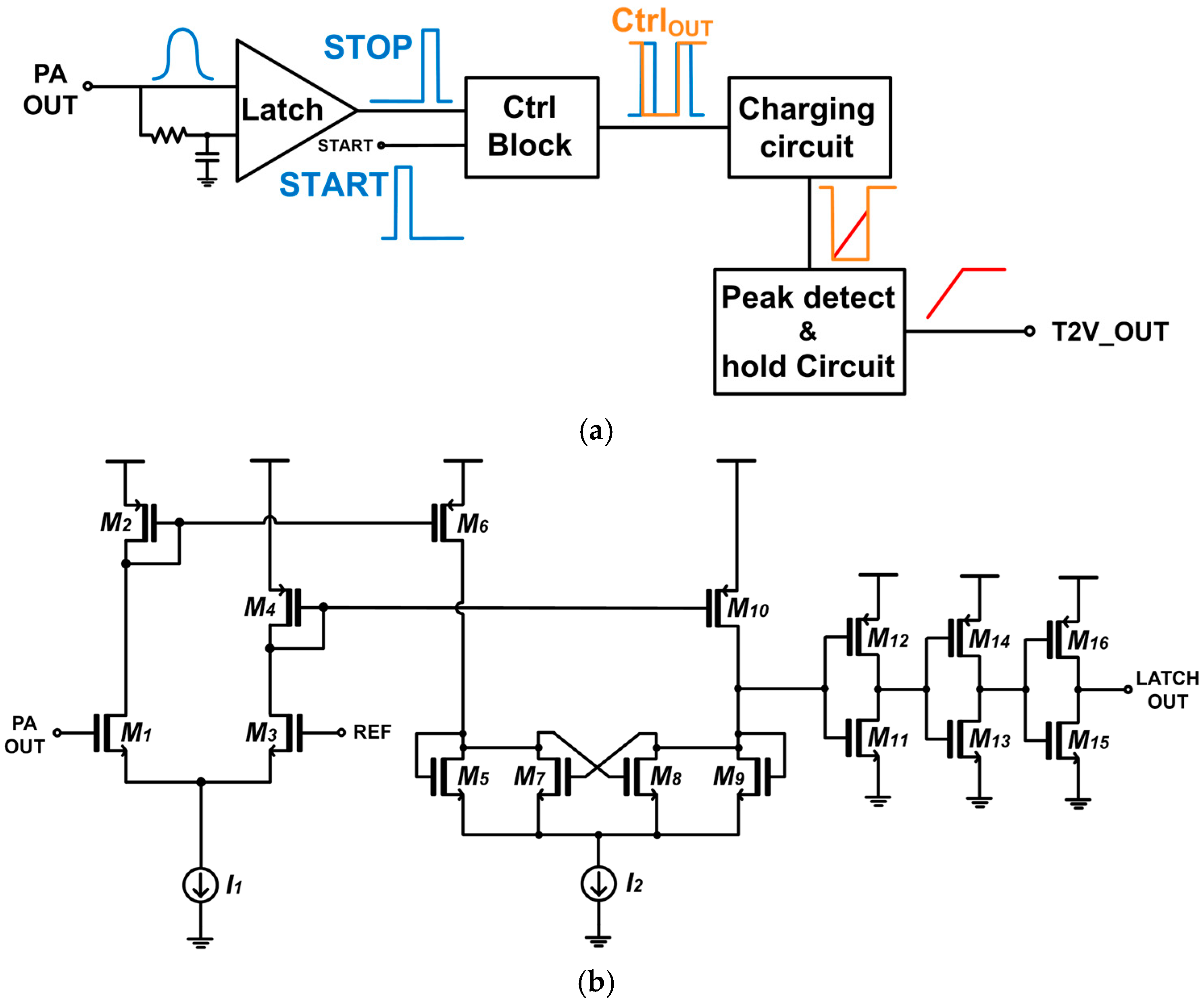
The T2V converter enhances the input dynamic range of the whole LiDAR receiver by converting the time-of-flight (ToF) information into their corresponding output voltages. It is particularly effective for measuring the reflection of light pulses from objects at varying distances. Figure 6a shows a block diagram of the T2V converter, which consists of a latch, a control block, a charging circuit, and a PDH circuit. In this T2V converter, the output signals from the PA are directly connected to the input latch comparator that converts the signals into digital pulses. Figure 6b presents a schematic diagram of the latch comparator. Specifically, the latch generates an output of ‘1’ if a pulse above the reference voltage is detected, and an output of ‘0’ otherwise. This latch output is fed into the control block along with the emitted signal (a.k.a. START) from the transmitter. This control block maintains an output of ‘0’ between the START and the receiving (a.k.a. STOP) of rising edges, when this output (CtrlOUT) drives the charging circuit to generate a triangular waveform. Upon detecting a latch output pulse (i.e., the rising edge of the STOP pulse), the control block switches the output to ‘1’. The duration between the START and STOP of the rising edges determines the rising time of the charging circuit, hence directly correlating it with the time-of-flight (ToF) information. Once the output from the control block returns to ‘1’, the charging circuit halts the voltage increment, thereby preserving the peak voltage. The charging circuit consists of an operational amplifier, a capacitor for charging through a load, and an NMOS transistor for reset functionality. Then, the output of this charging circuit is maintained by the PDH until the next reset signal arrives.
Meanwhile, the T2V converter ensures precise range detection by converting the ToF into a proportional voltage. Digital circuits, including the latch and control block, help mitigate notorious walk errors by generating accurate STOP pulses. Previously, various TDCs have been suggested to achieve precise time-interval measurements [14,15,16]. Yet, they mostly require complex algorithms. However, the proposed simple T2V converter provides a more simplified solution for accurate time-interval measurement, effectively replacing previous TDCs. In addition, the output levels can be mapped onto binary codes using a thermometer-to-binary circuit, which can then be used with an FPGA for further post-processing.

3. Chip Layout and Post-Layout Simulation Results

The post-layout simulations were performed by using the parameters of a standard 180 nm CMOS technology with the simulation software ‘Cadence 6.1.6 Spectre’. During these simulations, the on-chip APDs were modeled as equivalent electrical lumped elements, incorporating a series resistance of 25 Ω and a parasitic capacitance of 490 fF. Figure 7 shows the layout of the proposed LiDAR receiver, which includes two integrated on-chip P+/NW/DNW APDs and covers a core area of 200 × 120 μm2. The DC simulations reveal that the whole receiver dissipates 6 mW power consumption from a single 1.8 V supply.
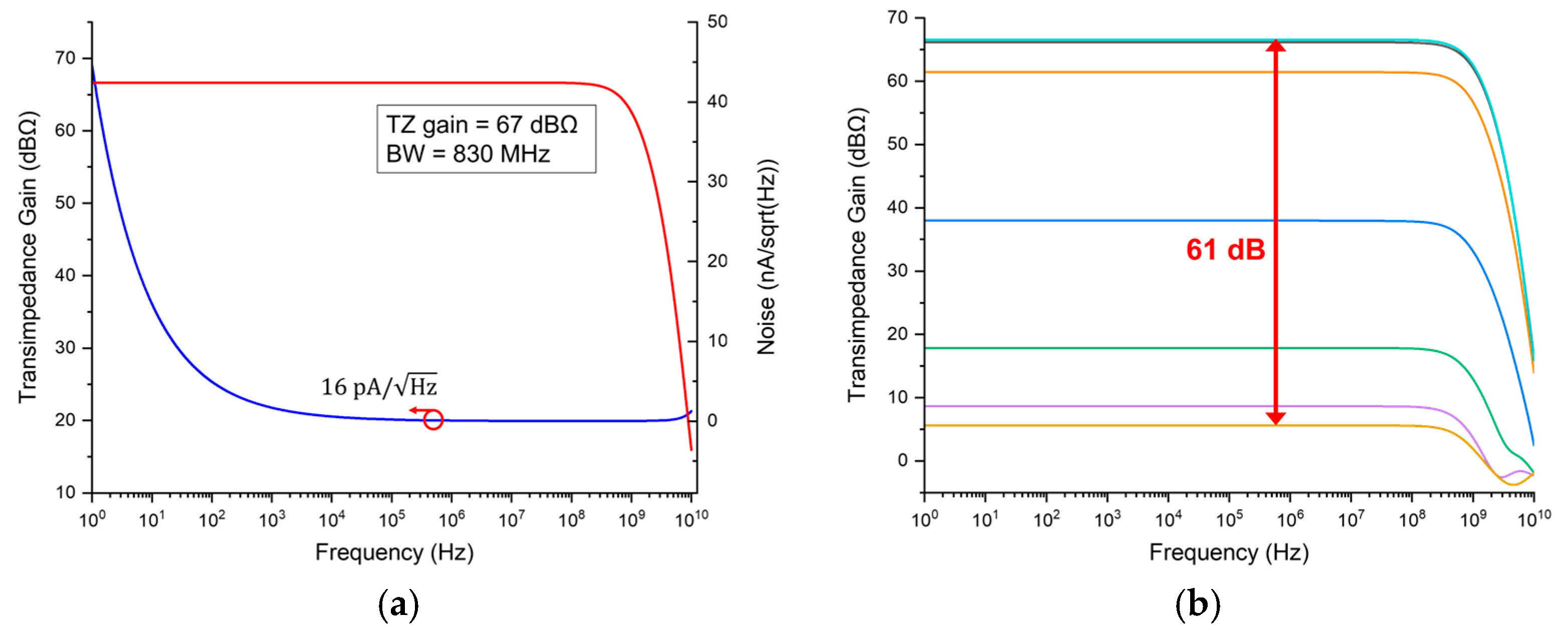
Figure 8a shows the simulated frequency responses of the proposed OTA, achieving a transimpedance gain of 67 dBΩ, a bandwidth of 830 MHz, and an average noise current spectral density of 16 pA / Hz that corresponds to an optical sensitivity of −31 dBm for a 10−12 bit error rate (BER), with the assumption of 4.16 A/W APD responsivity [17].
Figure 8b depicts the gain variation in the OTA by the action of the proposed concurrent AGC circuit, hence turning on the switches in the m-TIA by the output voltages of the replica TIA. These results prove the functionality of the concurrent AGC to maintain consistent gains across a wide range of input current levels.
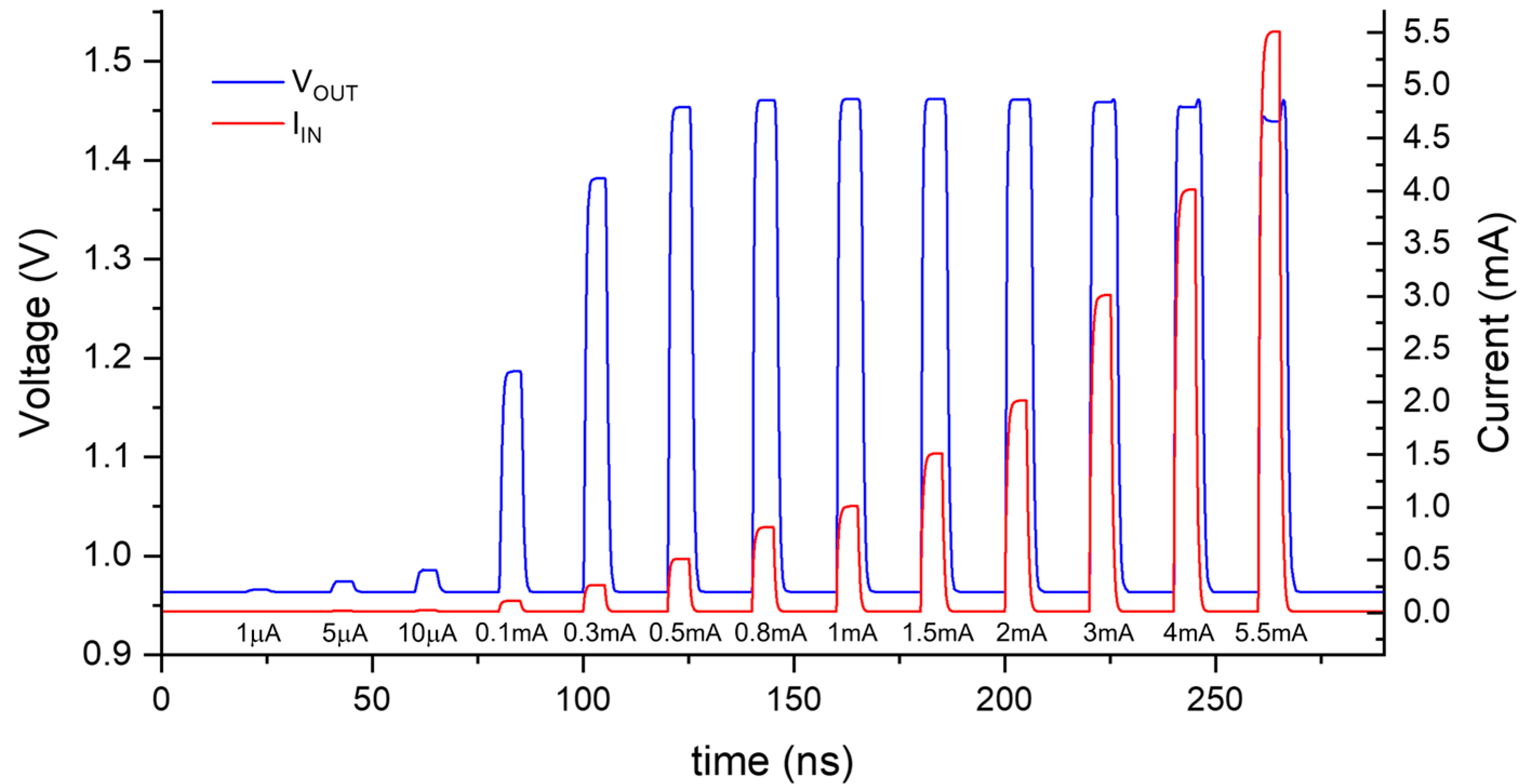
Figure 9 depicts the simulated pulse response of the OTA, in which the input currents vary within the range from 1 µApp to 5.5 mApp, and the corresponding output voltages are observed with negligible distortions. Also, it can be clearly seen that the amplitudes of the output voltages change almost linearly for input currents from 1 µApp to 200 µApp, and then the output voltages remain constant at ~500 mVpp for input currents beyond 200 µApp. Although the output voltage signals evidently exhibit distortions for input currents larger than 4 mApp, these slight distortions can be effectively eliminated by subsequently exploiting the T2V converter (shown below in Figure 10).
The above results confirm the tester abilities of the A2V and T2V converters for short-range LiDAR sensors. The A2V converter detects the difference in the amplitudes and is suitable for signals reflected from relatively longer distances that correspond to small input currents. Conversely, the T2V converter measures the time interval between the START and STOP signals and is adequate for short-range detection. In other words, particularly in the pulse simulations, the A2V converter is effective in the linear region, while the T2V converter is applicable in the region where the amplitudes can be saturated.
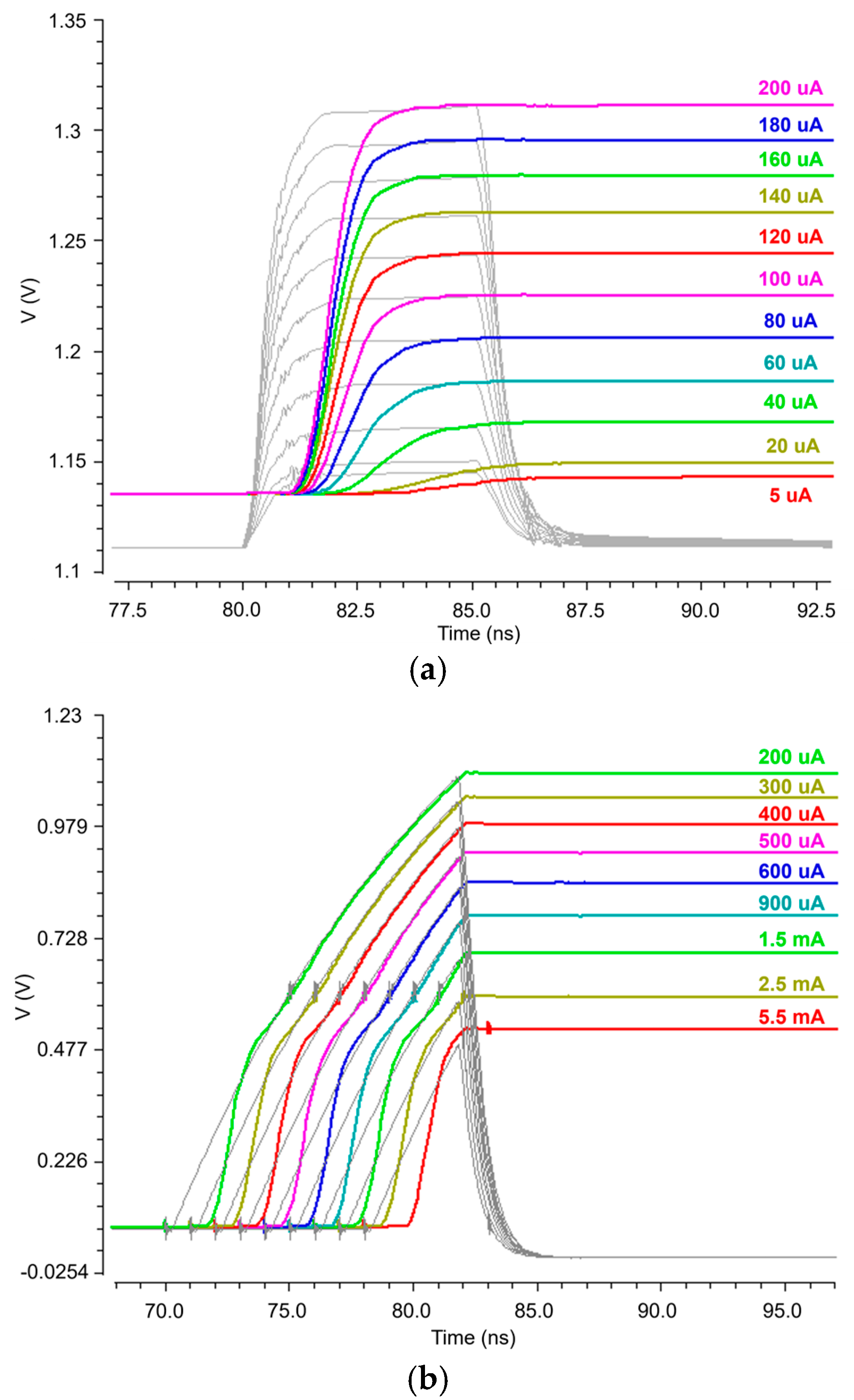
Figure 10a shows the simulated transient response of the A2V converter with variations in the input currents ranging from 5 µApp to 200 µApp, where the voltages converted by the m-TIA pass through the PA (in gray) and subsequently the PDH (represented in color). The relationship between the target distance (x) and the incoming photocurrent (iPD) is given by
x = 1 2 R × P O P T , T X i P D ,
where R is the responsivity of the on-chip APD, and P3dB is the transmitted optical power, with the assumption of 0 dBm (i.e., 1 mW). The A2V converter can be utilized to detect the distance ranging up to 10.2 m. Yet, it should also be noted here that the proposed A2V converter, as a tester circuit, cannot fully detect and recover input currents smaller than 5 µApp, which might be attributed to the slightly deficient resolution of the PDH circuit.
Figure 10b presents the simulated results of the T2V converter, where peak detection is achieved by the charging process in accordance with the time intervals between the rising edges of the START and STOP pulses. While the A2V converter can detect up to 200 µApp, the T2V converter operates effectively from 200 µApp up to a maximum current of 5.5 mApp that corresponds to the nearest detection range of 30 centimeters. Hence, a total dynamic range of 74.8 dB can be achieved by complementarily operating the A2V and T2V converters over widely various input currents.
Table 1 summarizes the performance deviations due to the process, voltage, and temperature (PVT) variations for three worst-case scenarios: (a) SS, 1.62 V and −45 °C; (b) TT, 1.8 V and 27 °C; and (c) FF, 1.98 V and 125 °C. The simulation results indicate that the proposed OTA exhibits a transimpedance (TZ) gain variation of less than 6.7%, with a bandwidth deviation of no more than 10.8% from the nominal value of 830 MHz. Also, the noise current spectral density varies by a maximum of 29%. The transient responses of the A2V converter demonstrate an output voltage swing variation of within 28% for input currents below 200 μApp. The maximum deviation of the ToF detection range is 35 centimeters. Similarly, the T2V converter output varies by 28% in case (a) for an input current of 5.5 mApp with a time-interval deviation (ΔT) of 2.4 ns. In this case, the maximum deviation of the detection range is 8.4 centimeters. Hence, these results confirm the stable operation of the proposed LiDAR receiver.
Table 2 compares the performance of the proposed LiDAR receiver with prior sensors.
Ref. [18] realized a resistive feedback TIA with a replica circuit followed by a cascaded variable-gain amplifier for the gain control mechanism. It also employed a timing discriminator with differential voltage shifters to compensate for the walk errors. However, it required a large power consumption. Ref. [19] presented a wideband receiver for a 3D ranging LiDAR system that exploited a series resistor array with PMOS switches, hence extending the dynamic range up to 64 dB. However, the control signals of the switches were generated by using multiple comparators, where an external DC voltage was required for manual gain control. Also, the proposed wideband receiver dissipated a large amount of power. Ref. [20] suggested an eight-channel receiver array that operated with two modes, i.e., either a parallel mode or a selectable mode to save power dissipation. In addition, a p-i-n photodiode was exploited for the high-gain mode while an APD was employed for the low-gain mode. However, utilizing these two photodetectors increased the implementation costs and might cause difficulties when integrating with a PC board. Moreover, the dynamic range was considerably narrower when compared to that of other works. Ref. [21] demonstrated a dual-mode AFE preamplifier which could be configured as a charge-sensitive amplifier (CSA) or as a gated active load-assisted (GALA) TIA, depending upon the intensity of the input current, thereby extending the dynamic range to 96dB. Yet, the bandwidth shrunk down to 98 MHz in CSA mode from 230 MHz in GALA-TIA. Also, the power dissipation was still large owing to the dual-mode operations. On the contrary, this work shows competent performance despite the comparatively lower responsivity of the on-chip CMOS APDs and the lower transimpedance gain characteristics. In particular, this sensor can achieve a wide dynamic range with the aid of the proposed concurrent AGC methodology, and also provide very low power dissipation and small core area characteristics.

4. Conclusions

We presented an OTA using a concurrent AGC mechanism realized using a 180 nm CMOS technology, comprising a main transimpedance amplifier with an on-chip P+/NW/DNW APD and a replica TIA with another on-chip APD to render the concurrent AGC function feasible within a narrow single pulse width. The post-layout simulations revealed that the OTA can extend the dynamic range up to 74.8 dB (i.e., 1 µApp~5.5 mApp) and achieve a 67 dBΩ transimpedance gain, an 830 MHz bandwidth, a −31 dBm optical sensitivity for a 10−12 BER with the assumption of 4.61 A/W APD responsivity, and a 6 mW power dissipation. Conclusively, the proposed OTA can be a highly efficient solution for application to low-power, low-cost, short-range LiDAR sensors.

Author Contributions

Conceptualization, S.-M.P.; methodology, S.-M.P.; validation, Y.C. and S.C.; writing—original draft preparation, Y.C., S.C. and S.-M.P.; writing—review and editing, Y.C., S.C. and S.-M.P.; visualization, Y.C. and S.C.; supervision, S.-M.P.; project administration, S.-M.P.; funding acquisition, S.-M.P. All authors have read and agreed to the published version of the manuscript.

Funding

This research was supported by the MSIT (Ministry of Science and ICT), Republic of Korea, under the ITRC (Information Technology Research Center) support program (IITP-2020-0-01847), supervised by the IITP (Institute for Information & Communications Technology Planning & Evaluation). In addition, this work was supported by the National Research Foundation (NRF), Republic of Korea, under project BK21 FOUR.

Institutional Review Board Statement

Not applicable.

Informed Consent Statement

Not applicable.

Data Availability Statement

Data are contained within the article.

Acknowledgments

The EDA tool was supported by the IC Design Education Center (IDEC), Republic of Korea.

Conflicts of Interest

The authors declare no conflicts of interest.

References

  1. Raj, T.; Hanim Hashim, F.; Baseri Huddin, A.; Ibrahim, M.F.; Hussain, A. A Survey on LiDAR Scanning Mechanisms. Electronics 2020, 9, 741. [Google Scholar] [CrossRef]
  2. Frøvik, N.; Malekzai, B.A.; Øvsthus, K. Utilising LiDAR for fall detection. Healthc. Technol. Lett. 2021, 8, 11–17. [Google Scholar] [CrossRef] [PubMed]
  3. Wang, Y.-T.; Peng, C.-C.; Ravankar, A.A.; Ravankar, A. A Single LiDAR-Based Feature Fusion Indoor Localization Algorithm. Sensors 2018, 18, 1294. [Google Scholar] [CrossRef] [PubMed]
  4. Fraccaro, P.; Evangelopoulos, X.; Edwards, B. Development and Preliminary Evaluation of a Method for Passive, Privacy-Aware Home Care Monitoring Based on 2D LiDAR Data. Artif. Intell. Med. 2020, 12299, 160–169. [Google Scholar]
  5. Taramasco, C.; Rodenas, T.; Martinez, F.; Fuentes, P.; Munoz, R.; Olivares, R.; De Albuquerque, V.H.C.; Demongeot, J. A novel monitoring system for fall detection in older people. IEEE Access 2018, 6, 43563–43574. [Google Scholar] [CrossRef]
  6. Hong, C.; Kim, S.-H.; Kim, J.-H.; Park, S.M. A Linear-Mode LiDAR Sensor Using a Multi-Channel CMOS Transimpedance Amplifier Array. IEEE Sens. J. 2018, 18, 7032–7040. [Google Scholar] [CrossRef]
  7. Yan, C.; Mao, L.; Zhang, S.; Xie, S.; Xiao, X.; Tian, Y.; Yang, C. An optical receiver with automatic gain control for radio-over-fiber system. In Proceedings of the 2011 IEEE International Conference of Electron Devices and Solid-State Circuits (EDDSC), Tianjin, China, 17–18 November 2011. [Google Scholar]
  8. Dziallas, G.; Fatemi, A.; Malignaggi, A.; Kahmen, G. A Monolithic-Integrated Broadband Low-Noise Optical Receiver with Automatic Gain Control in 0.25μm SiGe BiCMOS. In Proceedings of the IEEE 20th Topical Meeting on Silicon Monolithic ICs in RF Systems (SiRF), San Diego, CA, USA, 17–20 January 2021. [Google Scholar]
  9. Khafaji, M.M.; Belfiore, G.; Ellinger, F. A Linear 65-GHz Bandwidth and 71-dBΩ Gain TIA with 7.2 pA/√Hz in 130-nm SiGe BiCMOS. IEEE Solid-State Circuits Lett. 2021, 4, 76–79. [Google Scholar] [CrossRef]
  10. Wang, J.; Pan, Q.; Qin, Y.; Chen, X.; Hu, S.; Bai, R.; Wang, X.; Cai, Y.; Xia, T.; Zhang, Y.; et al. A Fully Integrated 25 Gb/s Low-Noise TIA+CDR Optical Receiver Designed in 40-nm-CMOS. IEEE Trans. Circuits Syst. II Express Briefs 2019, 66, 1698–1702. [Google Scholar] [CrossRef]
  11. Yoon, D.; Joo, J.-E.; Park, S.M. Mirrored Current-Conveyor Transimpedance Amplifier for Home Monitoring LiDAR Sensors. IEEE Sens. J. 2021, 21, 5589–5597. [Google Scholar] [CrossRef]
  12. Razavi, B. Design of Integrated Circuits for Optical Communications; Wiley: Hoboken, NJ, USA, 2012. [Google Scholar]
  13. Lee, M.-J.; Choi, W.-Y. Performance comparison of two types of silicon avalanche photodetectors based on N-well/P-substrate and P+/N-well junctions fabricated with standard CMOS technology. J. Opt. Soc. Korea 2011, 15, 1–3. [Google Scholar] [CrossRef]
  14. Nguyen, V.N.; Duong, D.N.; Chung, Y.; Lee, J.W. A Cyclic Vernier Two-Step TDC for High Input Range Time-of-Flight Sensor Using Startup Time Correction Technique. Sensors 2018, 18, 3948. [Google Scholar] [CrossRef] [PubMed]
  15. He, Y.; Park, S.M. A CMOS Integrator-Based Clock-Free Time-to-Digital Converter for Home-Monitoring LiDAR Sensors. Sensors 2022, 22, 554. [Google Scholar] [CrossRef] [PubMed]
  16. Liu, M.; Liu, H.; Li, X.; Zhu, Z. A 60-m range 6.16-mW laser-power linear-mode LiDAR system with multiplex ADC/TDC in 65-nm CMOS. IEEE Trans. Circuits Syst. I Regul. Pap. 2019, 67, 753–764. [Google Scholar] [CrossRef]
  17. Hu, Y.; Joo, J.-E.; Zhang, X.; Chon, Y.; Choi, S.; Lee, M.-J.; Park, S.-M. A Current-Mode Optoelectronic Receiver IC for Short-Range LiDAR Sensors in 180 nm CMOS. Photonics 2023, 10, 746. [Google Scholar] [CrossRef]
  18. Zheng, H.; Ma, R.; Liu, M.; Zhu, Z. A Linear Dynamic Range Receiver with Timing Discrimination for Pulsed TOF Imaging LADAR Application. IEEE Trans. Instrum. Meas. 2018, 67, 2684–2691. [Google Scholar] [CrossRef]
  19. Li, K.; Guo, J.; Zhao, Y. A CMOS AFE With 37-nArms Input-Referred Noise and Marked 96-dB Timing DR for Pulsed LiDAR. IEEE Trans. Circuits Syst. I Regul. Pap. 2022, 69, 3565–3578. [Google Scholar] [CrossRef]
  20. Yang, Y.; Liu, X.; Yang, R.; Ma, S.; Xia, Y.; Li, J.; Zhang, B.; Geng, L.; Li, D. A Low-Power Multimode Eight-Channel AFE for dToF LiDAR. In Proceedings of the 2024 IEEE International Symposium on Circuits and Systems (ISCAS), Singapore, 19–22 May 2024. [Google Scholar]
  21. Ngo, T.-H.; Kim, C.-H.; Kwon, Y.J.; Ko, J.S.; Kim, D.-B.; Park, H.-H. Wideband Receiver for a Three-Dimensional Ranging LADAR System. IEEE Trans. Circuits Syst. I Regul. Pap. 2013, 60, 448–456. [Google Scholar] [CrossRef]
  22. Joo, J.-E.; Hu, Y.; Kim, S.; Kim, H.; Park, S.; Kim, J.-H.; Kim, Y.; Park, S.-M. An Indoor-Monitoring LiDAR Sensor for Patients with Alzheimer Disease Residing in Long-Term Care Facilities. Sensors 2022, 22, 7934. [Google Scholar] [CrossRef] [PubMed]
Figure 1. Block diagram of (a) a traditional optical receiver with AGC and (b) a previously reported MCC-TIA with a single-pulse AGC [11].
Photonics 11 00974 g001
Figure 2. Block diagram of proposed optoelectronic transimpedance amplifier (OTA).
Photonics 11 00974 g002
Figure 3. Schematic diagrams of (a) the m-TIA and (b) the replica TIA.
Photonics 11 00974 g003
Figure 4. (a) Cross-sectional view of P+/NW/DNW APD and (b) its layout and measured results.
Photonics 11 00974 g004
Figure 5. (a) A block diagram of the test circuitry for the proposed OTA and (b) a schematic diagram of the utilized PDH circuit.
Photonics 11 00974 g005
Figure 6. (a) A block diagram of T2V converter and (b) a schematic diagram of latch comparator.
Photonics 11 00974 g006
Figure 7. Layout of proposed LiDAR receiver.
Photonics 11 00974 g007
Figure 8. (a) The simulated frequency response of the proposed OTA and (b) the gain variation with the proposed concurrent AGC.
Photonics 11 00974 g008
Figure 9. Simulated pulse response of the proposed OTA for the different input currents.
Photonics 11 00974 g009
Figure 10. Simulated pulse responses of (a) the A2V converter with different input currents and (b) the T2V converter for various time intervals.
Photonics 11 00974 g010
Table 1. PVT variation simulations of the proposed LiDAR receiver.
ParametersSS
1.62 V, −45 °C
TT
1.8 V, 27 °C
FF
1.98 V, 125 °C
OTATZ gain (dBΩ)69 (+3.1%)66.962.4 (−6.7%)
Bandwidth (MHz)740 (−10.8%)830758 (−8.67%)
Noise current spectral density (pA/ Hz )12.4 (−21.5%)15.820.4 (+29%)
A2VOutput voltage amplitude (Vpp)
@ 5 µApp input current
0.94 (−17%)1.131.35 (+19%)
Output voltage amplitude (Vpp)
@ 200 µApp input current
1.25 (+11%)1.121.44 (+28%)
T2VOutput voltage amplitude (Vpp)
@ 200 µApp (Δt = 10.7 ns) input current
0.92 (−14%)1.071.16 (+8.4%)
Output voltage amplitude (Vpp)
@ 5.5 mApp (Δt = 2.4 ns) input current
0.36 (−28%)0.5050.54 (+6.9%)
Table 2. Performance comparison with previously reported LiDAR sensors.
Parameters[18][19][20][21][22]This Work
CMOS technology (nm)180130180180180180
APDTypeOff chipOff chipOff chipOff chipOn chipOn chip
Cpd (pF)1231.20.50.5
Responsivity (A/W)3232N/A502.724.16
Wavelength (nm)N/AN/AN/A905850850
Max. TZ gain (dBΩ)106781008795.167
Gain controlYesYesYesYesNoYes
Bandwidth (MHz)150640180230608830
Min. detectable current (µApp)0.55.65.00.63.41.0
Max. detectable current (mApp)1.09.02.05.0N/A5.5
LinearityLinearLinearN/ALinearN/ALinear ξ
Dynamic range (dB)66645296N/A74.8
Power dissipation per channel (mW)165 *11449.3/10.56620.96
Chip area (mm2)0.9 (1ch †)0.6 (1ch †)5 (8ch †)0.33(1ch †)0.23 (1ch †)0.95 (Rx 2ch †)
0.24 (core)
† ch = channel; * 3.3 V VDD; ξ with A2V converter handling up to 200 µApp.
Disclaimer/Publisher’s Note: The statements, opinions and data contained in all publications are solely those of the individual author(s) and contributor(s) and not of MDPI and/or the editor(s). MDPI and/or the editor(s) disclaim responsibility for any injury to people or property resulting from any ideas, methods, instructions or products referred to in the content.